Front Matter
Arm® Generic Interrupt Controller Architecture Specification GIC architecture version 3 and version 4

Copyright © 2008, 2011, 2015-2021 Arm Limited or its affiliates. All rights reserved.
Arm Generic Interrupt Controller Architecture Specification GIC architecture version 3 and version 4
Copyright © 2008, 2011, 2015-2021 Arm Limited or its affiliates. All rights reserved.
Release Information
The following changes have been made to this document.

Change History
| Date | Issue | Confidentiality | Change |
|---|---|---|---|
| June 2015 | A | Non-confidential | First release of GICv3 and GICv4 issue A. |
| December 2015 | B | Non-confidential | First release of GICv3 and GICv4 issue B. |
| July 2016 | C | Non-confidential | First release of GICv3 and GICv4 issue C. |
| August 2017 | D | Non-confidential | First release of GICv3 and GICv4 issue D. |
| January 2019 | E | Non-confidential | First release of GICv3 and GICv4 issue E. |
| February 2020 | F | Non-confidential | First release of GICv3 and GICv4.1 issue F. |
| February 2021 | G | Non-confidential | First release of GICv3 and GICv4.1 issue G. |
Some of the information in this specification was previously published in Arm[®] Generic Interrupt Controller, Architecture version 2.0, Architecture Specification .
Proprietary Notice
This document is protected by copyright and other related rights and the practice or implementation of the information contained in this document may be protected by one or more patents or pending patent applications. No part of this document may be reproduced in any form by any means without the express prior written permission of ARM. No license, express or implied, by estoppel or otherwise to any intellectual property rights is granted by this document unless specifically stated.
Your access to the information in this document is conditional upon your acceptance that you will not use or permit others to use the information for the purposes of determining whether implementations infringe any third party patents.
THIS DOCUMENT IS PROVIDED “AS IS”. ARM PROVIDES NO REPRESENTATIONS AND NO WARRANTIES, EXPRESS, IMPLIED OR STATUTORY, INCLUDING, WITHOUT LIMITATION, THE IMPLIED WARRANTIES OF MERCHANTABILITY, SATISFACTORY QUALITY, NON-INFRINGEMENT OR FITNESS FOR A PARTICULAR PURPOSE WITH RESPECT TO THE DOCUMENT. For the avoidance of doubt, ARM makes no representation with respect to, and has undertaken no analysis to identify or understand the scope and content of, patents, copyrights, trade secrets, or other rights.
This document may include technical inaccuracies or typographical errors.
TO THE EXTENT NOT PROHIBITED BY LAW, IN NO EVENT WILL ARM BE LIABLE FOR ANY DAMAGES, INCLUDING WITHOUT LIMITATION ANY DIRECT, INDIRECT, SPECIAL, INCIDENTAL, PUNITIVE, OR CONSEQUENTIAL DAMAGES, HOWEVER CAUSED AND REGARDLESS OF THE THEORY OF LIABILITY, ARISING OUT OF ANY USE OF THIS DOCUMENT, EVEN IF ARM HAS BEEN ADVISED OF THE POSSIBILITY OF SUCH DAMAGES.
This document consists solely of commercial items. You shall be responsible for ensuring that any use, duplication or disclosure of this document complies fully with any relevant export laws and regulations to assure that this document or any portion thereof is not exported, directly or indirectly, in violation of such export laws. Use of the word “partner” in reference to ARM’s customers is not intended to create or refer to any partnership relationship with any other company. ARM may make changes to this document at any time and without notice.
If any of the provisions contained in these terms conflict with any of the provisions of any click through or signed written agreement covering this document with ARM, then the click through or signed written agreement prevails over and supersedes the conflicting provisions of these terms. This document may be translated into other languages for convenience, and you agree that if there is any conflict between the English version of this document and any translation, the terms of the English version of the Agreement shall prevail.
The ARM corporate logo and words marked with ® or ™ are registered trademarks or trademarks of ARM Limited (or its subsidiaries) in the US and/or elsewhere. All rights reserved. Other brands and names mentioned in this document may be the trademarks of their respective owners. Please follow ARM’s trademark usage guidelines at http://www.arm.com/company/policies/trademarks. Copyright © 2008, 2011, 2015-2021 Arm Limited or its affiliates. All rights reserved.
Arm Limited. Company 02557590 registered in England.
110 Fulbourn Road, Cambridge, England CB1 9NJ.
LES-PRE-20349
Confidentiality Status
This document is Non-Confidential. The right to use, copy and disclose this document may be subject to license restrictions in accordance with the terms of the agreement entered into by Arm and the party that Arm delivered this document to.
Product Status
The information in this document is final, that is for a developed product.
Web Address
http://www.arm.com
Progressive terminology commitment
Arm values inclusive communities. Arm recognizes that we and our industry have used terms that can be offensive. Arm strives to lead the industry and create change.
Previous issues of this document included terms that can be offensive. We have replaced these terms.
If you find offensive terms in this document, please contact [email protected].
Contents Arm Generic Interrupt Controller Architecture Specification GIC architecture version 3 and version 4
| Preface | |||
|---|---|---|---|
| About this specification | |||
| Using this specification | |||
| Conventions | |||
| Additional reading | |||
| Feedback | |||
| Chapter | 1 | Introduction | |
| — | — | — | — |
| 1.1 | About the Generic Interrupt Controller (GIC) | ||
| 1.2 | Terminology | ||
| 1.3 | Supported configurations and compatibility | ||
| Chapter | 2 | Distribution and Routing of Interrupts | |
| 2.1 | The Distributor and Redistributors | ||
| 2.2 | INTIDs | ||
| 2.3 | Affinity routing | ||
| Chapter | 3 | GIC Partitioning | |
| 3.1 | The GIC logical components | ||
| 3.2 | Interrupt bypass support | ||
| Chapter | 4 | Physical Interrupt Handling and Prioritization | |
| 4.1 | Interrupt lifecycle | ||
| 4.2 | Locality-specific Peripheral Interrupts | ||
| 4.3 | Private Peripheral Interrupts | ||
| 4.4 | Software Generated Interrupts | ||
| 4.5 | Shared Peripheral Interrupts | ||
| 4.6 | Interrupt grouping | ||
| 4.7 | Enabling the distribution of interrupts | ||
| 4.8 | Interrupt prioritization | ||
| Chapter | 5 | Locality-specific Peripheral Interrupts and the ITS | |
| 5.1 | LPIs | ||
| 5.2 | The Interrupt Translation Service | ||
| 5.3 | ITS commands | ||
| 5.4 | Common ITS pseudocode functions | ||
| 5.5 | ITS command error encodings | ||
| 5.6 | ITS power management | ||
| Chapter | 6 | Virtual Interrupt Handling and Prioritization | |
| 6.1 | About GIC support for virtualization | ||
| 6.2 | Operation overview | ||
| 6.3 | Configuration and control of VMs | ||
| 6.4 | Pseudocode | ||
| Chapter | 7 | GICv4.0 Virtual LPI Support | |
| 7.1 | About GICv4.0 virtual Locality-specific Peripheral Interrupt support | ||
| 7.2 | Direct injection of virtual interrupts | ||
| Chapter | 8 | GICv4.1 Virtual Interrupt Support | |
| 8.1 | About GICv4.1 virtual interrupt support | ||
| 8.2 | Changes to the CPU interface | ||
| 8.3 | ITS commands | ||
| 8.4 | vPEID width | ||
| 8.5 | Doorbells | ||
| 8.6 | vPE residency and locating data structures | ||
| 8.7 | Register based vLPI invalidation | ||
| 8.8 | Direct injection of vSGIs | ||
| Chapter | 9 | Memory Partitioning and Monitoring | |
| 9.1 | Overview | ||
| 9.2 | MPAM and the Redistributors | ||
| 9.3 | MPAM and the ITS | ||
| 9.4 | GIC usage of MPAM | ||
| 9.5 | GICv4.1 data structures and MPAM | ||
| Chapter | 10 | Connecting to Armv8-R AArch64 PEs | |
| 10.1 | Armv8-R AArch64 CPU interface requirements | ||
| Chapter | 11 | Power Management | |
| 11.1 | Power management | ||
| Chapter | 12 | Programmers’ Model | |
| 12.1 | About the programmers’ model | ||
| 12.2 | AArch64 System register descriptions | ||
| 12.3 | AArch64 System register descriptions of the virtual registers | ||
| 12.4 | AArch64 virtualization control System registers | ||
| 12.5 | AArch32 System register descriptions | ||
| 12.6 | AArch32 System register descriptions of the virtual registers | ||
| 12.7 | AArch32 virtualization control System registers | ||
| 12.8 | The GIC Distributor register map | ||
| 12.9 | The GIC Distributor register descriptions | ||
| 12.10 | The GIC Redistributor register map | ||
| 12.11 | The GIC Redistributor register descriptions | ||
| 12.12 | The GIC CPU interface register map | ||
| 12.13 | The GIC CPU interface register descriptions | ||
| 12.14 | The GIC virtual CPU interface register map | ||
| 12.15 | The GIC virtual CPU interface register descriptions | ||
| 12.16 | The GIC virtual interface control register map | ||
| 12.17 | The GIC virtual interface control register descriptions | ||
| 12.18 | The ITS register map | ||
| 12.19 | The ITS register descriptions | ||
| 12.20 | Pseudocode | ||
| Chapter | 13 | System Error Reporting | |
| 13.1 | About System Error reporting | ||
| Chapter | 14 | Legacy Operation and Asymmetric Configurations | |
| 14.1 | Legacy support of interrupts and asymmetric configurations | ||
| 14.2 | The asymmetric configuration | ||
| 14.3 | Support for legacy operation of VMs | ||
| Appendix A | GIC Stream Protocol interface | ||
| A.1 | Overview | ||
| A.2 | Signals and the GIC Stream Protocol | ||
| A.3 | The GIC Stream Protocol | ||
| A.4 | Alphabetic list of command and response packet formats | ||
| Appendix B | Pseudocode Definition | ||
| B.1 | About Arm pseudocode | ||
| B.2 | Data types | ||
| B.3 | Expressions | ||
| B.4 | Operators and built-in functions | ||
| B.5 | Statements and program structure | ||
| B.6 | Pseudocode terminology | ||
| B.7 | Miscellaneous helper procedures and support functions |
Glossary
vii viii
Preface
This preface introduces the Arm[®] Generic Interrupt Controller Architecture Specification . It contains the following sections:
-
About this specification on page x.
-
Using this specification on page xi.
-
Conventions on page xiii.
-
Additional reading on page xiv.
-
Feedback on page xv. Preface About this specification
About this specification
This specification describes the Arm Generic Interrupt Controller (GIC) architecture. It defines versions 3.0, 3.1, 3.2 (GICv3), 4.0, and 4.1 (GICv4) of the GIC architecture.
Throughout this document, references to the GIC or a GIC refer to a device that implements the GIC architecture. Unless the context makes it clear that a reference is to an IMPLEMENTATION DEFINED feature of the device, these references describe the requirements of this specification.
Intended audience
This specification is for users who want to design, implement, or program the GIC in a range of Arm-compliant implementations, from simple uniprocessor implementations to complex multiprocessor systems. It does not assume familiarity with previous versions of the GIC.
The specification assumes that users have some experience of Arm products, and are familiar with the terminology that describes the Armv8 architecture. See the Arm[®] Architecture Reference Manual, Armv8, for Armv8-A architecture profile for more information. Preface Using this specification
Using this specification
This specification is organized into the following chapters:
Chapter 1 Introduction
Read this for an overview of the GIC, and information about the terminology that this document uses.
Chapter 2 Distribution and Routing of Interrupts
Read this for information about how the GIC uses affinity routing to distribute interrupts.
Chapter 3 GIC Partitioning
Read this for an overview of the GIC partitioning and information about the GIC logical components. Chapter 4 Physical Interrupt Handling and Prioritization Read this for information about how the GIC handles physical interrupts. Chapter 5 Locality-specific Peripheral Interrupts and the ITS Read this for a description of Locality-specific Peripheral Interrupts (LPIs) and the use of the Interrupt Translation Service (ITS). Chapter 6 Virtual Interrupt Handling and Prioritization Read this for information about how the GIC handles virtual interrupts. Chapter 7 GICv4.0 Virtual LPI Support
Read this for information about how the GIC handles virtual interrupts. Chapter 8 GICv4.1 Virtual Interrupt Support Read this for information about changes to virtual interrupt support in GICv4.1. Chapter 9 Memory Partitioning and Monitoring Read this for a description of Memory Partitioning and Monitoring in the context of the GIC. Chapter 10 Connecting to Armv8-R AArch64 PEs Read this for information about connecting a GIC to PEs that implement Armv8-R64. Chapter 11 Power Management Read this for information about GIC power management. Chapter 12 Programmers’ Model Read this for a description of the GIC register interfaces, and all GIC registers. Chapter 13 System Error Reporting Read this for information about GIC support for error reporting. Chapter 14 Legacy Operation and Asymmetric Configurations Read this for information about GIC support for legacy operation and asymmetric configurations. Appendix A GIC Stream Protocol interface
Read this for a description of the AXI4-Stream protocol standard message-based interface that the GIC Stream Protocol interface uses.
Appendix B Pseudocode Definition
Read this for a definition of the pseudocode that is used in this specification.
Glossary
Read this for definitions of some of the terms used in this specification. Preface Using this specification
Preface Conventions
Conventions
The following sections describe conventions that this book can use:
-
Typographic conventions .
-
Signals .
-
Numbers .
-
Pseudocode descriptions .
Typographic conventions
The typographical conventions are:
italic Introduces special terminology, and denotes citations. bold Denotes signal names, and is used for terms in descriptive lists, where appropriate. monospace Used for assembler syntax descriptions, pseudocode, and source code examples. Also used in the main text for instruction mnemonics and for references to other items appearing in assembler syntax descriptions, pseudocode, and source code examples.
SMALL CAPITALS
Used for a few terms that have specific technical meanings, and are included in the Glossary .
Colored text Indicates a link. This can be:
-
A URL, for example https://developer.arm.com.
-
A cross-reference, that includes the page number of the referenced information if it is not on the current page, for example, About the Generic Interrupt Controller (GIC) on page 1-18.
-
A link, to a chapter or appendix, or to a glossary entry, or to the section of the document that defines the colored term, for example, Banked register or GICC_CTLR.
Signals
In general this specification does not define processor signals, but it does include some signal examples and recommendations. The signal conventions are:
Signal level The level of an asserted signal depends on whether the signal is active-HIGH or active-LOW. Asserted means:
-
HIGH for active-HIGH signals
-
LOW for active-LOW signals.
Lowercase n At the start or end of a signal name denotes an active-LOW signal.
Numbers
Numbers are normally written in decimal. Binary numbers are preceded by 0b, and hexadecimal numbers by 0x. In both cases, the prefix and the associated value are written in a monospace font, for example 0xFFFF0000.
Pseudocode descriptions
This specification uses a form of pseudocode to provide precise descriptions of the specified functionality. This pseudocode is written in a monospace font, and follows the conventions described in the Arm[®] Architecture Reference Manual, Armv8, for Armv8-A architecture profile and the Arm[®] Architecture Reference Manual, Armv7-A and Armv7-R edition . Preface Additional reading
Additional reading
This section lists relevant publications from Arm and third parties.
See Arm Developer, https://developer.arm.com for access to Arm documentation.
Arm publications
-
AMBA[®] 4 AXI4-Stream Protocol Specification (ARM IHI 0051).
-
Arm[®] Architecture Reference Manual, Armv7-A and Armv7-R edition (ARM DDI 0406).
-
Arm[®] Architecture Reference Manual, Armv8, for Armv8-A architecture profile (ARM DDI 0487).
-
Arm[®] Architecture Reference Manual Supplement, Memory System Resource Partitioning and Monitoring (MPAM), for Armv8-A (ARM DDI 0598).
-
Arm[®] Generic Interrupt Controller, Architecture version 2.0, Architecture Specification (ARM IHI 0048).
-
Arm[®] CoreSight[™] Architecture Specification v3.0 (ARM IHI 0029).
-
Arm[®] Server Base System Architecture (SBSA) (ARM-DEN-0029).
-
GICv3 and GICv4 Software Overview (DAI 0492).
-
• Application Note GIC Stream Protocol Interface (ARM-ECM-0495013).
Other publications
The following books are referred to in this manual, or provide more information:
- JEDEC Solid State Technology Association, Standard Manufacture’s Identification Code , JEP106. Preface Feedback
Feedback
Arm welcomes feedback on its documentation.
Feedback on this manual
-
If you have comments on the content of this manual, send an e-mail to [email protected]. Provide: • The title.
-
The number, Arm IHI 0069G.
-
The page numbers to which your comments apply.
-
A concise explanation of your comments.
Arm also welcomes general suggestions for additions and improvements. Preface Feedback
Chapter 1: Introduction
This chapter provides an introduction to the GIC architecture. It provides an overview of the GIC architecture, and the features that are new to the architecture. It also provides definitions of the terminology that this document uses. It contains the following sections:
-
About the Generic Interrupt Controller (GIC) .
-
Terminology .
-
Supported configurations and compatibility . 1.1 About the Generic Interrupt Controller (GIC)
1.1 About the Generic Interrupt Controller (GIC)
The GICv3 architecture is designed to operate with Armv8-A and Armv8-R compliant processing elements , PEs.
The Generic Interrupt Controller (GIC) architecture defines:
-
The architectural requirements for handling all interrupt sources for any PE connected to a GIC.
-
A common interrupt controller programming interface applicable to uniprocessor or multiprocessor systems.
The GIC is an architected resource that supports and controls interrupts. It provides:
-
Registers for managing interrupt sources, interrupt behavior, and the routing of interrupts to one or more PEs.
-
Support for:
- The Armv8 architecture.
-
Locality-specific Peripheral Interrupts (LPIs).
- Private Peripheral Interrupts (PPIs).
-
Software Generated Interrupts (SGIs).
-
Shared Peripheral Interrupts (SPIs).
-
Interrupt masking and prioritization.
-
Uniprocessor and multiprocessor systems.
-
-
Wakeup events in power management environments.
For each PE, the GIC architecture describes how IRQ and FIQ interrupts can be generated from different types of interrupts within the system. The Armv8-A Exception model describes how the PE handles these IRQ and FIQ interrupts.
Interrupt handling also depends on other aspects of the Armv8 architecture, such as the Security state and support for virtualization. The Arm architecture provides two Security states, each with an associated physical memory address space:
-
Secure state.
-
Non-secure state.
The GIC architecture supports the routing and handling of interrupts that are associated with both Security states. See Interrupt grouping and security for more information.
The GIC architecture supports the Armv8 model for handling virtual interrupts that are associated with a virtual machine , VM. A virtualized system has:
-
A hypervisor that must include a component executing at EL2, that is responsible for switching between VMs.
-
Several VMs executing at EL1.
-
Applications executing at EL0 on a VM.
For more information about the Armv8 architecture, see Arm[®] Architecture Reference Manual, Armv8, for Armv8-A architecture profile . For more information about VMs, see About GIC support for virtualization .
This specification defines version 3.0, version 3.1, version 3.2 (collectively GICv3), version 4.0, and version 4.1 (collectively GICv4.1) of the GIC architecture. Version 2.0 (GICv2) is only described in terms of the GICv3 optional support for legacy operation, see GICv3 with legacy operation . For detailed information about the GICv2 architecture, see the Arm[®] Generic Interrupt Controller, Architecture version 2.0, Architecture Specification .
Note Because GICv4 is an extension of GICv3.0 and GICv3.1, all references to GICv3 in this manual apply equally to GICv4, unless explicitly indicated otherwise. Any changes to the architecture specification for GICv4.1 are indicated accordingly.
1.1.1 Changes to the GIC architecture from GICv2
GIC scalability
The GICv2 architecture only supports a maximum of eight PEs, and so has features that do not scale to a large system. GICv3 addresses this by changing the mechanism by which interrupts are routed, called affinity routing , and by introducing a new component to the interrupt distribution, called a Redistributor . See Chapter 3 GIC Partitioning for more information.
Affinity routing for a Security state is enabled by setting GICD_CTLR.ARE_S or GICD_CTLR.ARE_NS to 1.
Interrupt grouping
Interrupt grouping is the mechanism that is used by GICv3 to align interrupt handling with the Armv8 Exception model:
-
Group 0 physical interrupts are expected to be handled at the highest implemented Exception level.
-
Secure Group 1 physical interrupts are expected to be handled at Secure EL1 or EL2.
-
Non-secure Group 1 physical interrupts are excepted to be handled at Non-secure EL2 in systems using virtualization, or at Non-secure EL1 in systems not using virtualization.
These interrupt groups can be mapped onto the Armv8 FIQ and IRQ signals as described in Interrupt grouping , using configuration bits from the Armv8 architecture and the configuration bits within the GICv3 architecture.
In GICv3, interrupt grouping supports:
-
Configuring each interrupt as Group 0, Secure Group 1, or Non-secure Group 1.
-
Signaling Group 0 physical interrupts to the target PE using the FIQ exception request.
-
Signaling Group 1 physical interrupts to the target PE in a manner that allows them to be handled using the IRQ handler in their own Security state. The exact handling of Group 1 interrupts depends on the current Exception level and Security state, as described in Chapter 4 Physical Interrupt Handling and Prioritization .
-
A unified scheme for handling the priority of Group 0 and Group 1 interrupts.
Interrupt Translation Service (ITS)
The Interrupt Translation Service, ITS, provides functionality that allows software to control how interrupts that are forwarded to the ITS are translated into:
-
Physical interrupts, in GICv3 and GICv4.
-
Virtual interrupts, in GICv4 only.
The ITS also allows software to determine the target Redistributor for a translated interrupt. Software can control the ITS through a command interface and associated table-based structures in memory. The outputs of the Interrupt Translation Service (ITS) are always LPIs, which are a form of message-based interrupt. See The Interrupt Translation Service .
Locality-specific Peripheral Interrupts (LPIs)
LPIs are a new class of interrupt that significantly extends the interrupt ID space that the GIC can handle. LPIs are optional, and, if implemented, can be generated and supported by an Interrupt Translation Service, ITS. See LPIs .
Software Generated Interrupts (SGIs)
With the ability of GICv3 to support large-scale systems, the context of an SGI is modified and no longer includes the identity of the source PE. See Software Generated Interrupts .
Note
The original SGI format is only available in GIC implementations that support legacy operation.
Shared Peripheral Interrupts (SPIs)
A new set of registers in the Distributor is added to support the setting and clearing of message-based SPIs. See Shared Peripheral Interrupts .
System register interface
This interface uses System register instructions in an Armv8-A or Armv8-R PE to provide a closely-coupled interface for the CPU interface registers. This interface is used for registers that are associated directly with interrupt handling and priority masking to minimize access latency. For virtualization, the registers that are accessed in this manner include both the registers that are accessed by a VM interrupt handler, and the registers that forward virtual interrupts from a hypervisor to a VM. All other registers are memory-mapped.
For AArch64 state, access to the System register interface is enabled by the following settings:
-
ICC_SRE_EL1.SRE == 1.
-
• ICC_SRE_EL2.SRE == 1. • ICC_SRE_EL3.SRE == 1.
For AArch32 state, access to the System register interface is enabled by the following settings: • ICC_SRE.SRE == 1. • ICC_HSRE.SRE == 1. • ICC_MSRE.SRE == 1.
Other behavior, which is backwards compatible with GICv2, is described in Chapter 14 Legacy Operation and Asymmetric Configurations .
Note
In a GIC that supports legacy operation, memory-mapped access is available for all architected GIC registers.
Unless indicated otherwise, this manual describes the GICv3 architecture in a system with affinity routing, System register access, and two Security states, enabled. This means that:
-
GICD_CTLR.ARE_NS == 1.
-
• GICD_CTLR.ARE_S == 1. • GICD_CTLR.DS == 0.
For operation in AArch64 state:
-
ICC_SRE_EL1.SRE == 1, for both the Secure and the Non-secure copy of this register.
-
ICC_SRE_EL2.SRE == 1.
-
ICC_SRE_EL3.SRE == 1.
For operation in AArch32 state:
-
ICC_SRE.SRE == 1.
-
ICC_HSRE.SRE == 1.
-
ICC_MSRE.SRE == 1.
From GICv3 onwards, legacy operation with the ARE and SRE control bits set to 0 is deprecated, and removed if the PE implements Secure EL2. See Chapter 14 Legacy Operation and Asymmetric Configurations for more information about legacy operation.
Changes specific to GICv3.1
GICv3.1 adds support for Memory Partitioning and Monitoring, an extended SPI range, an extended PPI range, and support for Secure EL2.
Changes specific to GICv3.2
GICv3.2 adds support for Armv8-R AArch64.
Changes specific to GICv4
GICv4 adds support for the direct injection of virtual interrupts to a VM, without involving the hypervisor. Direct injections are only supported by systems that implement at least one ITS that translates interrupts into LPIs.
Changes specific to GICv4.1
GICv4.1 extends direct injection support to also handle virtual SGIs. GICv4.1 changes the way some GICv4 data structures are handled.
1.2 Terminology
The architecture descriptions in this manual use the same terminology that is used for the Armv8 architecture. For more information about this terminology, see the introduction to Part A of the Arm[®] Architecture Reference Manual, Armv8, for Armv8-A architecture profile .
In addition, the AArch64 System register names are used where appropriate, in preference to listing both the AArch32 and AArch64 System register names. The EL x suffix on the AArch64 register name indicates the lowest Exception level at which the register can be accessed. The individual AArch64 System register descriptions contain a reference to the AArch32 System register that provides the same functionality.
The following sections define the architectural terms used in this manual:
-
Interrupt types .
-
Interrupt states .
-
Models for handling interrupts .
-
Additional terms .
1.2.1 Interrupt types
A device that implements the GIC architecture can control peripheral interrupts . Peripheral interrupts are typically asserted by a physical signal to the GIC. The GIC architecture defines the following types of peripheral interrupt:
Locality-specific Peripheral Interrupt (LPI)
An LPI is a targeted peripheral interrupt that is routed to a specific PE within the affinity hierarchy:
-
LPIs are always Non-secure Group 1 interrupts, in a system where two Security states are enabled.
-
LPIs have edge-triggered behavior.
-
LPIs can be routed using an ITS.
-
LPIs do not have an active state, and therefore do not require explicit deactivation.
-
LPIs are always message-based interrupts.
See LPIs for more information.
Private Peripheral Interrupt (PPI)
This is a peripheral interrupt that targets a single, specific PE, and different PEs can use the same interrupt number to indicate different events:
-
PPIs can be Group 0 interrupts, Secure Group 1 interrupts, or Non-secure Group 1 interrupts.
-
PPIs can support either edge-triggered or level-sensitive behavior.
-
PPIs are never routed using an ITS.
-
PPIs have an active state and therefore require explicit deactivation.
Note
Commonly, it is expected that PPIs are used by different instances of the same interrupt source on each PE, thereby allowing a common interrupt number to be used for PE-specific events, such as the interrupts from a private timer.
Shared Peripheral Interrupt (SPI)
This is a peripheral interrupt that the Distributor can route to a specified PE that can handle the interrupt, or to a PE that is one of a group of PEs in the system that has been configured to accept this type of interrupt:
-
SPIs can be Group 0 interrupts, Secure Group 1 interrupts, or Non-secure Group 1 interrupts.
-
SPIs can support either edge-triggered or level-sensitive behavior.
-
SPIs are never routed using an ITS.
-
SPIs have an active state and therefore require explicit deactivation.
See Shared Peripheral Interrupts for more information. For more information about the Distributor, see Chapter 3 GIC Partitioning .
Software Generated Interrupt (SGI)
SGIs are typically used for inter-processor communication, and are generated by a write to an SGI register in the GIC:
-
SGIs can be Group 0 interrupts, Secure Group 1 interrupts, or Non-secure Group 1 interrupts.
-
SGIs have edge-triggered behavior.
-
SGIs are never routed using an ITS.
-
SGIs have an active state and therefore require explicit deactivation.
See Software Generated Interrupts for more information.
An interrupt that is edge-triggered has the following property:
- It is asserted on detection of a rising edge of an interrupt signal and then, regardless of the state of the signal, remains asserted until the interrupt is acknowledged by software.
For information about edge-triggered message-based interrupts, see Message-based interrupt.
An interrupt that is level-sensitive has the following properties:
-
It is asserted whenever the interrupt signal level is active, and deasserted whenever the level is not active.
-
It is explicitly deasserted by software.
1.2.2 Interrupt states
The following states apply at each interface between the GIC and a connected PE:
Inactive An interrupt that is not active or pending. Pending An interrupt that is recognized as asserted in hardware, or generated by software, and is waiting to be handled by the target PE.
Active An interrupt that has been acknowledged by a PE and is being handled, so that another assertion of the same interrupt is not presented as an interrupt to a PE, until the initial interrupt is no longer active.
LPIs do not have an active state, and transition to the inactive state on being acknowledged by a PE.
Active and pending An interrupt that is active from one assertion of the interrupt, and is pending from a subsequent assertion.
LPIs do not have an active and pending state, and transition to the inactive state on being acknowledged by a PE.
The GIC maintains state for each supported interrupt. The state machine defines the possible transitions between interrupt states, and, for each interrupt type, the conditions that cause a transition. See Interrupt handling state machine for more information.
1.2.3 Models for handling interrupts
In a multiprocessor implementation, the following models exist for handling interrupts:
Targeted distribution model
This model applies to all PPIs and to all LPIs. It also applies to:
-
SPIs during non-legacy operation, if GICD_IROUTER
.Interrupt_Routing_Mode == 0. -
During legacy operation, when GICD_CTLR.ARE_* == 0, if only one bit in the appropriate GICD_ITARGETSR
field == 1.
A target PE that has been specified by software receives the interrupt.
Targeted list model
This model applies to SGIs only. Multiple PEs receive the interrupt independently. When a PE acknowledges the interrupt, the interrupt pending state is cleared only for that PE. The interrupt remains pending for each PE independently until it has been acknowledged by the PE.
1 of N model
This model applies to SPIs only. The interrupt is targeted at a specified set of PEs, and is taken on only one PE in that set. The PE that takes the interrupt is selected in an IMPLEMENTATION DEFINED manner. The architecture applies restrictions on which PEs can be selected, see Enabling the distribution of interrupts .
Note
-
The Arm GIC architecture guarantees that a 1 of N interrupt is presented to only one PE listed in the target PE set.
-
A 1 of N interrupt might be presented to a PE where the interrupt is not the highest priority interrupt, or where the interrupt is masked by ICC_PMR_EL1 or within the PE. See Interrupt lifecycle .
For SPIs during legacy operation, this model applies when more than one target PE is specified in the target registers.
The hardware implements a mechanism to determine which PE activates the interrupt, if more than one PE can handle the interrupt.
1.2.4 Additional terms
The following additional terms are used throughout this manual:
Idle priority
In GICv3, the idle priority, 0xFF, is the running priority read from ICC_RPR_EL1 on the CPU interface when no interrupts are active on that interface. During legacy operation, the idle priority, as read from GICC_RPR, is IMPLEMENTATION DEFINED, as in GICv2.
Interrupt Identifier (INTID)
The number space that uniquely identifies an interrupt with an associated event and its source. The interrupt is then routed to one or more PEs for handling. PPI and SGI interrupt numbers are local to each PE. SPIs and LPIs have global interrupt numbers for the physical domain. See INTIDs for more information.
Interrupt Routing Infrastructure (IRI)
The Distributor, Redistributors and, optionally, one or more ITSs. See The GIC logical components for more information.
Message-based interrupt
A message-based interrupt is an interrupt that is asserted because of a memory write access to an assigned address. Physical interrupts can be converted to message-based interrupts. Message-based interrupts can support either level-sensitive or edge-triggered behavior, although LPIs are always edge-triggered.
GICv3 supports two mechanisms for message-based interrupts:
- A mechanism for communicating an SPI, where the assigned address is held in the Distributor. In this case the message-based interrupt can be either level-sensitive or edge-triggered.
• A mechanism for communicating an LPI, where the assigned address is held in an ITS, if an ITS is implemented, or in the Redistributor.
Arm recommends the use of LPIs to provide support for MSI and MSI-X capabilities in systems that support PCIe. See Chapter 5 Locality-specific Peripheral Interrupts and the ITS for more information. GICv3 also includes architected support for signaling SPIs using message-based interrupts, see Shared Peripheral Interrupts .
Physical interrupt
An interrupt that targets a physical PE is a physical interrupt. It is signaled to the PE by the physical CPU interface to which the PE is connected.
Running priority
At any given time, the running priority of a CPU interface is either:
-
The group priority of the active interrupt, for which there has not been a priority drop on that interface.
-
If there is no active interrupt for which there has not been a priority drop on the interface, the running priority is the idle priority 0xFF.
Sufficient priority
The GIC CPU interface compares the priority of an enabled, pending interrupt with all of the following, to determine whether the interrupt has sufficient priority:
-
The Priority Mask Register, ICC_PMR_EL1.
-
The preemption settings for the interface, as indicated by ICC_BPR0_EL1 and ICC_BPR1_EL1.
-
The current running priority, as indicated by ICC_RPR_EL1 for the CPU interface.
-
If the interrupt has sufficient priority it is signaled to the connected PE.
Virtual interrupt
An interrupt that targets a VM is a virtual interrupt. It is signaled by the associated virtual CPU interface. See Chapter 6 Virtual Interrupt Handling and Prioritization for more information.
Maintenance interrupt
A physical interrupt that signals key events associated with interrupt handling on a VM to allow the hypervisor to track those events. These events are processed by the hypervisor, and include enabling and disabling a particular group of interrupts. See Maintenance interrupts for more information.
1.3 Supported configurations and compatibility
In Armv8-A, EL2 and EL3 are optional, and a PE can support one, both, or neither of these Exception levels. However:
-
A PE requires EL3 to support both Secure and Non-secure state.
-
A PE requires EL2 to support virtualization.
-
If EL3 is not implemented, there is only a single Security state. This Security state is either Secure state or Non-secure state.
GICv3 supports interrupt handling for all of these configurations, and for execution in both AArch32 state and AArch64 state, in accordance with the interprocessing rules described in Arm[®] Architecture Reference Manual, Armv8, for Armv8-A architecture profile .
1.3.1 Affinity routing configuration
The GICv3 architecture supports affinity routing. It provides optional support for:
-
An asymmetric configuration, where affinity routing is enabled for Non-secure state and disabled for Secure state. This provides support for a Secure legacy environment.
-
A legacy-only environment where affinity routing is disabled for both Secure state and Non-secure state.
1.3.2 System register configuration
When affinity routing is enabled for execution in both Security states, the GIC must be configured to use System register access to handle physical interrupts. The architecture does not support having affinity routing enabled for a Security state, and not having System register access configured for that Security state. Configuring the GIC this way results in UNPREDICTABLE behavior. When affinity routing is enabled for execution in Non-secure state, the GIC architecture optionally supports legacy operation for virtual interrupts, that is legacy interrupt handling at Non-secure EL1 under the control of a hypervisor executing at EL2.
1.3.3 GIC control and configuration
Many of the GIC registers are available in different forms, to permit effective interrupt handling:
-
For two Security states.
-
For different interrupt groups.
-
Using System register access for GICv3 or memory-mapped access for legacy operation.
When System register access is enabled, control and configuration of the GIC architecture is handled by architected System registers and the associated accesses that define the GIC programmers’ model. See Chapter 12 Programmers’ Model for more information.
Some registers are always memory-mapped, while others use System register access in GICv3, and memory-mapped access for legacy operations.
Table 1-1 shows the registers that are always memory-mapped.
Table 1-1 Memory-mapped registers
| Prefix in short register name | Registers |
|---|---|
| GICD | Distributor registers |
| GICR | Redistributor registersa |
| GITS | ITS registersb |
-
a. There is one copy of each of the Redistributor registers per PE.
-
b. There can be more than one ITS in an implementation. Each ITS has its own copy of the GITS registers. Table 1-2 shows the registers that are memory-mapped for legacy operations, but are replaced by System register access in GICv3 when System register access is enabled.
Table 1-2 Memory-mapped registers for legacy operation
| Prefix in short register name | Registers |
|---|---|
| GICC | Physical CPU interface registers |
| GICV | Virtual CPU interface registers |
| GICH | Virtual interface control registers |
Note
-
An operating system executing at Non-secure EL1 uses either the GICC_* or the GICV_* registers to control interrupts, and is unaware of the difference.
-
The GICR_* and GITS_* registers are introduced in GICv3.
Table 1-3 shows the registers that GICv3 supports when System register access is enabled.
Table 1-3 System registers
| Prefix in short register name | System registers accessed |
|---|---|
| ICC | Physical CPU interface registers |
| ICV | Virtual CPU interface registers |
| ICH | Virtual interface control registers |
The Armv8 support for virtualization and the Exception level at which a PE is operating determine whether the physical CPU interface registers or the virtual CPU interface registers are accessed.
For more information about register names and the factors that affect which register to use, see GIC System register access .
1.3.4 References to the Armv8 architectural state
Table 1-4 shows the Armv8 architectural state that is used with or affects the operation of the GIC.
Table 1-4 Armv8 architectural state affecting GIC operation
| AArch64 State | AArch32 Field State | Purpose Field |
|---|---|---|
| PSTATEa | A PSTATEa I F | A SError interrupt mask bit (AArch64 state) Asynchronous Abort mask bit (AArch32 state) I IRQ mask bit F FIQ mask bit |
| - | - DFSR - | STATUS/FS Fault status ExT External abort type |
| ESR_ELx | EC HSR IL ISS | EC Exception class IL Instruction length for synchronous exceptions ISS Instruction Specific Syndrome |
| HCR_EL2 | AMO HCR IMO FMO RW VSE VI VF TGE | AMO SError interrupt routing (AArch64 state) Asynchronous External Abort interrupt routing (AArch32 state) IMO Physical IRQ routing FMO Physical FIQ routing RES0 Execution state control for lower Exception levels (AArch64 state) VA Virtual SError Abort exception (AArch64 state) Virtual Asynchronous Abort exception (AArch32 state) VI Virtual IRQ interrupt VF Virtual FIQ interrupt TGE Trap General Exceptions |
| HSTR_EL2 | T | T |
| ID_AA64PFR0_EL1 | GIC - | - System register GIC interface support |
| ID_PFR1_EL1 | GIC ID_PFR1 | GIC System register GIC CPU interface support |
| ISR_EL1 | A ISR | A SError pending (AArch64 state) External Abort pending (AArch32 state) |
| Table 1-4 Armv8 architectural state affecting GIC operation (continued) |
| AArch64 State | AArch32 Field State | Purpose Field |
|---|---|---|
| MPIDR_EL1 | Aff3 MPIDR Aff2 Aff1 Aff0 | - Affinity level 3 Aff2 Affinity level 2 Aff1 Affinity level 1 Aff0 Affinity level 0 |
| SCR_EL3 | RW SCR EA FIQ IRQ NS EEL2 | RES0 Execution state control for lower Exception levels (AArch64 state only) EA SError interrupt routing (AArch64 state) External Abort interrupt routing (AArch32 state) FIQ Physical FIQ routing IRQ Physical IRQ routing NS Non-secure bit - Secure EL2 enable |
- a. Process state, PSTATE, is an abstraction of the process state information. For more information, see Arm[®] Architecture Reference Manual, Armv8, for Armv8-A architecture profile .
For more information about these registers and fields, see Arm[®] Architecture Reference Manual, Armv8, for Armv8-A architecture profile .
1.3.5 GICv3 with no legacy operation
In an implementation that does not support legacy operation, affinity routing and System register access are permanently enabled. This means that the associated control bits are RAO/WI. Table 1-5 shows the register fields that are affected by this.
Table 1-5 Control bits for affinity routing and System register access
| AArch64 registers | AArch32 registers | Memory-mapped registers |
|---|---|---|
| ICC_SRE_EL1.SREa | ICC_SRE.SREa | - |
| ICC_SRE_EL2.SRE | ICC_HSRE.SRE | - |
| ICC_SRE_EL3.SRE | ICC_MSRE.SRE | - |
| - | - | GICD_CTLR.ARE_S |
| - | - | GICD_CTLR.ARE_NS |
a. There is a Secure copy and a Non-secure copy of this register.
If Secure Virtualization is supported, this is the only permitted configuration.
1.3.6 GICv3 with legacy operation
Legacy operation is a form of limited backwards compatibility with GICv2 that is provided to allow systems using GICv3 to run code using GICv2, provided that this code meets the restrictions described in this section. Legacy operation is optional in GICv3. See Legacy support of interrupts and asymmetric configurations .
In a GICv3 implementation that supports legacy operation, a maximum of eight PEs, whose individual support for a memory-mapped register interface is IMPLEMENTATION DEFINED, are available as physical or virtual interrupt targets within a given VM. It is IMPLEMENTATION DEFINED:
-
Whether legacy operation applies to execution in both Security states, or to execution in Secure state only.
-
Whether legacy operation is available only in the virtual CPU interface when executing in Non-secure EL1.
In GICv3, the following restrictions apply to legacy operation:
- The GICv2 feature GICC_CTLR.AckCtl was deprecated in GICv2 and is not supported in GICv3. Correspondingly, even in legacy mode, the behavior is as if the GICC_CTLR.AckCtl bit described in GICv2 is RAZ/WI.
Note
In a GICv3 implementation that supports legacy operation, a VM is permitted to control Non-secure interrupts when GICV_CTLR.AckCtl set to 1. However, Arm deprecates the use of GICV_CTLR.AckCtl.
-
The GICv2 configuration lockdown feature and the associated CFGSDISABLE input signal are not supported.
-
A hypervisor executing at EL2 can control virtual interrupts only for the PE on which the EL2 software is executing and cannot control virtual interrupts on other PEs.
For legacy operation, an asymmetric configuration is supported where:
-
Affinity routing and System register access are enabled in Non-secure state and at EL3.
-
Affinity routing and System register access are disabled at Secure EL1.
This allows a secure operating system, running at Secure EL1, to use legacy functionality, provided that it does not configure Non-secure interrupts.
In GICv2 software executing in Secure state could use GICC_AIAR, GICC_AEOIR, GICC_AHPPIR, and GICC_ABPR to control interrupts in Non-secure state. There is no equivalent functionality in asymmetric configurations.
Chapter 2: Distribution and Routing of Interrupts
This chapter describes the distribution and routing of interrupts to a target PE using affinity routing, and the assignment of interrupt IDs. It contains the following sections:
-
The Distributor and Redistributors .
-
INTIDs .
-
Affinity routing .
2.1 The Distributor and Redistributors
The Distributor provides the routing configuration for SPIs, and holds all the associated routing and priority information.
The Redistributor provides the configuration settings for PPIs and SGIs.
A Redistributor always presents the pending interrupt with the highest priority to the CPU interface in finite time. For more information about interrupt prioritization, see Interrupt prioritization .
The highest priority pending interrupt might change because:
-
The previous highest priority interrupt has been acknowledged.
-
The previous highest priority interrupt has been preempted.
-
The previous highest priority interrupt is removed and no longer valid.
-
The group interrupt enable has been modified.
-
The PE is no longer a participating PE. See Participating nodes .
2.2 INTIDs
Interrupts are identified using ID numbers (INTIDs). The range of INTIDs supported by GICv3 is IMPLEMENTATION DEFINED, according to the following rules:
-
For the number of INTID bits supported in the Distributor and Redistributor:
-
If LPIs are not supported, the ID space in the Distributor is limited to 10 bits. This is the same as in earlier versions of the GIC architecture.
-
If LPIs are supported, the INTID field is IMPLEMENTATION DEFINED in the range of 14-24 bits, as described in the register description for GICD_TYPER.
Note
A Redistributor can be configured through GICR_PROPBASER to use fewer bits than specified by GICD_TYPER.
-
For the number of INTID bits supported in the ITS: — If LPIs are supported, the INTID field is IMPLEMENTATION DEFINED in the range of 14-24 bits.
-
The size of the INTID field is defined by GITS_TYPER.IDbits.
The ITS must be programmed so that interrupts that are forwarded to a Redistributor are in the range of interrupts that are supported by that Redistributor, otherwise the behavior is UNPREDICTABLE.
-
For the number of INTID bits supported in the CPU interface:
- The GICv3 CPU interface supports either a 16-bit or a 24-bit INTID field, the choice being IMPLEMENTATION DEFINED. The number of physical interrupt identifier bits that are supported is indicated by ICC_CTLR_EL1.IDbits and ICC_CTLR_EL3.IDbits.
The valid INTID space is governed by the implemented size in the CPU interface and the Distributor. It is a programming error to forward an INTID that is greater than the supported size to a CPU interface.
Unused INTID bits are RAZ. This means that any affected bit field is zero-extended.
Table 2-1 shows how the INTID space is partitioned by interrupt type.
Table 2-1 INTIDs
| INTID | Interrupt type | Details | Notes |
|---|---|---|---|
| 0 – 15 | SGI | These interrupts are local to a CPU interface. | INTIDs 0-1023 are compatible with earlier versions of the GIC architecture. |
| 16 – 31 | PPI | These interrupts are local to a CPU interface. | (same as above) |
| 32 – 1019 | SPI | Shared peripheral interrupts that the Distributor can route to either a specific PE, or to any one of the PEs in the system that is a participating node, see Participating nodes. | |
| 1020 – 1023 | Special interrupt number | Interrupt IDs that are reserved for special purposes, as Special INTIDs describes. | |
| 1024 – 1055 | - | Reserved | - |
| 1056 – 1119 | PPI | Extended PPI. The interrupts are local to a CPU interface. | INTIDs 1056-1119 are not compatible with earlier versions of the GIC architecture. This range is supported by the GICv3.1 architecture. |
| 1120 – 4095 | - | Reserved | - |
| 4096 – 5119 | SPI | Extended SPI. | Supported by the GICv3.1 architecture. |
| 5120 – 8191 | - | Reserved | |
| 8192 – IMPLEMENTATION DEFINED | LPI | Peripheral hardware interrupts that are routed to a specific PE. | - |
Note The Arm recommended PPI INTID assignments are provided by the Server Base System Architecture, see Arm[®] Server Base System Architecture (SBSA) .
The GICv4 architecture provides a unique INTID space for each VM by supporting a vPEID in addition to the INTID space. See About GIC support for virtualization for more information about VMs and The Interrupt Translation Service for more information about vPEIDs.
Arm strongly recommends that implemented interrupts are grouped to use the lowest INTID numbers and as small a range of INTIDs as possible. This reduces the size of the associated tables in memory that must be implemented, and that discovery routines must check.
Arm strongly recommends that software reserves:
-
INTID0 - INTID7 for Non-secure interrupts.
-
INTID8 - INTID15 for Secure interrupts.
2.2.1 Special INTIDs
The list of the INTIDs that the GIC architecture reserves for special purposes is as follows:
1020 The GIC returns this value in response to a read of ICC_IAR0_EL1 or ICC_HPPIR0_EL1 at EL3, to indicate that the interrupt being acknowledged is one which is expected to be handled at Secure EL1. This INTID is only returned when the PE is executing at EL3 using AArch64 state, or when the PE is executing in AArch32 state in Monitor mode.
This value can also be returned by reads of ICC_IAR1_EL1 or ICC_HPPIR1_EL1 at EL3 when ICC_CTLR_EL3.RM == 1, see Asymmetric operation and the use of ICC_CTLR_EL3.RM .
1021 The GIC returns this value in response to a read of ICC_IAR0_EL1 or ICC_HPPIR0_EL1 at EL3, to indicate that the interrupt being acknowledged is one which is expected to be handled at Non-secure EL1 or EL2. This INTID is only returned when the PE is executing at EL3 using AArch64 state, or when the PE is executing in AArch32 state in Monitor mode. This value can also be returned by reads of ICC_IAR1_EL1 or ICC_HPPIR1_EL1 at EL3 when ICC_CTLR_EL3.RM == 1, see Asymmetric operation and the use of ICC_CTLR_EL3.RM.
1022 This value applies to legacy operation only. For more information, see Use of the special INTID 1022.
1023 This value is returned in response to an interrupt acknowledge, if there is no pending interrupt with sufficient priority for it to be signaled to the PE, or if the highest priority pending interrupt is not appropriate for the:
- Current Security state.
- Interrupt group that is associated with the System register.
Note These INTIDs do not require an end of interrupt or deactivation.
For more information about the use of special INTIDs, see the descriptions for the following registers:
-
ICC_IAR0_EL1.
-
ICC_IAR1_EL1.
-
ICC_HPPIR0_EL1.
-
ICC_HPPIR1_EL1.
2.2.2 Implementations with mixed INTID sizes
Implementations might choose to implement different INTID sizes for different parts of the GIC, subject to the following rules:
-
PEs might implement either 16 or 24 bits of INTID.
Note
A system might include a mixture of PEs that support 16 bits of INTID and PEs that support 24 bits of INTID.
-
The Distributor and Redistributors must all implement the same number of INTID bits.
-
In systems that support LPIs, the Distributors and all Redistributors must implement at least 14 bits of INTID. The number of bits that is implemented in the Distributor and Redistributors must not exceed the minimum number that is implemented on any PE in the system.
Note Because interrupts might target any PE, each PE must be able to receive the maximum INTID that can be sent by a Redistributor. This means that the INTID size that is supported by the Redistributors cannot exceed the minimum INTID size that is supported by each PE in the system.
-
In systems that do not support LPIs, the Distributor and all Redistributors must implement at least 5 bits of INTID and cannot implement more than 10 bits of INTID. For GIC version 3.1, no more than 13 bits of INTID can be implemented.
-
In systems that include one or more ITSs, an ITS might implement any value up to and including the number of bits that are supported by the Distributor and the Redistributors down to a minimum of 14 bits, which is the minimum number that is required for LPI support.
2.2.3 Valid interrupt ID check pseudocode
The following pseudocode describes how the GIC checks whether an INTID for a physical interrupt is valid:
// InterruptIdentifierValid()
// ==========================

boolean InterruptIdentifierValid(bits(64) data, boolean lpiAllowed)

    // First check whether any out of range bits are set
    integer N = CPUInterfaceIDSize();

    if !IsZero(data<63:N>) then
        if GenerateLocalSError() then
            // Reporting of locally generated SEIs is supported
            IMPLEMENTATION_DEFINED "SError INVALID_INTERRUPT_IDENTIFIER";
            UNPREDICTABLE;

    intID = data<INTID_SIZE-1:0>;

    if !lpiAllowed && IsLPI(intID) then        // LPIs are not supported
        if GenerateLocalSError() then
            // Reporting of locally generated SEIs is supported
            IMPLEMENTATION_DEFINED "SError INVALID_INTERRUPT_IDENTIFIER";
        UNPREDICTABLE;
The following pseudocode describes how the GIC checks whether an INTID for a virtual interrupt is valid:
// VirtualIdentifierValid()
// ========================

boolean VirtualIdentifierValid(bits(64) data, boolean lpiAllowed)

    // First check whether any out of range bits are set
    integer N = VIDBits();

    if !IsZero(data<63:N>) then
        if ICH_VTR_EL2.SEIS == '1' then
            // Reporting of locally generated SEIs is supported
            IMPLEMENTATION_DEFINED "SError INVALID_INTERRUPT_IDENTIFIER";
        UNPREDICTABLE;

    intID = data<INTID_SIZE-1:0>;

    if !lpiAllowed && IsLPI(intID) then        // LPIs are not supported
        if ICH_VTR_EL2.SEIS == '1' then
            // Reporting of locally generated SEIs is supported
            IMPLEMENTATION_DEFINED "SError INVALID_INTERRUPT_IDENTIFIER";
        UNPREDICTABLE;

    // Now check for special identifiers
    if IsSpecial(intID) then
        return FALSE;                              // It is a special ID

    // All the checks pass so the identifier is valid
    return TRUE;
The following pseudocode describes CPU interface ID size function.
// CPUInterfaceIDSize()
// Returns TRUE if the value supplied has bits above the implemented range or
// if the value supplied exceeds the maximum configured size in the
// appropriate GITS_BASERn

boolean VCPUOutOfRange(bits(16) vcpu);
2.3 Affinity routing
Affinity routing is a hierarchical address-based scheme to identify specific PE nodes for interrupt routing.
For a PE, the affinity value is defined in MPIDR_EL1 for AArch64 state, and in MPIDR for AArch32 state:
-
Affinity routing is a 32-bit value that is composed of four 8-bit affinity fields. These fields are the nodes a , b , c , and d .
-
GICv3 using AArch64 state can support:
-
A four level routing hierarchy, a.b.c.d.
-
A three level routing hierarchy, 0.b.c.d.
-
-
GICv3 using AArch32 state only supports three affinity levels.
-
ICC_CTLR_EL3.A3V, ICC_CTLR_EL1.A3V, and GICD_TYPER.A3V indicate whether four levels or three levels of affinity are implemented.
Note An implementation that requires four levels of affinity must only support AArch64 state.
The enumeration notation for specifying nodes in an affinity hierarchy is of the following form, where Affx is Affinity level x:
Aff3.Aff2.Aff1.Aff0
Affinity routing for a Security state is enabled in the Distributor, using the Affinity Routing Enable (ARE) bits. Affinity routing is enabled:
-
For Secure interrupts, if GICD_CTLR.ARE_S is set to 1.
-
For Non-secure interrupts, if the GICD_CTLR.ARE_NS bit is set to 1.
GICD_CTLR.ARE_S and GICD_CTLR.ARE_NS are RAO/WI if affinity routing is permanently enabled.
For the handling of physical interrupts when affinity routing is enabled, System register access must also be enabled, see GIC System register access . For the other cases, see Chapter 14 Legacy Operation and Asymmetric Configurations .
2.3.1 Routing SPIs and SGIs by PE affinity
SPIs are routed using an affinity address and the routing mode information that is held in GICD_IROUTER
SGIs are generated using the following registers:
-
ICC_SGI0R_EL1.
-
ICC_SGI1R_EL1.
-
ICC_ASGI1R_EL1.
Arm strongly recommends that only values in the range 0-15 are used at affinity level 0 to align with the SGI target list capability. See Software Generated Interrupts .
SPIs and SGIs are routed using different registers:
-
SPIs are routed using GICD_IROUTER
.Interrupt_Routing_Mode: -
If GICD_IROUTER
.Interrupt_Routing_Mode is cleared to 0, SPIs are routed to a single PE specified by a.b.c.d. -
If GICD_IROUTER
.Interrupt_Routing_Mode is set to 1, SPIs are routed to any PE defined as a participating node: -
The mechanisms by which the IRI is selects the target PE is IMPLEMENTATION DEFINED.
-
When ICC_CTLR_EL3.PMHE == 1, or ICC_CTLR_EL1.PMHE == 1, the ICC_PMR_EL1 register associated with the PE might be used by the IRI to determine the target PE.
-
-
For more information about participating nodes, see Participating nodes .
-
SGIs are routed using ICC_SGI0R_EL1.IRM, and ICC_SGI1R_EL1.IRM:
-
If the IRM bit is set to 1, SGIs are routed to all participating PEs in the system, excluding the originating PE.
-
If the IRM bit is cleared to 0, SGIs are routed to a group of PEs, specified by a.b.c.targetlist.
-
2.3.2 Participating nodes
An enabled SPI configured to use the 1 of N distribution model can target a PE when:
-
GICR_WAKER.ProcessorSleep == 0 and the interrupt group of the interrupt is enabled on the PE.
-
GICD_CTLR.E1NWF == 1.
-
GICR_TYPER.DPGS == 1, and for the interrupt group of the interrupt, GICR_CTLR.{DPG1S, DPG1NS, DPG0} == 0.
For more information about whether a PE can be selected as the target when the 1 of N distribution model is used, see GICR_CTLR, Redistributor Control Register on page 12-621 .
For more information about enabling interrupts and interrupt groups, see Enabling the distribution of interrupts .
2.3.3 Changing affinity routing enables
This manual describes the GICv3 architecture in a system with affinity routing enabled. This means that:
-
GICD_CTLR.ARE_NS == 1.
-
GICD_CTLR.ARE_S == 1.
If the value of GICD_CTLR.ARE_NS or GICD_CTLR.ARE_S is changed from 1 to 0, the result is UNPREDICTABLE.
When GICD_CTLR. DS == 0, then:
-
Changing GICD_CTLR.ARE_S from 0 to 1 is unpredictable except when all of the following apply:
-
GICD_CTLR.EnableGrp0 == 0.
-
GICD_CTLR.EnableGrp1S == 0.
-
GICD_CTLR.EnableGrp1NS == 0.
-
-
Changing GICD_CTLR.ARE_NS from 0 to 1 is unpredictable except when GICD_CTLR. EnableGrp1NS == 0.
When GICD_CTLR.DS == 1, then:
-
Changing GICD_CTLR.ARE from 0 to 1 is unpredictable except when all of the following apply: — GICD_CTLR.EnableGrp0 == 0.
- GICD_CTLR.EnableGrp1 == 0.
Note The effect of clearing GICD_CTLR.EnableGrp0, GICD_CTLR.EnableGrp1S, or GICD_CTLR.EnableGrp1NS, as appropriate, must be visible when changing GICD_CTLR.ARE_S or GICD_CTLR.ARE_NS from 0 to 1. Software can poll GICD_CTLR.RWP to check that writes that clear GICD_CTLR.EnableGrp0, GICD_CTLR.EnableGrp1S, or GICD_CTLR.EnableGrp1NS bits have completed.
Chapter 3: GIC Partitioning
-
This chapter describes the GIC logical partitioning. It contains the following sections: • The GIC logical components .
-
Interrupt bypass support .
3.1 The GIC logical components
The GICv3 architecture consists of a set of logical components:
-
A Distributor .
-
A Redistributor for each PE that is supported.
-
A CPU interface for each PE that is supported.
-
Interrupt Translation Service components (ITS), to support the optional translation of events into LPIs.
The Distributor, Redistributor and ITS are collectively known as an IRI.
Figure 3-1 shows the IRI.
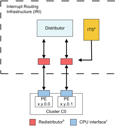
Image text
Interrupt Routing
Infrastructure (IRI)
Distributor ITS [a]
PE PE
x.y.0.0 x.y.0.1
Cluster C0
Redistributor [b] CPU interface [c]
b. There is one Redistributor per PE. c. There is one CPU interface per PE.
Figure 3-1 Interrupt Routing Infrastructure The CPU interface handles physical interrupts at all implemented Exception levels:
-
Interrupts that are translated into LPIs are optionally routed via the ITS to the Redistributor and the CPU interface.
-
PPIs are routed directly from the source to the local Redistributor.
-
SPIs are routed from the source through the Distributor to the target Redistributor and the associated CPU interface.
-
SGIs are generated by software through the CPU interface and Redistributor. They are then routed through the Distributor to one or more target Redistributors and the associated CPU interfaces.
In GICv3, the ITS is an optional component and translates events into physical LPIs. The architecture also supports direct LPIs that do not require the use of an ITS. Where LPIs are supported, it is IMPLEMENTATION DEFINED whether either:
-
Direct LPIs are supported by accessing the registers in the Redistributors.
-
LPI support is provided by the ITS.
An implementation must only support one of these methods.
In GICv4, the inclusion of at least one ITS is mandatory to provide support for the direct injection of virtual LPIs. Figure 3-2 shows the GIC partitioning in an implementation that includes an ITS.
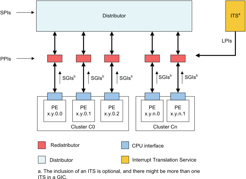
Image text
SPIs
Distributor ITS [a]
LPIs
PPIs
SGIs [b] SGIs [b] SGIs [b] SGIs [b] SGIs [b]
PE PE PE PE PE
x.y.0.0 x.y.0.1 x.y.0.2 x.y.n.0 x.y.n.1
Cluster C0 Cluster Cn
Redistributor CPU interface
Distributor Interrupt Translation Service
a. The inclusion of an ITS is optional, and there might be more than one
ITS in a GIC.
Figure 3-2 GIC logical partitioning with an ITS
The mechanism for communication between the ITS and the Redistributors is IMPLEMENTATION DEFINED.
The mechanism for communication between the CPU interfaces and the Redistributors is also IMPLEMENTATION DEFINED.
Note Arm recommends that an implementation uses the GIC Stream Protocol for communication between the CPU interfaces and the Redistributors, see Appendix A GIC Stream Protocol interface .
Figure 3-3 shows the GIC partitioning in an implementation that does not include an ITS and that supports direct LPIs. 3.1 The GIC logical components
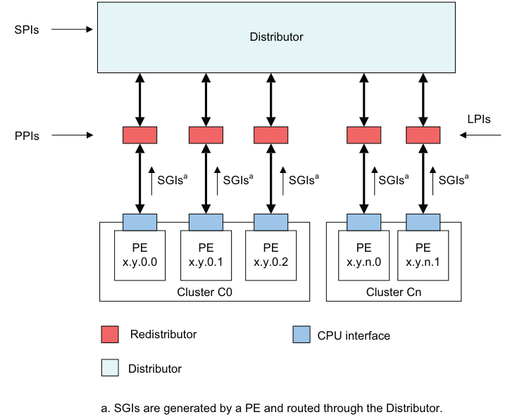
Image text
SPIs
Distributor
LPIs
PPIs
SGIs [a] SGIs [a] SGIs [a] SGIs [a] SGIs [a]
PE PE PE PE PE
x.y.0.0 x.y.0.1 x.y.0.2 x.y.n.0 x.y.n.1
Cluster C0 Cluster Cn
Redistributor CPU interface
Distributor
a. SGIs are generated by a PE and routed through the Distributor.
The following list describes the components that are depicted in Figure 3-2 in more detail:
Distributor
The Distributor performs interrupt prioritization and distribution of SPIs and SGIs to the Redistributors and CPU interfaces that are connected to the PEs in the system. GICD_CTLR provides global settings for:
-
Enabling affinity routing.
-
Disabling security.
-
Enabling Secure and Non-secure Group 1 interrupts.
-
Enabling Group 0 interrupts.
For SPIs, the Distributor provides a programming interface for:
-
Enabling or disabling SPIs.
-
Setting the priority level of each SPI.
-
Routing information for each SPI.
-
Setting each SPI to be level-sensitive or edge-triggered.
-
Generating message-based SPIs.
-
Assigning each SPI to an interrupt group.
-
Controlling the pending and active state of SPIs.
The Distributor registers are identified by the GICD_ prefix.
See Chapter 2 Distribution and Routing of Interrupts for more information.
Note When handling physical interrupts during legacy operation, the Distributor controls the configuration information for PPIs and SGIs. See Chapter 14 Legacy Operation and Asymmetric Configurations .
Interrupt translation service, ITS
The ITS is an OPTIONAL hardware mechanism in the GICv3 architecture that routes LPIs to the appropriate Redistributor. Software uses a command queue to configure an ITS. Table structures in memory that are associated with an ITS translate an EventID associated with a device into a pending INTID for a PE.
The ITS is not optional in GICv4, and all GICv4 implementations must include at least one ITS.
See The Interrupt Translation Service for more information.
Redistributor A Redistributor is the part of the IRI that is connected to the CPU interface of the PE. The Redistributor holds the control, prioritization, and pending information for all physical LPIs using data structures that are held in memory. Two registers in the Redistributor point to these data structures:
-
GICR_PROPBASER.
-
GICR_PENDBASER.
In GICv4, the Redistributor also includes registers to handle virtual LPIs that are forwarded by an ITS to a Redistributor and directly to a VM, without involving the hypervisor. This is referred to as a direct injection of virtual interrupts into a VM.
In GICv4, the Redistributors collectively host the control, prioritization, and pending information for all virtual LPIs using data structures that are held in memory. Two registers in the Redistributor point to these data structures:
-
GICR_VPROPBASER.
-
GICR_VPENDBASER.
In an implementation that supports LPIs but does not include an ITS, the GICR_* registers contain a simple memory-mapped interface to signal and control physical LPIs.
Redistributors provide a programming interface for:
-
Identifying, controlling, and configuring supported features to enable interrupts and interrupt routing of the implementation.
-
Enabling or disabling SGIs and PPIs.
-
Setting the priority level of SGIs and PPIs.
-
Setting each PPI to be level-sensitive or edge-triggered.
-
Assigning each SGI and PPI to an interrupt group.
-
Controlling the pending state of SGIs and PPIs.
-
Controlling the active state of SGIs and PPIs.
-
Power management support for the connected PE.
-
Where LPIs are supported, base address control for the data structures in memory that support the associated interrupt properties and their pending status.
-
Where GICv4 is supported, base address control for the data structures in memory that support the associated virtual interrupt properties and their pending status.
The Redistributor registers are identified by the GICR_ prefix.
See Affinity routing and The Distributor and Redistributors for more information about the Redistributor.
CPU interface
The GIC architecture supports a CPU interface that provides a register interface to a PE in the system. Each CPU interface provides a programming interface for:
-
General control and configuration to enable interrupt handling in accordance with the Security state and legacy support requirements of the implementation.
-
Acknowledging an interrupt.
-
Performing a priority drop.
-
Deactivation of an interrupt.
-
Setting an interrupt priority mask for the PE.
-
Defining the preemption policy for the PE.
-
Determining the highest priority pending interrupt for the PE.
The CPU interface has several components:
-
A component that allows a supervisory level of software to control the handling of physical interrupts. The registers that are associated with this are identified by the ICC_ prefix.
-
A component that allows a supervisory level of software to control the handling of virtual interrupts. The registers that are associated with this are identified by the ICV_ prefix.
-
A component that allows a hypervisor to control the set of pending interrupts. The registers that are associated with this are identified by the ICH_ prefix.
Note The System registers in the CPU interface are associated with software that is handling interrupts in the physical domain, or with execution at Non-secure EL1 as part of a VM. The configuration of HCR_EL2 determines whether the accesses are to the physical resources or the virtual resources.
The System registers accessible at EL2 that are used for controlling the list of active, pending, and active and pending, virtual interrupts for a PE are identified by the ICH_ prefix.
For more information on handling physical interrupts, see Chapter 4 Physical Interrupt Handling and Prioritization .
For more information on handling virtual interrupts, see Chapter 6 Virtual Interrupt Handling and Prioritization .
3.2 Interrupt bypass support
A CPU interface optionally includes interrupt signal bypass, so that, when the signaling of an interrupt by the interface is disabled, a legacy interrupt signal is passed to the interrupt request input on the PE, bypassing the GIC functionality.
It is IMPLEMENTATION DEFINED whether bypass is supported.
The controls to determine whether GICv3 FIQ and IRQ outputs or the bypass signals are used differ depending on whether System register access is enabled.
When System register access is enabled, bypass disable is controlled at the highest implemented Exception level using two bits in ICC_SRE_EL1, ICC_SRE_EL2, or ICC_SRE_EL3, as appropriate:
-
For FIQ bypass, this is the DFB bit.
-
For IRQ bypass, this is the DIB bit.
This bypass mechanism is used when System register access is enabled. For information about bypass support during legacy operation, see Legacy operation and bypass support .
The interrupt groups that are supported by the GIC are allocated to FIQs and IRQs, as described in Interrupt grouping . Interrupt groups must be disabled at the CPU interface when bypass is enabled, otherwise the behavior of the GICv3 implementation is UNPREDICTABLE. This means that:
-
ICC_IGRPEN0_EL1.Enable must have the value 0 when ICC_SRE_ELx.DFB == 0.
-
ICC_IGRPEN1_EL1.Enable must have the value 0 when ICC_SRE_ELx.DIB == 0.
For more information about enabling interrupts, see Enabling the distribution of interrupts .
For information about the behavior when System register access is not enabled, see Chapter 14 Legacy Operation and Asymmetric Configurations .
For FIQs, the following pseudocode determines the source for interrupt signaling to a PE.
if ICC_SRE_EL3.SRE == 1 then
    if ICC_SRE_EL3.DFB == 0 then
        if ICC_SRE_EL1.SRE Secure == 1 then
            BypassFIQsource
        else
            use legacy bypass support
    else
        use GICv3 FIQ output
else
    use legacy bypass support
For IRQs, the following pseudocode determines the source for interrupt signaling to a PE.
if ICC_SRE_EL3.SRE == 1 then
    if ICC_SRE_EL3.DIB == 0 then
        if ICC_SRE_EL1.SRE Secure == 1 then
            BypassIRQsource
        else
            use legacy bypass support
    else
        use GICv3 IRQ output
else
    use legacy bypass support
Chapter 4: Physical Interrupt Handling and Prioritization
This chapter describes the fundamental aspects of GIC interrupt handling and prioritization. It contains the following sections:
-
Interrupt lifecycle.
-
Locality-specific Peripheral Interrupts.
-
Private Peripheral Interrupts.
-
Software Generated Interrupts.
-
Shared Peripheral Interrupts.
-
Interrupt grouping.
-
Enabling the distribution of interrupts.
-
Interrupt prioritization.
4.1 Interrupt lifecycle
GIC interrupt handling is based on the GIC interrupt lifecycle, a series of high-level processes that apply to any interrupt using the GIC architecture. The interrupt lifecycle provides a basis for describing the detailed steps of the interrupt handling process. The GIC also maintains a state machine that controls interrupt state transitions during the lifecycle.
Figure 4-1 shows the GIC interrupt lifecycle for physical interrupts.
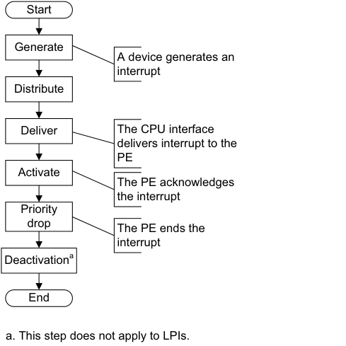
Image text
Start
Generate
A device generates an
interrupt
Distribute
Deliver The CPU interface
delivers interrupt to the
PE
Activate
The PE acknowledges
the interrupt
Priority
drop The PE ends the
interrupt
Deactivation [a]
End
a. This step does not apply to LPIs.
-
Generate interrupt. An interrupt is generated either by the peripheral or by software.
-
Distribute. The IRI performs interrupt grouping, interrupt prioritization, and controls the forwarding of interrupts to the CPU interfaces.
-
Deliver. A physical CPU interface delivers interrupts to the corresponding PE.
-
Activate. When software running on a PE acknowledges an interrupt, the GIC sets the highest active priority to that of the activated interrupt, and for SPIs, SGIs, and PPIs the interrupt becomes active.
-
Priority drop. Software running on the PE signals to the GIC that the highest priority interrupt has been handled to the point where the running priority can be dropped. The running priority then has the value that it had before the interrupt was acknowledged. This is the point where the end of interrupt is indicated by the interrupt handler. The end of the interrupt can be configured to also perform deactivation of the interrupt.
-
Deactivation. Deactivation clears the active state of the interrupt, and thereby allows the interrupt, when it is pending, to be taken again. Deactivation is not required for LPIs. Deactivation can be configured to occur at the same time as the priority drop, or it can be configured to occur later as the result of an explicit interrupt deactivation operation. This latter approach allows for software architectures where there is an advantage to separating interrupt handling into initial handling and scheduled handling.
4.1.1 Physical CPU interface
A CPU interface provides an interface to a PE that is connected to the GIC. Each CPU interface is connected to a single PE. A CPU interface receives pending interrupts prioritized by the IRI, and determines whether the interrupt is a member of a group that is enabled in the CPU interface and has sufficient priority to be signaled to the PE. At any time, the connected PE can determine the:
-
INTID of its highest priority pending interrupt, by reading ICC_HPPIR0_EL1 or ICC_HPPIR1_EL1.
-
The running priority of the CPU interface by reading ICC_RPR_EL1.
Note
The priority of the highest priority active interrupt for which there has not been a priority drop is also known as the running priority.
When an LPI is acknowledged, the pending state for the interrupt changes to not pending in the Redistributor. The Redistributor does not maintain an active state for LPIs.
When the PE acknowledges an SGI, a PPI, or an SPI at the CPU interface, the IRI changes the status of the interrupt to active if:
-
It is an edge-triggered interrupt, and another edge has not been detected since the interrupt was acknowledged.
-
It is a level-sensitive interrupt, and the level has been deasserted since the interrupt was acknowledged.
When the PE acknowledges an SGI, a PPI, or an SPI at the CPU interface, the IRI changes the status of the interrupt to active and pending if:
-
It is an edge-triggered interrupt, and another edge has been detected since the interrupt was acknowledged.
-
It is a level-sensitive interrupt, and the level has not been deasserted since the interrupt was acknowledged.
When the PE acknowledges an SGI, a PPI, or an SPI at the CPU interface, the CPU interface can signal another interrupt to the PE, to preempt interrupts that are active on the PE. If there is no pending interrupt with sufficient priority to be signaled to the PE, the interface deasserts the interrupt request signal to the PE.
The following stages of the interrupt lifecycle are described in the remainder of this section:
-
Activation .
-
Priority drop.
-
Deactivation.
The priority drop and deactivation can be performed as a single operation or can be split, as defined by ICC_CTLR_EL1.EOImode and ICC_CTLR_EL3.EOImode_EL3.
Activation
The interrupt handler reads ICC_IAR0_EL1 for Group 0 interrupts, and ICC_IAR1_EL1 for Group 1 interrupts, in the corresponding CPU interface to acknowledge the interrupt. This read returns either:
-
The INTID of the highest priority pending interrupt, if that interrupt is of sufficient priority for it to be signaled to the PE. This is the normal response to an interrupt acknowledge.
-
Under certain conditions, an INTID that indicates a special interrupt number, see INTIDs.
Whether a read of ICC_IAR0_EL1 and ICC_IAR1_EL1 returns a valid INTID depends on:
-
Which of the two registers is accessed.
-
The Security state of the PE.
-
Whether there is a pending interrupt of sufficient priority to be signaled to the PE, and if so, whether:
-
The highest priority pending interrupt is a Secure Group 1 or a Non-secure Group 1 interrupt.
-
Interrupt signaling is enabled for that interrupt group.
-
-
The Exception level at which the PE is executing.
All interrupts, when acknowledged, modify the Active Priorities Registers . See System register access to the Active Priorities registers. 4.1 Interrupt lifecycle
In certain circumstances, the value of SCR_EL3.NS affects the value returned when a PE acknowledges an interrupt. That is, when the PE is executing at EL3, a Secure read of ICC_IAR0_EL1 returns a special interrupt number that indicates the required Security state transition for the highest priority pending interrupt. Otherwise, the INTID is returned.
For SGIs in a multiprocessor implementation, the GIC uses the targeted list model, where the acknowledgement of an interrupt by one PE has no effect on the state of the interrupt on other CPU interfaces. When a PE acknowledges the interrupt, the pending state of the interrupt is cleared only for that PE. The interrupt remains pending for the other PEs.
The effects of reading ICC_IAR0_EL1 and ICC_IAR1_EL1 on the state of a returned INTID are not guaranteed to be visible until after the execution of a DSB.
Priority drop
After an interrupt has been acknowledged, a valid write to ICC_EOIR0_EL1 for Group 0 interrupts, or a valid write to ICC_EOIR1_EL1 for Group 1 interrupts, results in a priority drop.
A valid write to ICC_EOIR0_EL1 or ICC_EOIR1_EL1 to perform a priority drop is required for each acknowledged interrupt, even for LPIs which do not have an active state. A priority drop must be performed by the same PE that activated the interrupt.
Note A valid write is a write that is:
-
Not UNPREDICTABLE.
-
Not ignored.
-
Not writing an INTID that is either unsupported or within the range 1020-1023.
For each CPU interface, the GIC architecture requires the order of the valid writes to ICC_EOIR0_EL1 and ICC_EOIR1_EL1 to be the exact reverse of the order of the reads from ICC_IAR0_EL1 and ICC_IAR1_EL1, as shown in Figure 4-2.
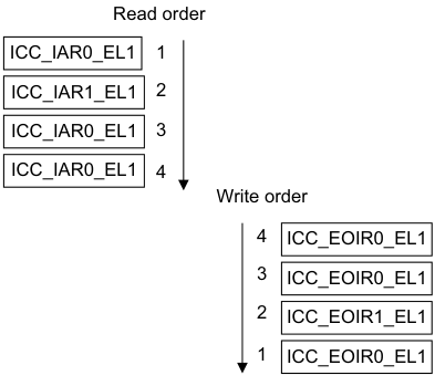
Image text
Read order
ICC_IAR0_EL1 1
ICC_IAR1_EL1 2
ICC_IAR0_EL1 3
ICC_IAR0_EL1 4
Write order
4 ICC_EOIR0_EL1
3 ICC_EOIR0_EL1
2 ICC_EOIR1_EL1
1 ICC_EOIR0_EL1
-
The priority of the highest-priority active interrupt for which there has been no write to ICC_EOIR0_EL1 or ICC_EOIR1_EL1.
-
The idle priority, 0xFF, if there is no active interrupt.
Note For compatibility with possible extensions to the GIC architecture specification, software must preserve the entire register value read from ICC_IAR0_EL1 and ICC_IAR1_EL1 when it acknowledges the interrupt, and use that entire value for the corresponding write to ICC_EOIR0_EL1 and ICC_EOIR1_EL1 by the same PE.
When GICD_CTLR.DS == 0:
-
A write to ICC_EOIR0_EL1 performs a priority drop for Group 0 interrupts.
-
A write to ICC_EOIR1_EL1 performs a priority drop for Non-secure Group 1 interrupts, if the PE is operating in Non-secure state or at EL3.
-
When operating in Secure state, a write to ICC_EOIR1_EL1 performs a priority drop for Secure Group 1 interrupts.
When GICD_CTLR.DS == 1:
-
A write to ICC_EOIR0_EL1 performs a priority drop for Group 0 interrupts.
-
A write to ICC_EOIR1_EL1 performs a priority drop for Group 1 interrupts.
Deactivation
PPIs, SGIs, and SPIs have an active state in the IRI and must be deactivated.
SGIs and PPIs must be deactivated by the PE that activated the interrupt. SPIs can be deactivated by a different PE.
Interrupt deactivation is required to change the state of an interrupt either:
-
From active and pending to pending.
-
From active to inactive.
Depending on the Exception level and Security state, ICC_CTLR_EL1.EOImode and
ICC_CTLR_EL3.EOImode_EL3 in the appropriate CPU Interface Control Register determine whether priority drop and interrupt deactivation happen together or separately:
-
The priority drop and interrupt deactivation happen together when ICC_CTLR_EL1.EOImode or ICC_CTLR_EL3.EOImode_EL3 in the CPU interface is 0, and the PE writes to ICC_EOIR0_EL1 or ICC_EOIR1_EL1. In this case a write to ICC_DIR_EL1 is not required.
-
The priority drop and interrupt deactivation are separated when ICC_CTLR_EL1.EOImode or ICC_CTLR_EL3.EOImode_EL3 in the CPU interface is 1, and the PE writes to ICC_EOIR0_EL1 or ICC_EOIR1_EL1. In this case:
-
The priority drop happens when the PE writes to ICC_EOIR0_EL1 or ICC_EOIR1_EL1.
-
Interrupt deactivation happens later, when the PE writes to ICC_DIR_EL1. A valid write to ICC_DIR_EL1 results in interrupt deactivation for a Group 0 or a Group 1 interrupt.
-
There are no ordering requirements for writes to ICC_DIR_EL1. If software writes to ICC_DIR_EL1 when the following conditions are true, the results are unpredictable:
-
The appropriate EOIMode bit is cleared to 0.
-
The ICC_CTLR_EL1.EOImode or ICC_CTLR_EL3.EOIMode_EL3 is set to 1 and there has not been a corresponding write to ICC_EOIR0_EL1 or ICC_EOIR1_EL1.
When ICC_CTLR_EL1.EOImode or ICC_CTLR_EL3.EOIMode_EL3 == 1 but the interrupt is not active in the Distributor, writes to ICC_DIR_EL1 must be ignored. If supported, an implementation might generate a system error. Table 4-1 shows how a write to ICC_EOIR0_EL1 or ICC_EOIR1_EL1 affects deactivation.
Table 4-1 Effect of writing to ICC_EOIR0_EL1 or ICC_EOIR1_EL1
| Access | ICC_CTLR_EL1.EOImode or ICC_CTLR_EL3.EOImode_EL3 | Identified interrupt | Effect |
|---|---|---|---|
| ICC_EOIR1_EL1 | 0 | Group 0 | Access ignored |
| ICC_EOIR0_EL1 | 0 | Group 0 | Interrupt deactivated |
| ICC_EOIR1_EL1 | 0 | Group 1 | Interrupt deactivated |
| ICC_EOIR0_EL1 | 0 | Group 1 | Access ignored |
| - | 1 | - | Interrupt remains active |
When GICD_CTLR.DS == 0, access to certain registers is restricted. See Interrupt grouping and security.
The following pseudocode determines whether EOImode is set for the current Exception level and Security state:
// EOImodeSet()
// ============

boolean EOImodeSet()

     if HaveEL(EL3) then
         // EL3 is implemented so return the value appropriate to the EL and security state
         if IsEL3OrMon() && ICC_SRE_EL3.SRE == '1'1 then
             // In EL3
             EOImode = ICC_CTLR_EL3.EOImode_EL3;

         elsif IsSecure() then
             EOImode = ICC_CTLR_EL3.EOImode_EL1S;

         else                                                  // Non-secure
              EOImode = ICC_CTLR_EL3.EOImode_EL1NS;
     else
         // No EL3 so return the value from ICC_CTLR_EL1
         EOImode = ICC_CTLR_EL1.EOImode;

     return EOImode == '1';
Effect of Security states on writes to ICC_DIR_EL1
The effect of a write to ICC_DIR_EL1 depends on whether the GIC supports one or two Security states:
-
If GICD_CTLR.DS == 0, a valid:
- Secure write to ICC_DIR_EL1 deactivates the specified interrupt, regardless of whether that interrupt is a Group 0 or a Group 1 interrupt.- Non-secure write to ICC_DIR_EL1 deactivates the specified interrupt only if that interrupt is a Non-secure Group 1 interrupt.
-
If GICD_CTLR.DS == 1, a valid write to ICC_DIR_EL1 deactivates the specified interrupt, regardless of whether that interrupt is a Group 0 or Group 1 interrupt. Table 4-2 shows the behavior of valid writes to ICC_DIR_EL1. In an implementation that supports only a single Security state, valid writes have the behavior shown for Secure writes to ICC_DIR_EL1.
Table 4-2 Behavior of writes to ICC_DIR_EL1
| Security state and Exception level of writes to ICC_DIR_EL1 | Interrupt group | GICD_CTLR.DS | SCR_EL3.IRQ | SCR_EL3.FIQ | Effect |
|---|---|---|---|---|---|
| EL3 | x | x | x | x | Interrupt is deactivated |
| Secure EL1 or Secure EL2 | Group 0 | x | x | 0 | Interrupt is deactivated |
| Secure EL1 or Secure EL2 | Group 0 | x | x | 1 | Write is ignored |
| Secure EL1 or Secure EL2 | Group 1 | x | 0 | x | Interrupt is deactivated |
| Secure EL1 or Secure EL2 | Group 1 | x | 1 | x | Write is ignored |
| EL2 or Non-secure EL1 | Group 0 or Secure Group 1 | 0 | x | x | Write is ignored |
| EL2 or Non-secure EL1 | Group 0 | 1 | x | 0 | Interrupt is deactivated |
| EL2 or Non-secure EL1 | Group 0 | 1 | x | 1 | Write is ignored |
| EL2 or Non-secure EL1 | Non-secure Group 1 | 0 | 0 | x | Interrupt is deactivated |
| EL2 or Non-secure EL1 | Non-secure Group 1 | 0 | 1 | x | Write is ignored |
| EL2 or Non-secure EL1 | Group 1 | 1 | 0 | x | Interrupt is deactivated |
| EL2 or Non-secure EL1 | Group 1 | 1 | 1 | x | Write is ignored |
Secure EL2 can only be entered when SCR_EL3.EEL2 == 1.
4.1.2 Interrupt handling state machine
The GIC maintains a state machine for each supported interrupt. The possible states of an interrupt are:
-
Inactive.
-
Pending.
-
Active.
-
Active and pending.
PPIs, SGIs, and SPIs can have an active and pending state. Interrupts that are active and pending are never signaled to a connected PE. LPIs have a pending state that is held in memory associated with a Redistributor, and therefore a PE. This also applies to directly injected virtual LPIs, see About GICv4.0 virtual Locality-specific Peripheral Interrupt support.
Note There is no active or active and pending state for LPIs.
Figure 4-3 shows an instance of the interrupt handling state machine, and the possible state transitions.
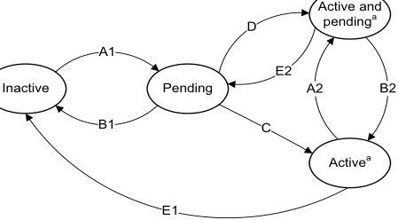
Image text
Active and
D pending [a]
A1
E2
Inactive Pending A2 B2
B1 C
Active [a]
E1
a. Not applicable for SGIs when GICD_CTLR.nASSGIreq==1,
and for LPIs.
Figure 4-3 Interrupt handling state machine
Note LPIs do not have an active state in the Redistributor, but do require an active priority in the CPU interface. See Chapter 5 Locality-specific Peripheral Interrupts and the ITS for more information.
Arm expects hardware implementations to report GICD_TYPER2.nASSGIcap==0, indicating that GICD_CTLR.nASSGIreq is RES0.
When interrupt forwarding by the Distributor and interrupt signaling by the CPU interface are enabled, the conditions that cause each of the state transitions are as follows:
Transition A1 or A2, add pending state
This transition occurs when the interrupt becomes pending, either as a result of the peripheral generating the interrupt or as result of software generating the interrupt.
Transition B1 or B2, remove pending state
This transition occurs when the interrupt has been deasserted by the peripheral, if the interrupt is a level-sensitive interrupt, or when software has changed the pending state.
For LPIs, it also occurs on acknowledgement of the interrupt.
Transition C, pending to active
This transition occurs on acknowledgement of the interrupt by the PE for edge-triggered SPIs, SGIs, and PPIs.
For SPIs, SGIs, and PPIs, this transition occurs when software reads an INTID value from ICC_IAR0_EL1 or ICC_IAR1_EL1.
Transition D, pending to active and pending
This transition occurs on acknowledgement of the interrupt by the PE for level-sensitive SPIs, SGIs, and PPIs.
Transition E1 or E2, remove active state
This transition occurs when software deactivates an interrupt for SPIs, SGIs, and PPIs.
4.2 Locality-specific Peripheral Interrupts
LPIs are targeted peripheral interrupts that are routed to a specific PE within the affinity hierarchy. In a system where two Security states are enabled, LPIs are always Non-secure Group 1 interrupts. LPIs only support edge-triggered behavior. For more information about LPIs, see LPIs.
4.3 Private Peripheral Interrupts
PPIs are interrupts that target a single, specific PE, and different PEs can use the same INTID to indicate different events. PPIs can be Group 0 interrupts, Secure Group 1 interrupts, or Non-secure Group 1 interrupts. They can support either edge-triggered or level-sensitive behavior.
An optional extended PPI range uses INTIDs 1056 - 1119. This range of PPIs is not available when the GIC is operating in legacy mode. GICR_TYPER.PPInum indicates whether the extended PPI range is supported or not.
Note Commonly, Arm expects that PPIs are used by different instances of the same interrupt source on each PE, thereby allowing a common INTID to be used for PE specific events, such as the interrupts from a private timer.
4.4 Software Generated Interrupts
SGIs are typically used for inter-processor communication, and are generated by a write to an SGI register in the GIC. SGIs can be either Group 0 or Group 1 interrupts, and they can support only edge-triggered behavior.
The registers associated with the generation of SGIs are part of the CPU interface:
-
A PE generates a Group 1 SGI by writing to ICC_SGI1R_EL1 or ICC_ASGI1R_EL1.
-
A PE generates a Group 0 SGI by writing to ICC_SGI0R_EL1.
-
Routing information is supplied as the bitfield value in the write to the register that generated the SGI. The SGI can be routed to:
-
The group of PEs specified by a.b.c.targetlist. This can include the originating PE.
-
All participating PEs in the system, excluding the originating PE.
-
See Routing SPIs and SGIs by PE affinity for more information.
ICC_SGI1R_EL1 allows software executing in a Secure state to generate Secure Group 1 SGIs.
ICC_SGI1R_EL1 allows software executing in a Non-secure state to generate Non-secure Group 1 SGIs.
ICC_ASGI1R_EL1 allows software executing in a Secure state to generate Non-secure Group 1 SGIs.
ICC_ASGI1R_EL1 allows software executing in a Non-secure state to generate Secure Group 1 SGIs, if permitted by the settings of GICR_NSACR in the Redistributor corresponding to the target PE.
ICC_SGI0R_EL1 allows software executing in Secure state to generate Group 0 SGIs.
ICC_SGI0R_EL1 allows software executing in Non-secure state to generate Group 0 SGIs, if permitted by the settings of GICR_NSACR in the Redistributor corresponding to the target PE.
For more information about the use of control registers to forward SGIs to a target PE, see Table 12-14.
4.5 Shared Peripheral Interrupts
SPIs are peripheral interrupts that the Distributor can route to a specified PE that can handle the interrupt, or to a PE that is one of a group of PEs in the system that has been configured to accept this type of interrupt. SPIs can be either Group 0 or Group 1 interrupts, and they can support either edge-triggered or level-sensitive behavior.
An optional extended SPI range uses INTIDs 4096 - 5119. This range of SPIs is not available when the GIC is operating in legacy mode. GICD_TYPER.ESPI indicates whether the extended SPI range is supported or not.
SPIs can be either wired-based or message-based interrupts.
Support for message-based SPIs is optional, and can be discovered through GICD_TYPER.MBIS. Message-based SPIs can be:
-
Generated by a write to GICD_SETSPI_NSR or GICD_SETSPI_SR
-
Cleared by a write to GICD_CLRSPI_NSR or GICD_CLRSPI_SR.
The effect of a write to these registers depends on whether the targeted SPI is configured to be an edge-triggered or a level-sensitive interrupt:
-
For an edge-triggered interrupt, a write to GICD_SETSPI_NSR or GICD_SETSPI_SR sets the interrupt pending. The interrupt is no longer pending when it is activated, or when it is cleared by a write to GICD_CLRSPI_NSR, GICD_CLRSPI_SR, or GICD_ICPENDR
. -
For a level-sensitive interrupt, a write to GICD_SETSPI_NSR or GICD_SETSPI_SR sets the interrupt pending. It remains pending until it is deasserted by a write to GICD_CLRSPI_NSR or GICD_CLRSPI_SR. If the interrupt is activated between the time it is asserted by a write to GICD_SETSPI_NSR or GICD_SETSPI_SR and the time it is deactivated by a write to GICD_CLRSPI_NSR or GICD_CLRSPI_SR, then the interrupt becomes active and pending.
-
It is IMPLEMENTATION DEFINED for a level-sensitive interrupt whether a write to GICD_ICPENDR
has any effect on an interrupt that has been set pending by a write to GICD_SETSPI_NSR or GICD_SETSPI_SR, or whether a write to GICD_CLRSPI_NSR or GICD_CLRSPI_SR has any effect on an interrupt that has been set pending by a write GICD_ISPENDR . -
It is IMPLEMENTATION DEFINED whether acknowledging an interrupt that was set pending by a write to GICD_ISPENDR
clears the pending state.
-
-
Changing the configuration of an interrupt from level-sensitive to edge-triggered, or from edge-triggered to level-sensitive, when there is a pending interrupt, leaves the interrupt in an UNKNOWN state.
Figure 4-4 shows how message-based interrupt requests can trigger SPIs.
| Wire-based | Wire-based | Wire-based | Wire-based | Wire-based | Wire-based | SPIs | SPIs | SPIs | ||||||||||||||||||||||||
|---|---|---|---|---|---|---|---|---|---|---|---|---|---|---|---|---|---|---|---|---|---|---|---|---|---|---|---|---|---|---|---|---|
| Message- | Distributor | |||||||||||||||||||||||||||||||
| based SPIs | GICD_SETSPI_SR registers | GICD_SETSPI_NSR | registers | |||||||||||||||||||||||||||||
| GICD_CLRSPI_SR registers | GICD_CLRSPI_NSR | registers | ||||||||||||||||||||||||||||||
| x.y.0.0 | PE Redistributor | Cluster C0 | x.y.0.1 | PE | x.y.0.2 | PE | CPU interface | x.y.n.0 | PE | Cluster | PE x.y.n.1 Cn |
Figure 4-4 Triggering SPIs
4.6 Interrupt grouping
GICv3 uses interrupt grouping as a mechanism to align interrupt handling with the Armv8 Exception model and Security model.
In a system with two Security states, an interrupt is configured as one of the following:
-
A Group 0 physical interrupt:
- Arm expects these interrupts to be handled at EL3.
-
A Secure Group 1 physical interrupt:
- Arm expects these interrupts to be handled at Secure EL1 or Secure EL2 in a system using Secure virtualization.
-
A Non-secure Group 1 physical interrupt:
- Arm expects these interrupts to be handled at Non-secure EL2 in systems using virtualization, or at Non-secure EL1 in systems not using virtualization.
In a system with one Security state an interrupt is configured to be either:
-
Group 0.
-
Group 1.
At the System level, GICD_CTLR.DS indicates if the GIC is configured with one or two Security states. For more information about Security, see Interrupt grouping and security.
These interrupt groups are mapped onto the Armv8 FIQ and IRQ exceptions, see Interrupt assignment to IRQ and FIQ signals.
GICD_IGROUPR
GICR_IGROUPR0 and GICR_IGRPMODR0 configure the interrupt group for SGIs and PPIs, and GICR_IGROUPR
Note
When GICD_CTLR.DS == 0, LPIs are always Non-secure Group 1 interrupts. When GICD_CTLR.DS == 1, LPIs are always Group 1 interrupts.
System registers control and configure Group 0 and Group 1 interrupts:
-
For Group 0 interrupts, software uses: — ICC_IAR0_EL1 to read a Group 0 INTID on an interrupt acknowledge.
-
ICC_EOIR0_EL1 to write a Group 0 interrupt completion.
-
ICC_BPR0_EL1 to configure the binary point for Group 0 prioritization. This register is also used for Group 1 prioritization when ICC_CTLR_EL1.CBPR == 1.
-
ICC_HPPIR0_EL1 to read the highest Group 0 interrupt that is currently pending.
-
ICC_IGRPEN0_EL1 to enable Group 0 interrupts at the CPU interface.
-
-
For Group 1 interrupts, software uses:
-
ICC_IAR1_EL1 to read a Group 1 INTID on an interrupt acknowledge.
-
ICC_EOIR1_EL1 to write a Group 1 interrupt completion.
-
ICC_BPR1_EL1 to configure the binary point for Group 1 prioritization for the current Security state.
-
ICC_HPPIR1_EL1 to read the highest Group 1 interrupt that is currently pending.
-
ICC_IGRPEN1_EL1 to enable Group 1 interrupts for the target Security state of the interrupt.
-
In a system with two Security states, Group 0 interrupts are always Secure. For more information about grouping and Security, see Interrupt grouping and security.
4.6.1 Interrupt grouping and security
The Arm architecture provides two Security states, each with an associated physical memory address space:
-
Secure state.
-
Non-secure state.
A software hierarchy of user and privileged code can execute in either state, and software executing in Non-secure state can only access Secure state through a system call to the Secure monitor. The GIC architecture supports the routing and handling of interrupts associated with both Security states.
GICD_CTLR.DS indicates whether a GIC is configured to support the Armv8-A Security model. This configuration affects:
-
Register access, see GIC System register access.
-
The interrupt groups that are supported.
When GICD_CTLR.DS == 0:
-
The GIC supports two Security states, Secure state and Non-secure state.
-
The GIC supports three interrupt groups:
- Group 0. - Secure Group 1.- Non-secure Group 1.
-
Both the Security state and GICR_NSACR determine whether an SGI can be generated.
-
The Security state is checked during:
- Configuration of an interrupt. - Acknowledgement of an interrupt.-
Priority drop.
-
Deactivation.
-
-
Secure Group 1 interrupts are treated as Group 0 by a CPU interface if:
-
The PE does not implement EL3.
-
ICC_SRE_EL1(S).SRE == 0.
-
When GICD_CTLR.DS == 1:
-
The GIC supports only a single Security state. This can be either Secure state or Non-secure state.
-
The GIC supports two interrupt groups:
-
Group 0.
-
Group 1.
-
-
SGIs can be generated regardless of the settings in GICR_NSACR.
-
The Security state is not checked during:
-
Configuration of an interrupt.
-
Acknowledgement of an interrupt.
-
Priority drop.
-
-
Deactivation.
In a multiprocessor system, one or more PEs within the system might support accesses to resources that are available only in Secure state, or accesses to resources that are available only in Non-secure state. It is a programming error if software configures:
-
A Group 0 or Secure Group1 interrupt to be forwarded to a PE that only supports Non-secure state.
-
A Non-secure Group1 interrupt to be forwarded to a PE that only supports Secure state.
There is a dedicated register for the priority grouping for each interrupt group, ICC_BPR0_EL1 for Group 0 interrupts and ICC_BPR1_EL1 for Group 1 interrupts. However, it is possible to configure a common Binary Point Register for both groups using:
-
ICC_CTLR_EL1.CBPR.
-
ICC_CTLR_EL3.CBPR_EL1NS and ICC_CTLR_EL3.CBPR_EL1S for an independent common Binary Point Register configuration of Non-secure Group 1 and Secure Group 1 interrupts. For information about interrupt grouping and legacy operation, see Chapter 14 Legacy Operation and Asymmetric Configurations .
4.6.2 Interrupt assignment to IRQ and FIQ signals
This subsection applies to implementations in which affinity routing is enabled.
A Group 0 physical interrupt, when it is the highest priority pending interrupt and has sufficient priority, is always signaled as an FIQ.
A Group 1 physical interrupt, when it is the highest priority pending interrupt and has sufficient priority, is signaled as an FIQ if either of the following conditions is true, otherwise it is signaled as an IRQ:
-
It is an interrupt for the other Security state, that is, the Security state in which the PE is not executing.
-
• The PE is executing at EL3.
Table 4-3 summarizes the signaling of interrupts when EL3 is using AArch64 state.
Table 4-3 Interrupt signals for two Security states when EL3 is using AArch64 state
| Current Exception level | Group 0 interrupts | Secure Group 1 interrupts | Non-secure Group 1 interrupts |
|---|---|---|---|
| Secure EL1 or EL0 or EL2 | FIQ | IRQ | FIQ |
| Non-secure EL1 or EL0, or Non-secure EL2 | FIQ | FIQ | IRQ |
| EL3 | FIQ | FIQ | FIQ |
Table 4-4 summarizes the signaling of interrupts when EL3 is using AArch32 state. Secure EL2 is not present when EL3 is using AArch32 state.
Table 4-4 Interrupt signals for two Security states when EL3 is using AArch32 state
| Current Exception level | Group 0 interrupts | Secure Group 1 interrupts | Non-secure Group 1 interrupts |
|---|---|---|---|
| Secure EL0 | FIQ | IRQ | FIQ |
| Non-secure EL1 or EL0, or Non-secure EL2 | FIQ | FIQ | IRQ |
| EL3 | FIQ | IRQ | FIQ |
Table 4-5 summarizes the signaling of interrupts in systems that support only a single Security state, that is where EL3 is not implemented or when GICD_CTLR.DS == 1.
Table 4-5 Interrupt signals for a single Security state
| Current Exception level | Group 0 interrupts | Group 1 interrupts |
|---|---|---|
| Any | FIQ | IRQ |
The assertion and de-assertion of IRQs and FIQs are affected by the current Exception level and Security state of the PE. As part of the Context Synchronization that occurs as the result of taking or returning from an exception, the CPU interface ensures that IRQ and FIQ are both appropriately asserted or deasserted for the Exception level and Security state that the PE is entering.
Note For the effects of GICC_CTLR.FIQEn on interrupt signaling in asymmetric configurations, see The asymmetric configuration.
4.6.3 Interrupt routing and System register access
When executing in AArch64 state, interrupt routing to an Exception level is controlled by the following bits:
-
SCR_EL3.FIQ, SCR_EL3.NS, and HCR_EL2.FMO control FIQs.
-
SCR_EL3.IRQ, SCR_EL3.NS, and HCR_EL2.IMO control IRQs.
This routing also controls the Exception level at which the EL1 CPU interface System registers that control and acknowledge interrupts are accessible. This applies to:
-
ICC_IAR0_EL1, ICC_EOIR0_EL1, ICC_HPPIR0_EL1, ICC_BPR0_EL1, ICC_AP0R
_EL1 and ICC_IGRPEN0_EL1. These are the registers that are associated with Group 0 interrupts. -
ICC_IAR1_EL1, ICC_EOIR1_EL1, ICC_HPPIR1_EL1, ICC_BPR1_EL1, ICC_AP1R
_EL1 and ICC_IGRPEN1_EL1. These are the registers that are associated with Group 1 interrupts. -
ICC_SGI0R_EL1, ICC_SGI1R_EL1, ICC_ASGI1R_EL1, ICC_CTLR_EL1, ICC_DIR_EL1, ICC_PMR_EL1, and ICC_RPR_EL1. These are the Common registers.
When (SCR_EL3.NS == 1 || SCR_EL3.EEL2== 1) && (HCR_EL2.FMO ==1 || HCR_EL2.IMO == 1)), accesses at EL1 are virtual accesses. Virtual accesses to ICC_SGI0R_EL1, ICC_SGI1R_EL1, and ICC_ASGI1R_EL1 always generate a Trap exception that is taken to EL2. Where a Distributor supports two Security states a PE might not implement EL2 or EL3. Table 4-6 shows the configurations that are supported in these cases.
Table 4-6 Supported configurations when EL3 is not implemented
| Distributor | EL3 | EL2 | Security State | Description |
|---|---|---|---|---|
| Two Security states, GICD_CTLR.DS == 0 | No | - | Non-secure | The PE is always Non-secure and can only receive Non-secure Group 1 interrupts. The PE must behave as if software had: Set ICC_SRE_EL3.Enable to 1; Set ICC_SRE_EL3.DFB to 1; Set SCR_EL3.FIQ to 1; Cleared SCR_EL3.IRQ to 0; Set SCR_EL3.NS to 1; Cleared ICC_IGRPEN0_EL1.Enable to 0; Set the Secure copy of ICC_IGRPEN1_EL1.Enable to 0. |
| Two Security states, GICD_CTLR.DS == 0 | No | No | Secure | The PE is always Secure and can only receive Group 0 and Secure Group 1 interrupts. The PE must behave as if software had: Set ICC_SRE_EL3.Enable to 1; Cleared SCR_EL3.FIQ to 0; Cleared SCR_EL3.IRQ to 0; Cleared SCR_EL3.NS to 0; Cleared the Non-secure copy of ICC_IGRPEN1_EL1.Enable to 0. |
| One Security state, or two Security states with GICD_CTLR.DS == 1 | No | - | - | The Distributor and all PEs are always in a single Security state, and can receive Group 0 and Group 1 interrupts. All PEs must behave as if software had: Set ICC_SRE_EL3.Enable to 1; Cleared SCR_EL3.FIQ to 0; Cleared SCR_EL3.IRQ to 0; Set SCR_EL3.NS to 1. |
4.7 Enabling the distribution of interrupts
The following control bits enable and disable the distribution of interrupts:
-
GICD_CTLR.EnableGrp1S.
-
GICD_CTLR.EnableGrp1NS.
-
GICD_CTLR.EnableGrp0.
The following control bits enable and disable the distribution of interrupt groups at the CPU interface:
-
ICC_IGRPEN0_EL1.Enable for Group 0 interrupts.
-
ICC_IGRPEN1_EL1.Enable for Group 1 interrupts.
Note
-
There is a Secure and a Non-secure copy of this register.
-
ICC_IGRPEN1_EL3.{EnableGrp1S, EnableGrp1NS}.
Physical LPIs are enabled by a write to GICR_CTLR.EnableLPIs.
4.7.1 Enabling individual interrupts
PPIs
PPIs can be enabled and disabled by writing to GICR_ISENABLER0 and GICR_ICENABLER0 when affinity routing is enabled for the Security state of the interrupt. Individual PPIs can also be enabled and disabled by writing to GICD_ISENABLER
PPIs in the optional, extended PPI range are enabled and disabled by writing to GICR_ISENABLER
SPIs
Individual SPIs can be enabled and disabled by writing to GICD_ISENABLER
SPIs in the optional, extended SPI range are enabled and disabled by writing to GICD_ISENABLER
SGIs
SGIs can be enabled and disabled by writing to GICR_ISENABLER0 and GICR_ICENABLER0 when affinity routing is enabled. Individual SGIs can also be enabled and disabled by writing to GICD_ISENABLER
Note Whether SGIs are permanently enabled, or can be enabled and disabled by writes to GICR_ISENABLER0 and GICR_ICENABLER0, is IMPLEMENTATION DEFINED.
LPIs
Individual LPIs can be enabled by setting the enable bits programmed in the LPI Configuration table. For more information about enabling LPIs using the LPI Configuration tables, see LPI Configuration tables.
4.7.2 Interaction of group and individual interrupt enables
The GICD_* and GICR_* registers determine, at any moment in time, the highest priority pending interrupt that the hardware is aware of for each target PE. This interrupt is presented to the CPU interface of a PE to evaluate whether it is to be signaled to the PE. The enabling of the interrupts affects this evaluation as follows:
-
A pending interrupt that is individually disabled in the GICD_* or GICR_* registers is not one which is considered in the determination of the highest priority pending interrupt, and so cannot be signaled to the PE.
-
A pending interrupt that is individually enabled in the GICD_* or GICR_* registers, but is a member of a group that is disabled in GICD_CTLR, is not one that is considered in the determination of the highest priority pending interrupt, and so cannot be signaled to the PE.
-
A pending 1 of N interrupt that is individually enabled in the GICD_* registers and is a member of a group that is enabled in GICD_CTLR, but is a member of a group that is disabled in ICC_IGRPEN0_EL1, ICC_IGRPEN1_EL1, or ICC_IGRPEN1_EL3 for a PE, cannot be selected for that PE. Such an interrupt is not considered in the determination of the highest priority pending interrupt and so cannot be signaled to the PE.
-
For a pending direct interrupt that is individually enabled in the GICD_* or GICR_* registers and is a member of a group that is enabled in GICD_CTLR, but is a member of a group that is disabled in ICC_IGRPEN0_EL1, ICC_IGRPEN1_EL1, or ICC_IGRPEN1_EL3, it is IMPLEMENTATION DEFINED whether or not the interrupt is considered in the determination of the highest priority pending interrupt. If it is determined to be the highest priority pending interrupt, the interrupt is not signaled to the PE, but will mask a lower priority pending interrupt that is a member of a group that is enabled in ICC_IGRPEN0_EL1, ICC_IGRPEN1_EL1, or ICC_IGRPEN1_EL3.
LPIs are enabled individually in the LPI Configuration tables, see LPI Configuration tables.
4.7.3 Effect of disabling interrupts
Disabling an interrupt by writing to the appropriate GICD_ICENABLER
If GICD_CTLR.EnableGrp0, GICD_CTLR.EnableGrp1S, and GICD_CTLR.EnableGrp1NS are all cleared to 0, it is IMPLEMENTATION DEFINED whether:
-
An edge-triggered interrupt signal moves the interrupt to the pending state.
-
SGIs can be set pending by writing to GICD_SGIR, ICC_SGI0R_EL1, ICC_SGI1R_EL1, or ICC_ASGI1R_EL1.
If an interrupt is pending on a CPU interface when the corresponding GICD_CTLR.EnableGrp0, GICD_CTLR.EnableGrp1NS, or GICD_CTLR.EnableGrp1S bit is written from 1 to 0, then the interrupt must be retrieved from the CPU interface.
Note This might have no effect on the forwarded interrupt if it has already been activated.
If an interrupt is pending on a CPU interface when software writes ICC_IGRPEN0_EL1.Enable, ICC_IGRPEN0_EL1, ICC_IGRPEN1_EL1.Enable, or ICC_IGRPEN1_EL3.Enable from 1 to 0, the interrupt must be released by the CPU interface to allow the Distributor to forward the interrupt to a different PE.
4.8 Interrupt prioritization
This section describes interrupt prioritization in the GIC architecture. Prioritization describes the:
-
Configuration and control of interrupt priority.
-
Order of execution of pending interrupts.
-
Determination of when interrupts are visible to a target PE, including:
-
Interrupt priority masking.
-
Priority grouping.
-
Preemption of an active interrupt.
-
Software configures interrupt prioritization in the GIC by assigning a priority value to each interrupt source. Priority values are an 8-bit unsigned binary number. A GIC implementation that supports two Security states must implement a minimum of 32 and a maximum of 256 levels of physical priority. A GIC implementation that supports only a single Security state must implement a minimum of 16 and a maximum of 256 levels of physical priority. If the GIC implements fewer than 256 priority levels, the low-order bits of the priority fields are RAZ/WI. This means that the number of implemented priority field bits is IMPLEMENTATION DEFINED, in the range 4-8. Table 4-7 shows the relation between the priority field bits and the number of priority levels supported by an implementation.
Table 4-7 Effect of not implementing some priority field bits
| Implemented priority bits | Possible | priority field values | Number of priority levels |
|---|---|---|---|
| [7:0] | 0x00-0xFF | (0-255), all values | 256 |
| [7:1] | 0x00-0xFE, | (0-254), even values only | 128 |
| [7:2] | 0x00-0xFC | (0-252), in steps of 4 | 64 |
| [7:3] | 0x00-0xF8 | (0-248), in steps of 8 | 32 |
| [7:4] | 0x00-0xF0 | (0-240), in steps of 16 | 16 |
In the GIC prioritization scheme, lower numbers have higher priority. This means that the lower the assigned priority value, the higher the priority of the interrupt. Priority field value 0 always indicates the highest possible interrupt priority, and the lowest priority value depends on the number of implemented priority levels.
The GICD_IPRIORITYR
In a multiprocessor implementation, the GICR_IPRIORITYR
LPI Configuration tables and LPI Pending tables in memory store LPI priority information and pending status, see LPI Configuration tables and LPI Pending tables.
The GIC security model provides Secure and Non-secure accesses to the interrupt priority settings.The Non-secure accesses can configure interrupts only in the lower priority half of the supported priority values. Therefore, if the GIC implements 32 priority values, Non-secure accesses see only 16 priority values. See Software accesses of interrupt priority for more information.
To determine the number of priority bits implemented for SPIs, software can write 0xFF to a writable GICD_IPRIORITYR
To determine the number of priority bits implemented for SGIs and PPIs, software can write 0xFF to the GICR_IPRIORITYR
The GIC architecture does not require all PEs in the system to use the same number of priority bits to control interrupt priority. In a multiprocessor implementation, ICC_CTLR_EL1.PRIbits and ICC_CTLR_EL3.PRIbits indicate the number of priority bits implemented, independently for each target PE.
Note Arm recommends that implementations support the same number of priority bits for each PE.
For information about the priority range supported for virtual interrupts, see Chapter 6 Virtual Interrupt Handling and Prioritization .
Note Arm recommends that, before checking the priority range in this way:
-
For a peripheral interrupt, software first disables the interrupt.
-
For an SGI, software first checks that the interrupt is inactive.
If, on a particular CPU interface, multiple pending interrupts have the same priority, and have sufficient priority for the interface to signal them to the PE, it is IMPLEMENTATION DEFINED how the interface selects which interrupt to signal.
GICv3 guarantees that the highest priority, unmasked, enabled interrupt will be delivered to a target PE in finite time.
There is no guarantee that higher priority interrupts will always be taken before lower priority interrupts, although this will generally be the case.
The remainder of this section describes:
-
Non-secure accesses to register fields for Secure interrupt priorities .
-
Priority grouping.
-
System register access to the Active Priorities registers.
-
Preemption.
-
Priority masking.
-
Software accesses of interrupt priority.
-
Changing the priority of enabled PPIs, SGIs, and SPIs.
4.8.1 Non-secure accesses to register fields for Secure interrupt priorities
When GICD_CTLR.DS == 0, the GIC supports the use of:
-
Group 0 interrupts as Secure interrupts.
-
Secure Group 1 interrupts.
-
Non-secure Group 1 interrupts.
In order to support the Armv8 Security model the register fields associated with Secure interrupts are RAZ/WI for Non-secure accesses. In addition, the following rules apply:
For Non-secure access to a priority field in GICx_IPRIORITYR:
If the priority field corresponds to a Non-secure Group 1 interrupt in Software accesses of interrupt priority:
-
For SPIs, the priority field is determined by GICD_IPRIORITYR
or GICD_IPRIORITYR E. -
For PPIs and SGIs, the priority field is determined by GICR_IPRIORITYR
or GICR_IPRIORITYR E.
For Non-secure access to ICC_PMR_EL1 and ICC_RPR_EL1 when SCR_EL3.FIQ == 1:
-
If the current priority mask value is in the range of 0x00-0x7F:
- A read access returns the value 0x00.
-
The GIC ignores a write access to ICC_PMR_EL1.
-
If the current priority mask value is in the range of 0x80-0xFF:
-
A read access returns the Non-secure read of the current value.
-
A write access to ICC_PMR_EL1 succeeds, based on the Non-secure read of the priority mask value written to the register.
Note
This means a Non-secure write cannot set a priority mask value in the range of 0x00-0x7F.
For Non-secure access to ICC_PMR_EL1 and ICC_RPR_EL1 when SCR_EL3.FIQ == 0:
The Secure, unshifted view applies.
AArch64 functions provides pseudocode that describes accesses to the following System registers in a GIC that supports two Security states:
-
ICC_PMR_EL1.
-
ICC_RPR_EL1.
4.8.2 Priority grouping
Priority grouping uses the following Binary Point Registers :
-
ICC_BPR0_EL1 for Group 0 interrupts. This register is available in all GIC implementations.
-
A Non-secure copy of ICC_BPR1_EL1 for Non-secure Group 1 interrupts. If an implementation supports two Security states, there is a Secure and a Non-secure copy of this register. If an implementation supports only one Security state, there is only one copy of this register
-
A Secure copy of ICC_BPR1_EL1 for Secure Group 1 interrupts. This register is available only in a GIC implementation that supports two Security states.
The Binary Point Registers split a priority value into two fields, the group priority and the subpriority . When determining preemption, all interrupts with the same group priority are considered to have the same priority, regardless of the subpriority.
Where multiple pending interrupts have the same group priority, the GIC uses the subpriority field to resolve the priority within a group. Where two or more pending interrupts in a group have the same subpriority, how the GIC selects between the interrupts is implementation specific.
The GIC uses the group priority field to determine whether a pending interrupt has sufficient priority to preempt execution on a PE, as follows:
-
The value of the group priority field for the interrupt must be lower than the value of the running priority of the PE. The running priority is the group priority of the highest priority active interrupt that has not received a priority drop on that PE.
-
The value of the priority for the interrupt must be lower than the value of its priority mask.
ICC_BPR0_EL1 determines the priority grouping of Group 0 interrupts:
-
When ICC_CTLR_EL3.CBPR_EL1S is set to 1, ICC_BPR0_EL1 also determines the priority grouping of Secure Group 1 interrupts.
-
When ICC_CTLR_EL3.CBPR_EL1NS is set to 1, ICC_BPR0_EL1 also determines the priority grouping of Non-secure Group 1 interrupts
ICC_BPR1_EL1 determines the priority of Group 1 interrupts:
-
When ICC_CTLR_EL3.CBPR_EL1S is cleared to 0, the Secure copy of ICC_BPR1_EL1 determines the priority grouping of Secure Group 1 interrupts.
-
When ICC_CTLR_EL3.CBPR_EL1NS is cleared to 0, the Non-secure copy of ICC_BPR1_EL1 determines the priority grouping of Non-secure Group 1 interrupts. Table 4-8 shows the split of the interrupt priority fields for Secure ICC_BPR1_EL1.
Table 4-8 Secure ICC_BPR1_EL1 Binary Point when CBPR == 0
| ICC_BPR1_EL1 Binary point value | Group priority field | Subpriority field | Field with binary point |
|---|---|---|---|
| 0 | [7:1] | [0] | ggggggg.s |
| 1 | [7:2] | [1:0] | gggggg.ss |
| 2 | [7:3] | [2:0] | ggggg.sss |
| 3 | [7:4] | [3:0] | gggg.ssss |
| 4 | [7:5] | [4:0] | ggg.sssss |
| 5 | [7:6] | [5:0] | gg.ssssss |
| 6 | [7] | [6:0] | g.sssssss |
| 7 | No preemption | [7:0] | .ssssssss |
Table 4-9 shows the split of the interrupt priority fields for Non-secure ICC_BPR1_EL1.
Table 4-9 Non-secure ICC_BPR1_EL1 Binary Point when CBPR == 0
| ICC_BPR1_EL1 Binary point value | Group priority field | Subpriority field | Field with binary point |
|---|---|---|---|
| 0 | - | - | - |
| 1 | [7:1] | [0] | ggggggg.s |
| 2 | [7:2] | [1:0] | gggggg.ss |
| 3 | [7:3] | [2:0] | ggggg.sss |
| 4 | [7:4] | [3:0] | gggg.ssss |
| 5 | [7:5] | [4:0] | ggg.sssss |
| 6 | [7:6] | [5:0] | gg.ssssss |
| 7 | [7] | [6:0] | g.sssssss |
Table 4-10 shows the split of the interrupt priority fields for ICC_BPR0_EL1.
Table 4-10 ICC_BPR0_EL1 Binary Point for Group 1 interrupts when CBPR == 1, or for Group 0 interrupts
| Binary point value | Group priority field | Subpriority field | Field with binary point |
|---|---|---|---|
| 0 | [7:1]ᵃ | [0] | ggggggg.s |
| 1 | [7:2]ᵃ | [1:0] | gggggg.ss |
| 2 | [7:3]ᵃ | [2:0] | ggggg.sss |
| 3 | [7:4]ᵃ | [3:0] | gggg.ssss |
| 4 | [7:5]ᵃ | [4:0] | ggg.sssss |
| 5 | [7:6]ᵃ | [5:0] | gg.ssssss |
| 6 | [7]ᵃ | [6:0] | g.sssssss |
| 7 | No preemption | [7:0] | .ssssssss |
a. If a Non-secure write sets the priority value field for a Non-secure interrupt then bit[7] == 1.
The minimum binary point value that is supported depends on the IMPLEMENTATION DEFINED number of priority bits, as shown in Table 4-11.
Table 4-11 Minimum binary point value support
| Number of implemented priority bits | Minimum value of ICC_BPR0_EL1 |
|---|---|
| 8 | 0 |
| 7 | 0 |
| 6 | 1 |
| 5 | 2 |
| 4 | 3 |
The number of priority bits that are implemented is indicated by ICC_CTLR_EL1.PRIBits and ICC_CTLR_EL3.PRIBits.
In a GIC that supports two Security states, when:
-
ICC_CTLR_EL3.CBPR_EL1S == 1:
-
Writes to ICC_BPR1_EL1 at Secure EL1 modify ICC_BPR0_EL1.
-
Reads from ICC_BPR1_EL1 at Secure EL1 return the value of ICC_BPR0_EL1.
-
-
ICC_CTLR_EL3.CBPR_EL1NS == 1:
-
Non-secure writes to ICC_BPR1_EL1 are ignored.
-
Non-secure reads from ICC_BPR1_EL1 return ICC_BPR0_EL1 + 1 saturated to 0b111.
-
Note
-
When an interrupt is using Non-secure ICC_BPR1_EL1, the effective binary point value is that stored in the register, minus one, as shown in Table 4-9. This means that software with no awareness of the effects of interrupt grouping and where two Security states are supported, sees the same priority grouping mechanism, regardless of whether it is running on a PE that is in Secure state or in Non-secure state.
-
Priority grouping always operates on the full priority, which is the value that would be visible to a Secure read. This is different from the value that is visible to a Non-secure read of the priority value corresponding to a Non-secure interrupt. See Figure 4-8 and Figure 4-9.
-
When EL3 is using AArch32, and ICC_MCTLR.CBPR_EL1S == 1, accesses to ICC_BPR1 at EL3 and not in Monitor mode access the state of ICC_BPR0.
Pseudocode
The following pseudocode indicates the group priority of the interrupt.
// GroupBits()
// ===========
// Returns the priority group field for the current BPR value for the group

bits(8) GroupBits(bits(8) priority, IntGroup group)
    bit cbpr_G1NS = if HaveEL(EL3) then ICC_CTLR_EL3.CBPR_EL1NS else ICC_CTLR_EL1.CBPR;
    bit cbpr_G1S = if HaveEL(EL3) then ICC_CTLR_EL3.CBPR_EL1S else '0';

    if (group == IntGroup_G0 ||
         (group == IntGroup_G1NS && cbpr_G1NS == '1') ||
         (group == IntGroup_G1S && cbpr_G1S == '1')) then
         bpr = UInt(ICC_BPR0_EL1.BinaryPoint);
    elsif group == IntGroup_G1S then
         bpr = UInt(ICC_BPR1_EL1S.BinaryPoint);
    else
         bpr = UInt(ICC_BPR1_EL1NS.BinaryPoint) -1;

    mask = Ones(7-bpr):Zeros(bpr+1);

    return priority AND mask;
4.8.3 System register access to the Active Priorities registers
Physical Group 0 and Group 1 interrupts access different Active Priorities registers, depending on the interrupt group.
For Group 0 interrupts, these registers are ICC_AP0R
-
If 32 or fewer priority levels are implemented, accesses to ICC_AP0R
_EL1, where n = 1-3, are UNDEFINED. -
If more than 32 and fewer than 65 priority levels are implemented, accesses to ICC_AP0R
_EL1, where n = 2-3, are undefined.
For Group 1 interrupts, these registers are ICC_AP1R
-
If 32 or fewer priority levels are implemented, accesses to ICC_AP1R
_EL1, where n = 1-3, are undefined. -
If more than 32 and fewer than 65 priority levels are implemented, accesses to ICC_AP1R
_EL1, where n = 2-3, are undefined.
The content of ICC_AP0R
Writing any value other than the last read value, or 0x00000000, to these registers can cause:
-
Interrupts that would otherwise preempt execution to not preempt execution.
-
Interrupts that otherwise would not preempt execution to preempt execution.
A Non-secure write to Non-secure ICC_AP1R
Writes to these registers in any order other than the following can result in UNPREDICTABLE behavior:
-
ICC_AP0R
_EL1. -
Secure ICC_AP1R
_EL1. -
Non-secure ICC_AP1R
_EL1.
Note An ISB is not required between each write to ICC_AP0R
_EL1, Secure ICC_AP1R _EL1, and Non-secure ICC_AP1R _EL1.
Table 4-12 shows an implementation of ICC_AP0R
Table 4-12 Group 0 Active Priorities Register implementation
| Minimum value | of: | Maximum | number of: | |
|---|---|---|---|---|
| Secure ICC_BPR0_EL1 | Non-secure ICC_BPR1_EL1 | Group priority bits | Preemption levels | ICC_AP0Rn implementation |
| 3 | 4 | 4 | 16 | ICC_AP0R |
| 2 | 3 | 5 | 32 | ICC_AP0R |
| 1 | 2 | 6 | 64 | ICC_AP0R |
| 0 | 1 | 7 | 128 | ICC_AP0R |
Table 4-13 shows an implementation of ICC_AP1R
Table 4-13 Group 1 Active Priorities Register implementation
| Minimum value of: | Maximum | number of: | ||
|---|---|---|---|---|
| Secure ICC_BPR0_EL1 | Non-secure ICC_BPR1_EL1 | Group priority bits | Preemption levels | ICC_AP1Rn implementation |
| 3 | 4 | 4 | 16 | ICC_AP1R |
| 2 | 3 | 5 | 32 | ICC_AP1R |
| 1 | 2 | 6 | 64 | ICC_AP1R |
| 0 | 1 | 7 | 128 | ICC_AP1R |
4.8.4 Preemption
A CPU interface supports signaling of higher priority pending interrupts to a target PE before an active interrupt completes. A pending interrupt is only signaled if both:
-
Its priority is higher than the priority mask for that CPU interface. See Priority masking.
-
Its group priority is higher than that of the running priority on the CPU interface. See Priority grouping for more information.
Preemption occurs at the time when the PE takes the new interrupt, and starts handling the new interrupt instead of the previously active interrupt or the currently running process. When this occurs, the initial active interrupt is said to have been preempted .
Note The value of the I or F bit in the Process State, PSTATE, and the Exception level and the interrupt routing controls in software and hardware, determine whether the PE responds to the signaled interrupt by taking the interrupt. For more information, see Arm[®] Architecture Reference Manual, Armv8, for Armv8-A architecture profile .
For more information about enabling interrupts, see Enabling the distribution of interrupts.
Preemption level control
ICC_BPR0_EL1 determines whether a Group 0 interrupt is signaled to the PE for possible preemption. In addition:
-
When ICC_CTLR_EL3.CBPR_EL1NS == 1, ICC_BPR0_EL1 also determines whether a Non-secure Group 1 interrupt is signaled to the PE for possible preemption.
-
When ICC_CTLR_EL3.CBPR_EL1S == 1, ICC_BPR0_EL1 also determines whether a Secure Group 1 interrupt is signaled to the PE for possible preemption.
ICC_BPR1_EL1 determines whether a Group 1 interrupt is signaled to the PE for possible preemption. The Non-secure copy of this register is used for Non-secure Group 1 interrupts. The Secure copy is used for Secure Group 1 interrupts.
When ICC_CTLR_EL3.CBPR_EL1NS is set to 1:
-
EL3 can write to ICC_BPR1_EL1(NS). When EL3 is using AArch64 state, accesses to ICC_BPR1_EL1(NS) from EL3 are not affected by ICC_CTLR_EL3.CBPR_EL1NS.
- When EL3 is using AArch32 state, accesses to ICC_BPR1_EL1(NS) from Monitor mode are not affected by ICC_CTLR_EL3.CBPR_EL1NS.
-
Non-secure writes to ICC_BPR1_EL1 at EL1 or EL2 are ignored.
-
Non-secure reads of ICC_BPR1_EL1 at EL1 or EL2 return the value of ICC_BPR0_EL1 +1, saturating at 7.
When ICC_CTLR_EL3.CBPR_EL1S is set to 1:
-
Secure reads of ICC_BPR1_EL1 return the value of ICC_BPR0_EL1.
-
Secure writes to ICC_BPR1_EL1 update ICC_BPR0_EL1.
4.8.5 Priority masking
The Priority Mask Register for a CPU interface, ICC_PMR_EL1, defines a priority threshold for the target PE. The GIC only signals pending interrupts that have a higher priority than this priority threshold to the target PE. A value of zero, the register reset value, masks all interrupts from being signaled to the associated PE. The GIC does not use priority grouping when comparing the priority of a pending interrupt with the priority threshold.
The GIC always masks an interrupt that has the lowest supported priority. This priority is sometimes referred to as the idle priority.
Note Writing 0xFF to ICC_PMR_EL1 always sets it to the lowest supported priority. Table 4-7 shows how the lowest supported priority varies with the number of implemented priority bits.
If the GIC provides support for two Security states, ICC_PMR_EL1 is RAZ/WI to Non-secure accesses, if bit[7] == 0. During normal operation, software executing in Non-secure state does not access ICC_PMR_EL1when it is programmed with such a value.
For information that relates to different GIC configurations, see Non-secure accesses to register fields for Secure interrupt priorities.
4.8.6 Software accesses of interrupt priority
This section describes Secure and Non-secure reads of interrupt priority, and the relationship between them. It also describes writes to the priority value fields.
Note This section applies to any GIC implementation that supports two Security states.
When a PE reads the priority value of a Non-secure Group 1 interrupt, the GIC returns either the Secure or the Non-secure read of that value, depending on whether the access is Secure or Non-secure.
The GIC implements a minimum of 32 and a maximum of 256 priority levels. This means it implements 5-8 bits of the 8-bit priority value fields in the appropriate GICR_IPRIORITYR
| 7 6 5 4 | 7 6 5 4 | 7 6 5 4 | 7 6 5 4 | 3 2 1 0 | 3 2 1 0 | 3 2 1 0 | 3 2 1 0 |
|---|---|---|---|---|---|---|---|
| H | G | F | E | D | C | B | A |
Figure 4-5 Secure read of the priority field for any interrupt
In this view:
-
Bits H-D are the bits that the GIC must implement, corresponding to 32 priority levels.
-
Bits C-A are the bits the GIC might implement. They are RAZ/WI if not implemented.
-
The GIC must implement bits H-A to provide the maximum 256 priority levels.
For Non-secure accesses, the GIC supports half the priority levels it supports for Secure accesses, which means a minimum of 16 priority levels. Figure 4-6 shows the Non-secure view of a priority value field for a Non-secure Group 1 interrupt.
| 7 6 5 4 | 7 6 5 4 | 7 6 5 4 | 7 6 5 4 | 3 2 1 0 | 3 2 1 0 | 3 2 1 0 | 3 2 1 0 |
|---|---|---|---|---|---|---|---|
| G | F | E | D | C | B | A | 0 |
Figure 4-6 Non-secure read of the priority field for a Non-secure Group 1 interrupt In this read:
-
Bits G-D are the bits that the GIC must implement, corresponding to 16 priority levels.
-
Bits C-A are the bits the GIC might implement, that are RAZ/WI if not implemented.
-
The GIC must implement bits G-A to provide the maximum 128 priority levels.
-
Bit [0] is RAZ/WI.
The Non-secure read of a priority value does not show how the value is stored in the registers in the Distributor. For Non-secure writes to a priority field of a Non-secure Group 1 interrupt, before storing the value:
-
The value is right-shifted by one bit.
-
Bit [7] of the value is set to 1.
This translation means the priority value for the Non-secure Group 1 interrupt is in the bottom half of the priority range.
A Secure read of the priority value for an interrupt returns the value stored in the Distributor. Figure 4-7 shows this Secure read of the priority value field for a Non-secure Group 1 interrupt that has had its priority value field set by a Non-secure access, or has had a priority value with bit[7] == 1 set by a Secure access:
| 7 6 5 4 | 7 6 5 4 | 7 6 5 4 | 7 6 5 4 | 3 2 1 0 | 3 2 1 0 | 3 2 1 0 | 3 2 1 0 |
|---|---|---|---|---|---|---|---|
| 1 | G | F | E | D | C | B | A |
Figure 4-7 Secure read of the priority field for a Non-secure Group 1 interrupt A Secure write to the priority value field for a Non-secure Group 1 interrupt can set bit [7] to 0. If a Secure write sets bit[7] to 0:
-
A Non-secure read returns the value GFEDCBA0.
-
A Non-secure write can change the value of the field, but only to a value that has bit [7] set to 1 for the Secure read of the field.
Note
-
This behavior of Non-secure accesses applies only to the priority value fields in GICR_IPRIORITYR
and GICD_IPRIORITYR , as appropriate: -
If the Priority field in ICC_PMR_EL1 holds a value with bit [7] == 0, then the field is RAZ/WI for Non-secure accesses.
-
If the Priority field in ICC_RPR_EL1 holds a value with bit [7] == 0, then the field is RAZ for Non-secure reads.
-
-
Arm does not recommend setting bit[7] to 0 for a Non-secure Group 1 interrupt in this way because it places the interrupt in the wrong half of the priority range for maintenance by non-secure code.
Figure 4-8 shows the relationship between the reads of the priority value fields for Non-secure Group 1 interrupts.
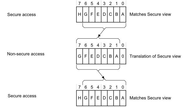
Image text
7 6 5 4 3 2 1 0
Secure access H G F E D C B A Matches Secure view
7 6 5 4 3 2 1 0
Non-secure access
G F E D C B A 0 Translation of Secure view
7 6 5 4 3 2 1 0
Secure access
H G F E D C B A Matches Secure view
Figure 4-9 shows how software reads of the interrupt priorities from Secure and Non-secure accesses relate to the priority values held in the Distributor, and to the interrupt values that are visible to Secure and Non-secure accesses. Figure 4-9 applies to a GIC that implements the maximum range of priority values.
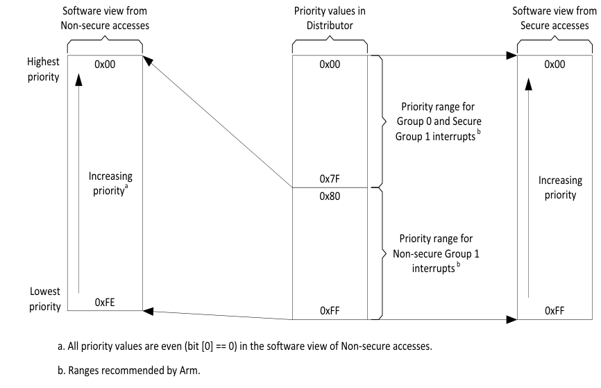
Image text
Software view from Priority values in Software view from
Non-secure accesses Distributor Secure accesses
Highest 0x00 0x00 0x00
priority
Priority range for
Group 0 and Secure
Group 1 interrupts [ b]
Increasing 0x7F Increasing
priority [a] 0x80 priority
Priority range for
Non-secure Group 1
interrupts [ b]
Lowest
0xFE
priority 0xFF 0xFF
a. All priority values are even (bit [0] == 0) in the software view of Non-secure accesses.
b. Ranges recommended by Arm.
Table 4-14 shows how the number of priority value bits implemented by the GIC affects the Secure and Non-secure reads of the priority of a Non-secure Group 1 interrupt.
Note Software executing in Non-secure state has no visibility of the priority settings of Group 0 interrupts, or where applicable, of Secure Group 1 interrupts.
Table 4-14 Effect of not implementing some priority field bits, two Security states
| Implemented priority bits, as seen by a Secure read [7:0] | Possible priority field values, for a Non-secure Group 1 interrupt Secure read Non-secure read | |—|— 0xFF-0x00(255-0), all values 0xFE-0x00(254-0), even values only | | [7:1] | 0xFE-0x00(254-0), even values only 0xFC-0x00(252-0), in steps of 4 | | [7:2] | 0xFC-0x00(252-0), in steps of 4 0xF8-0x00(248-0), in steps of 8 | | [7:3] | 0xF8-0x00(248-0), in steps of 8 0xF0-0x00(240-0), in steps of 16 |
This model for the presentation of priority values ensures software written to operate with an implementation of this GIC architecture functions as intended regardless of whether the GIC provides support for two Security states. However, programmers must ensure that software assigns the appropriate priority levels to the Group 0 and Group 1 interrupts.
Note To control priority values, Arm strongly recommends that:
- For a Group 0 interrupt, software sets bit[7] of the priority value field to 0.
- If using a Secure write to set the priority of a Non-secure Group 1 interrupt, software sets bit[7] of the priority value field to 1.
This ensures that all Group 0 and, if applicable, Secure Group 1 interrupts have higher priorities than all Non-secure Group 1 interrupts. However, a system might have requirements that cannot be met with this scheme.
Table 4-15 shows an example priority allocation scheme that ensures:
-
Some Group 0 interrupts have higher priority than any other interrupts.
-
Some Secure Group 1 interrupts have higher priority than any Non-secure Group 1 interrupt.
Table 4-15 Example priority allocation
| Interrupt security configuration | GICR_IPRIORITYR |
|---|---|
| Group 0 | 0b00 |
| Secure Group 1 | 0b01 |
| Non-secure Group 1 | 0b10 0b11 |
-
Software might not be aware that the GIC supports two Security states, and therefore might not know whether it is making Secure or Non-secure accesses to GIC registers. However, for any implemented interrupt, software can write 0xFF to the corresponding GICR_IPRIORITYR
priority value field, and then read back the value stored in the field to determine the supported interrupt priority range. Arm recommends that, before checking the priority range in this way: - For a peripheral interrupt, software first disables the interrupt.
-
For an SGI, software first checks that the interrupt is inactive.
4.8.7 Changing the priority of enabled PPIs, SGIs, and SPIs
If software writes to the GICD_IPRIORITYR
Chapter 5: Locality-specific Peripheral Interrupts and the ITS
This chapter describes Locality-specific Peripheral Interrupts (LPIs) and the Interrupt Translation Service (ITS). It contains the following sections:
-
LPIs.
-
The Interrupt Translation Service.
-
ITS commands.
-
Common ITS pseudocode functions.
-
ITS command error encodings.
-
ITS power management.
5.1 LPIs
Locality-specific Peripheral Interrupts (LPIs) are edge-triggered message-based interrupts that can use an Interrupt Translation Service (ITS), if it is implemented, to route an interrupt to a specific Redistributor and connected PE. GICv3 provides two types of support for LPIs. LPIs can be supported either:
-
Using the ITS to translate an EventID from a device into an LPI INTID. For more information about EventIDs, see The Interrupt Translation Service.
-
By forwarding an LPI INTID directly to the Redistributors, using GICR_SETLPIR.
An implementation must support only one of these methods.
Note
The following registers are mandatory in an implementation that supports LPIs but does not include an ITS:
-
GICR_INVLPIR.
-
GICR_INVALLR.
-
GICR_SYNCR.
Support for these registers is IMPLEMENTATION DEFINED in implementations that do include an ITS.
These registers control physical LPIs in a system that does not include an ITS:
-
GICR_SETLPIR.
-
GICR_CLRLPIR.
In an implementation that includes LPIs, at least 8192 LPIs are supported. For this reason, the configuration of each interrupt, and the pending information for each interrupt, is held in tables in memory, rather than in registers, and the tables are pointed to by registers held in the Redistributors.
Note
-
Arm expects that an implementation will cache parts of the tables in the Redistributors to reduce latency and memory traffic. The form of these caches is IMPLEMENTATION DEFINED.
-
The addresses for the LPI tables are in the Non-secure physical address space.
Figure 5-1 shows the generation of LPIs in an implementation that includes at least one ITS.
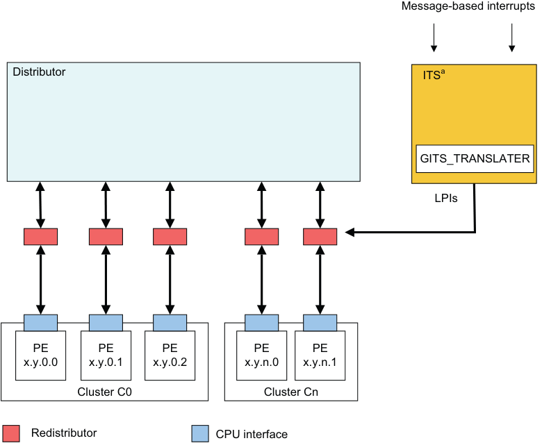
Image text
Message-based interrupts
Distributor ITS [a]
GITS_TRANSLATER
LPIs
PE PE PE PE PE
x.y.0.0 x.y.0.1 x.y.0.2 x.y.n.0 x.y.n.1
Cluster C0 Cluster Cn
Redistributor CPU interface
Figure 5-1 Triggering LPIs in an implementation with an ITS
Note In Figure 5-1, the ITS channel to the Redistributors is IMPLEMENTATION DEFINED.
Figure 5-2 shows the generation of LPIs in an implementation without an ITS. 5.1 LPIs
Message-based interrupts
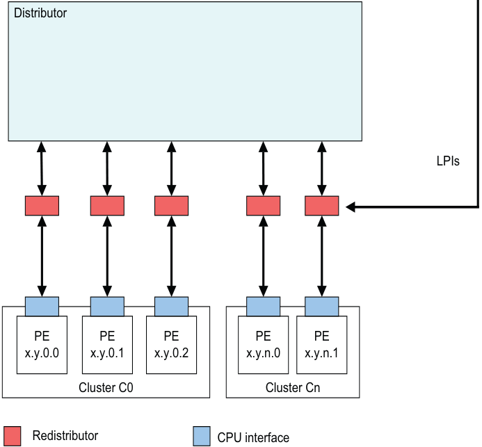
Image text
Distributor
LPIs
PE PE PE PE PE
x.y.0.0 x.y.0.1 x.y.0.2 x.y.n.0 x.y.n.1
Cluster C0 Cluster Cn
Redistributor CPU interface
-
LPIs are only supported when affinity routing is enabled for Non-secure state.
-
LPIs are always Non-secure Group 1 interrupts.
When GICD_CTLR.DS == 1:
-
LPIs are only supported when affinity routing is enabled.
-
LPIs are always Group 1 interrupts.
There is a single global physical LPI space so that LPIs can be moved between all Redistributors. Software programs the size of the single global physical LPI space using GICR_PROPBASER.IDbits.
Note The size of the physical LPI space is limited to the maximum size that an implementation supports, which is defined in GICD_TYPER.IDbits.
For a given Redistributor, LPI configuration and state are maintained in two tables in memory, described in the following sections:
-
LPI Configuration tables.
-
LPI Pending tables. If a Redistributor supports physical LPIs, it has:
-
LPI priority and enable bits programmed in the LPI Configuration table. The address of the LPI Configuration table is defined by GICR_PROPBASER. If GICR_PROPBASER is updated when GICR_CTLR.EnableLPIs == 1, the effects are UNPREDICTABLE. See LPI Configuration tables for more information.
-
Memory-backed storage for LPI pending bits in an LPI Pending table. This table is specific to a particular Redistributor. The address of the LPI Pending table is defined by GICR_PENDBASER. If GICR_PENDBASER is updated when GICR_CTLR.EnableLPIs == 1, the effects are UNPREDICTABLE.
GICR_PROPBASER.IDBits sets the size of the ID space, and thereby the number of entries in the LPI Configuration table and the corresponding LPI Pending table.
Physical LPIs are enabled by a write to GICR_CTLR.EnableLPIs.
Note
When LPIs are disabled at the Redistributor interface, that is when GICR_CTLR.EnableLPIs == 0, LPIs cannot become pending. An attempt to make an LPI pending in this situation has no effect, and the LPI is lost. This differs from disabling SGIs, PPIs, and SPIs, which prevents only the signaling of the interrupt to the CPU interface.
GICv4 introduces equivalent tables for handling virtual LPIs with addresses referenced in GICR_VPROPBASER and GICR_VPENDBASER.
In GICv4, virtual LPIs are enabled by a write to GICR_VPENDBASER.Valid.
5.1.1 LPI Configuration tables
LPI configuration is global. Whether a GIC supports Redistributors that point at different copies of the LPI Configuration table is IMPLEMENTATION DEFINED.
It is IMPLEMENTATION DEFINED whether GICR_PROPBASER can be set to different values on different Redistributors. GICR_TYPER.CommonLPIAff indicates which Redistributors must have GICR_PROPBASER set to the same value whenever GICR_CTLR.EnableLPIs == 1.
An implementation can treat all copies of GICR_PROPBASER that are required to have the same value as accessing common state.
Setting different values in different copies of GICR_PROPBASER on Redistributors that are required to use a common LPI Configuration table when GICR_CTLR.EnableLPIs == 1 leads to UNPREDICTABLE behavior.
If GICR_PROPBASER is programmed to different values on different Redistributors, it is IMPLEMENTATION DEFINED which copy or copies of GICR_PROPBASER are used when the GIC reads the LPI Configuration tables. However, the copy or copies that are used will correspond to a Redistributor on which GICR_CTLR.EnableLPIs == 1.
To avoid unpredictable behavior, software must ensure that all copies of the LPI Configuration tables are identical, and all changes are globally observable, whenever:
-
GICR_CTLR.EnableLPIs is written from 0 to 1 on any Redistributor.
-
GICR_INVLPIR and GICR_INVALLR are written on any Redistributor with GICR_CTLR.EnableLPIs == 1, if direct LPIs are supported.
-
The INV and INVALL command is executed by an ITS, in an implementation that includes at least one ITS.
An LPI Configuration table in memory stores entries containing configuration information for each LPI, where:
-
GICR_PROPBASER specifies a 4KB aligned physical address. This is the LPI Configuration table base address.
-
For any LPI N, the location of the table entry is defined by (base address + (N – 8192)).
To change the configuration of an interrupt, software writes to the LPI Configuration tables and then issues the INV or INVALL command. In implementations that do not include an ITS, software writes to GICR_INVALLR or GICR_INVLPIR. 5.1 LPIs
The LPI Configuration table contains an 8-bit entry for each LPI. Figure 5-3 shows the LPI Configuration table entry format.
7 2 1 0
Priority
RES1
Enable
Figure 5-3 LPI Configuration table entry
Table 5-1 shows the LPI Configuration table entry bit assignments.
Table 5-1 LPI Configuration table entry bit assignments
| Bits Name | Function |
|---|---|
| [7:2] Priority | The priority of the LPI. These are the most significant bits of the LPI priority. Bits[1:0] of the priority are 0. WhenGICD_CTLR.DS == 0, this value is shifted in accordance with the security and priority rules specified in_Software accesses of interrupt priority_on page 4-75. This means that LPI priorities are always in the lower half of the priority range. The priority value range is 128-254. IfGICD_CTLR.DS == 1, the value in this field is not shifted. In GICv4, the Virtual LPI Configuration tables behave as ifGICD_CTLR.DS == 1 and therefore the priority is not shifted. Note An implementation might support fewer than 8 bits of priority. Unimplemented bits will be treated asRES0. |
| See_Interrupt prioritization_on page 4-68for more information about interrupt priorities. | ||
|---|---|---|
| [1] | - | RES1. |
| [0] | Enable | LPI enable. This bit controls whether the LPI is enabled: 0 The LPI is not enabled. 1 The LPI is enabled. |
Caching
A Redistributor can cache the information from the LPI Configuration tables pointed to by GICR_PROPBASER, when GICR_CTLR.EnableLPI == 1, subject to all of the following rules:
-
Whether or not one or more caches are present is IMPLEMENTATION DEFINED. Where at least one cache is present, the structure and size is IMPLEMENTATION DEFINED.
-
An LPI Configuration table entry might be allocated into the cache at any time.
-
A cached LPI Configuration table entry is not guaranteed to remain in the cache.
-
A cached LPI Configuration table entry is not guaranteed to remain incoherent with memory.
-
A change to the LPI configuration is not guaranteed to be visible until an appropriate invalidation operation has completed:
- If one or more ITS is implemented, invalidation is performed using the INV or INVALL command. A SYNC command completes the INV and INVALL commands.
-
If no ITS is implemented, invalidation is performed by writing to GICR_INVALLR or GICR_INVLPIR.
If there is no Redistributor with GICR_CTLR.EnableLPIs == 1, the GIC has no cached LPI Configuration table entries.
5.1.2 LPI Pending tables
Software configures the LPI Pending tables, using the implemented range of valid LPI INTIDs, by writing to GICR_PENDBASER. This register provides the base address of the LPI Pending table for physical LPIs.
Each Redistributor maintains entries in a separate LPI Pending table that indicates the pending state of each LPI when GICR_CTLR.EnableLPIs == 1 in the Redistributor:
0 The LPI is not pending. 1 The LPI is pending.
For a given LPI:
-
The corresponding byte in the LPI Pending table is (base address + (N / 8)).
-
The bit position in the byte is (N MOD 8).
An LPI Pending table that contains only zeros, including in the first 1KB, indicates that there are no pending LPIs.
The first 1KB of the LPI Pending table is IMPLEMENTATION DEFINED. However, if the first 1KB of the LPI Pending table and the rest of the table contain only zeros, this must indicate that there are no pending LPIs.
The first 1KB of memory for the LPI Pending tables must contain only zeros on initial allocation, and this must be visible to the Redistributors, or else the effect is unpredictable.
During normal operation, the LPI Pending table is maintained solely by the Redistributor.
Behavior is UNPREDICTABLE if software writes to the LPI Pending tables while GICR_CTLR.EnableLPIs == 1. When GICR_CTLR.EnableLPIs is cleared to 0, behavior is UNPREDICTABLE if the LPI Pending table is written before GICR_CTLR.RWP reads 0.
Redistributors that are required to share a common LPI Configuration table, as indicated by GICR_TYPER.CommonLPIAff, might treat the OuterCache, Shareability, or InnerCache fields of GICR_PENDBASER as accessing common state.
Having the OuterCache, Shareability, or InnerCache fields of GICR_PENDBASER are programmed to different values on different Redistributors with GICR_CTLR.EnableLPIs == 1 in a system is unpredictable.
For physical LPIs, when GICR_CTLR.EnableLPIs is changed to 1, the Redistributor must read the pending status of the physical LPIs from the physical LPI Pending table.
Note
If GICR_PENDBASER.PTZ == 1, software guarantees that the LPI Pending table contains only zeros, including in the first 1KB. In this case hardware might not read any part of the table.
If GICR_CTLR.EnableLPIs is cleared to 0, then when GICR_CTLR.RWP reads as 0 there are no further accesses by the GIC to the LPI Pending table, and any caching of the LPI Pending table is invalidated. There is no guarantee that clearing GICR_CTLR.EnableLPIs causes the LPI Pending table to be updated in memory.
Note
If one or more ITS is implemented, Arm strongly recommends that all LPIs are mapped to another Redistributor before GICR_CTLR.EnableLPIs is cleared to 0.
For virtual LPIs, when GICR_CTLR.EnableLPIs ==1, and GICR_VPENDBASER.Valid is changed to 1, the Redistributor must read the pending status of the virtual LPIs from the virtual LPI Pending table.
Note
-
If GICR_VPENDBASER.IDAI == 0, the software guarantees that the LPI Pending table was written out by the same GIC implementation, meaning that hardware can rely on the first 1KB of the table and might not read the entire table.
-
If GICR_PROPBASER.IDbits is less than 0b1101 when GICR_CTLR.EnableLPIs == 1, the GIC might still access the IMPLEMENTATION DEFINED region of the LPI Pending table.
5.1.3 Virtual LPI Configuration tables and virtual LPI Pending tables
GICv4 uses the same concept of memory tables to hold the configuration and pending information for virtual LPIs. The format of these tables is the same as for physical LPIs.
5.2 The Interrupt Translation Service
The Interrupt Translation Service (ITS) translates an input EventID from a device, identified by its DeviceID, and determines:
-
The corresponding INTID for this input.
-
The target Redistributor and, through this, the target PE for that INTID.
For GICv3, the ITS performs this function for events that are translated into physical LPIs. LPIs can be forwarded to a Redistributor either by an ITS or by a direct write to GICR_SETLPIR. An implementation must support only one of these methods.
For GICv4, the ITS also performs this function for interrupts that are directly injected as virtual LPIs, and for GICV4.1, virtual SGIs.
An ITS has no effect on physical SGIs, SPIs, or PPIs.
The flow of the ITS translation is as follows:
-
The DeviceID selects a Device table entry (DTE) in the Device table that describes which Interrupt translation table (ITT) to use.
-
The EventID selects an Interrupt translation entry (ITE) in the ITT that describes:
-
For physical interrupts:
-
The output physical INTID.
-
The Interrupt collection number , ICID.
-
-
For virtual interrupts, in GICv4:
-
The output virtual INTID.
-
The vPEID.
-
A doorbell to use if the vPE is not scheduled.
-
-
-
For physical interrupts, ICID selects a Collection table entry in the Collection table (CT) that describes the target Redistributor, and therefore the target PE, to which the interrupt is routed.
-
For virtual interrupts, in GICv4, the vPEID selects a vPE table entry that describes the Redistributor that is currently hosting the target vPE to which the interrupt is routed.
The tables used in the translation process are described in more detail in the following sections:
-
The ITS tables .
-
The Device table.
-
The Interrupt translation table.
-
The Collection table.
-
The vPE table.
These tables are created and maintained using the ITS commands described in ITS commands. GICv3 and GICv4 do not support direct access to the tables, and the tables must be configured using the ITS commands.
5.2.1 The ITS tables
Software provisions memory for the ITS private tables when the GIC provides a set of registers that permits the following features to be discovered:
-
The number of private tables that are required.
-
The size of each entry in each table.
-
The type of each table.
Note
All ITS tables are in the Non-secure physical address space.
The state and configuration of the ITS tables is stored in a set of tables in memory. This memory is allocated by software before enabling the ITS.
GITS_BASER
The ITS tables have either a flat structure or a two-level structure. The structure is determined by GITS_BASER
-
0 Flat table. In this case a contiguous block of memory is allocated for the table. The format of the table is IMPLEMENTATION DEFINED.
- Behavior is UNPREDICTABLE if memory that is used for the ITS tables does not contain zeros at the time of the new allocation for use by the ITS.
-
1 Two-level table. In this case each entry in the level 1 table is 64 bits, and has the following format:
-
Bit[63] - Valid:
-
If this bit is cleared to 0, the PhysicalAddress field does not point to the base address of a level 2 table.
-
If this bit is set to 1, the PhysicalAddress field points to the base address of a level 2 table.
-
-
Bits[62:52] - RES 0.
-
Bits[51:N] - PhysicalAddress of the level 2 table. N is the number of bits that are required to specify the page size:
- The size of the level 2 table is determined by GITS_BASER
.Page_Size.
- The size of the level 2 table is determined by GITS_BASER
-
Bits[N-1:0] - RES 0. N is the number of bits that are required to specify the page size.
-
The level 1 table is indexed by the appropriate ID so that level 1 entry = ID/(Page Size / Entry Size).
-
Note This allows software to determine the level 2 table that must be allocated for a given CollectionID, DeviceID, or vPEID.
For level 1 table entries, when Valid == 0:
-
If the Type field specifies a valid table type other than a Collection table, the ITS discards any writes to the level 2 table.
-
If the Type field specifies the Collection table, and ICID is greater than or equal to the number indicated by GITS_TYPER.HCC, the ITS discards any writes to the level 2 table.
The format of the level 2 table is IMPLEMENTATION DEFINED.
Behavior is UNPREDICTABLE if:
-
Memory that is used for the level 2 tables does not contain zeros at the time of the new allocation for use by the ITS.
-
Multiple level 1 table entries with Valid == 1 point to the same level 2 table.
Note As part of restoring the state of the ITS from powerdown events, the registers that describe the table can point to tables that were previously populated by the ITS, and so might contain values other than zeros. The details of power management of the ITS are IMPLEMENTATION DEFINED. See ITS power management.
Figure 5-4 shows how these tables are used in the translation process.
Image text
Device
table
Interrupt Redistributor A
Source
vPE table
(GICv4 only) Virtual
pending table
Interrupt
translation
table
Redistributor B
Collection
table Pending table
pINTID (direct LPI support)
DeviceID
vPEID
CollectionID
vINTID
EventID
pINTID
When GITS_CTLR.Enabled is written from 0 to 1 behavior is UNPREDICTABLE if any of the following conditions are true:
-
GITS_CBASER.Valid == 0.
-
GITS_BASER
.Valid == 0, for any GITS_BASER register where the Type field indicates Device. -
GITS_BASER
.Valid == 0, for any GITS_BASER register where the Type field indicates collection and GITS_TYPER.HCC == 0. -
In GICv4, GITS_BASER
.Valid == 0, for any GITS_BASER register where the Type field indicates a vPE.
Software access to the private ITS tables.
If GITS_BASER
If GITS_BASER
When GITS_CTLR.Enabled == 0 and GITS_CTLR.Quiescent == 1:
- An implementation will not access the tables that are pointed to by any of the GITS_BASER
registers.
When GITS_CTLR.Enabled == 1 or GITS_CTLR.Quiescent == 0:
-
An implementation will not access a table that is pointed to by any GITS_BASER
register for which GITS_BASER .Valid == 0. -
For a table that is pointed to by a GITS_BASER
register for which GITS_BASER .Valid == 1 and GITS_BASER .Indirect == 0, behavior is UNPREDICTABLE if the table is written by software. -
For a table that is pointed to by a GITS_BASER
register for which GITS_BASER .Valid == 1 and GITS_BASER .Indirect == 1: -
Behavior is UNPREDICTABLE if any of the level 2 table entries are written by software.
-
An ITS will not cache any entry in the level 1 table where the valid bit is cleared to 0.
-
-
Behavior is UNPREDICTABLE if any level 1 table entry where the valid bit set to 1 is written by software.
-
A write to a level 1 table entry that changes the valid bit from 0 to 1 must be globally visible before software adds a command to the ITS command queue that relies on that entry. Otherwise it is UNKNOWN if the command will succeed or if it will be ignored.
5.2.2 Interrupt collections
In GICv3, the ITS considers all physical LPIs that it generates to be members of collections . The data that is associated with a collection can be held in the ITS, in external memory, or in both. The ITS supports collections that are held in memory if any of the GITS_BASER
-
When the ITS supports collections that are held in memory, the total number of collections that is supported is determined by the memory allocated by software:
-
If GITS_BASER
.Indirect == 0, the number of collections supported in memory can be calculated using the following formula:
((number of pages * page size) / entry size) The relevant values for this formula are indicated in GITS_BASER
- If GITS_BASER
.Indirect == 1, the number of collections supported in memory can be calculated using the following formula:
(((number of pages in level 1 table * page size) /8) * (page size/entry size)). The relevant values for this formula are indicated in GITS_BASER
Note
Indirect tables allow sparse allocations, so not all ICIDs in the supported range might be usable.
- Where collections are held in both the ITS and external memory, the total number of collections is indicated by GITS_TYPER.CCT.
When GITS_TYPER.HCC!= 0:
-
Collections with identifiers in the range {0… GITS_TYPER.HCC-1} are held in the ITS.
-
Collections with identifiers in the range greater than that indicated in GITS_TYPER.HCC are held in external memory, if this is supported.
When GITS_TYPER.HCC == 0:
- The ITS must support collections in external memory, and all collections are held in external memory.
The maximum number of collections that are supported is limited by the size of the ICID:
-
If GITS_TYPER.CIL == 0, the ICID is 16 bits.
-
If GITS_TYPER.CIL == 1, the ICID is reported by GITS_TYPER.CIDbits.
5.2.3 The Device table
The Device table provides a table of Device table entries (DTEs). Each DTE describes a mapping between a DeviceID and an ITT base address that points to the memory that the ITS can use to store the translations for the EventID. The ITS uses the ITT to store the translations for every EventID for the specified DeviceID. The DeviceID is a unique identifier assigned to each device that can create a range of EventIDs. For example, Arm expects that the 16-bit Requester ID from a PCIe Root Complex is presented to an ITS as a DeviceID.
The DeviceID provides the index value for the table. Table 5-2 shows an example of the number of bits that might be assigned to each DTE.
Table 5-2 DTE entries
| Number of bits | Assignment | Notes |
|---|---|---|
| 1 | Valid | Boolean |
| 40 | ITT Address | Base physical address |
| 5 | ITT Range | Log2 (EventID width supported by the ITT) minus one. |
5.2.4 The Interrupt translation table
An Interrupt translation table (ITT) is specific to each device that can create numbered events. Each entry in an ITT is referred to as an Interrupt translation entries (ITEs).
In GICv3, ITEs are only defined for physical interrupts.
In GICv4, ITEs are defined for physical interrupts and for virtual interrupts, and provide a distinction between:
-
An entry for a physical LPI and the use of an ICT for routing information.
-
An entry for a virtual LPI and the use of a vPE table .
An ITT must be assigned a contiguous physical address space starting at ITT Address. The size is 2^(DTE.ITT Range + 1)* GITS_TYPER.ITT_entry_size.
Behavior is UNPREDICTABLE if the memory does not contain all zeros at the time of new allocation for use by the ITS.
If multiple ITTs overlap in memory, behavior is UNPREDICTABLE.
ITS accesses to an ITT use the same Shareability and Cacheability attributes that are specified for the Device table.
For physical interrupts, each ITE describes the mapping between the input EventID and:
-
The output physical INTID (pINTID) that is sent to the target PE.
-
The ICID that identifies an entry in the Collection table, that determines the target PE for the LPI. For more information about the Collection table, see The Collection table.
For virtual interrupts, each ITE describes the mapping of the EventID as outlined in the preceding list, and:
-
The output virtual INTID (vINTID) that is sent to the target vPE.
-
The virtual PE number (vPEID) that identifies an entry in the vPE table to determine the current host Redistributor. For more information about the vPE table, see The vPE table.
-
A physical LPI that is sent to a physical PE if a virtual interrupt is translated when the target vPE is not currently scheduled on a physical PE.
The EventID provides the index value for the table.
Table 5-3 shows an example of the number of bits that might be stored in an ITE.
Table 5-3 ITE entries
| Number of bits | Assignment | Notes |
|---|---|---|
| 1 | Valid | Boolean |
| 1 | Interrupt_Type | Boolean, indicates whether the interrupt is physical or virtual. |
| Size of the LPI number spacea | Interrupt_Number | pINTID or vINTID depending on the interrupt type. |
| Table 5-3 ITE entries (continued) |
| Number of bits | Assignment | Notes |
|---|---|---|
| Size of the LPI | Interrupt_Number | In GICv4 pINTID is used as a doorbell. In GICv3, and in |
| number spacea | HypervisorID | GICv4 when a doorbell is not required, the programmed value is 1023. |
| 16 | ICID | Interrupt Collection ID, for physical interrupts only. |
| 16 | vPEID | vPE ID, for virtual interrupt only. |
a. For information about the size of the LPI number space, see INTIDs.
5.2.5 The Collection table
The Collection table (CT) provides a table of Collection table entries (CTEs). For physical LPIs only, each CTE describes a mapping between:
-
The ICID generated by the ITT.
-
The address of the target Redistributor in the format defined by GITS_TYPER.PTA.
There is a single CT for each ITS, which can be held in registers or in memory, or in a combination of the two. See GITS_BASER
The TableID provides the index value for the table. It is derived from ICID.
Table 5-4 shows an example of the number of bits that might be assigned to each CT.
Table 5-4 CT entries
| Number of bits | Assignment | Notes |
|---|---|---|
| 1 | Valid | Boolean |
| Size of RDbase identifier | RDbase | The GIC supports two formats for RDbase, seeRDbase |
5.2.6 The vPE table
The vPE table consists of vPE table entries that provide a mapping from the vPEID generated by the ITS to:
-
The target Redistributor, in the format defined by GITS_TYPER.PTA.
-
The base address of the virtual LPI Pending table associated with the target vPE.
An area of memory defined by GITS_BASER
The vPE table describes all the vPEs associated with an ITS. Table 5-5 shows an example of the number of bits that an implementation might store in a vPE table. The 16-bit vPEID provides the index value for the table.
Table 5-5 vPE table entries
| Number of bits | Assignment | Notes |
|---|---|---|
| 1 | Valid | Boolean |
| Size of RDbase identifier | RDbase | The GIC supports two formats forRDbase. |
| Size of | VPT_addr | VPT_addr locates the LPI Pending table when the VM is not |
| address | resident in the Redistributor. It is used as the address in GICR_VPENDBASERwhen the vPE is scheduled in the GICR_* registers associated with RDbase. | |
| 5 | Size | The size of the vINTID range supported (minus one). |
5.2.7 Control and configuration of the ITS
An ITS is controlled and configured using a memory-mapped interface where:
-
The version can be read from GITS_IIDR and from GITS_PIDR2.
-
GITS_TYPER specifies the features that are supported by an ITS.
-
GITS_CTLR controls the operation of an ITS.
-
GITS_TRANSLATER receives EventID information. It is IMPLEMENTATION DEFINED how the DeviceID is supplied. See ITS commands for more details.
-
GITS_BASER
registers provide information about the type, size and access attributes for the architected ITS memory structures. -
GITS_CBASER, GITS_CREADR, and GITS_CWRITER store address information for the ITS command queue interface.
There is an enable bit for each ITS, GITS_CTLR.Enabled.
5.2.8 The ITS command interface
Figure 5-5 shows how the ITS provides the base address and the size that are used by the ITS command queue.
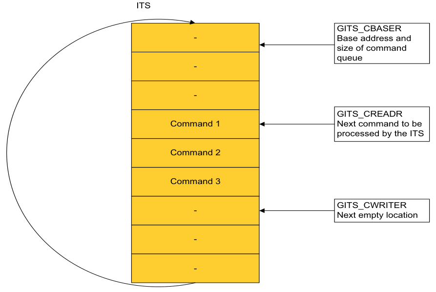
Image text
ITS
GITS_CBASER
- Base address and
size of command
queue
-
-
GITS_CREADR
Command 1 Next command to be
processed by the ITS
Command 2
Command 3
- GITS_CWRITERNext empty location
-
-
GITS_CBASER, GITS_CREADR, and GITS_CWRITER define the ITS command queue.
-
GITS_CBASER uses the following fields:
-
Valid. This field indicates the allocation of memory for the ITS command queue.
-
Cacheability. This field indicates the cacheability attributes of accesses to the ITS command queue.
-
Shareability. This field indicates the Shareability attributes of accesses to the ITS command queue.
-
Physical address. This field provides the base physical address of the memory containing the ITS command queue.
-
Size. This field indicates the number of 4KB pages of physical memory for the ITS command queue.
-
-
GITS_CREADR specifies the base address offset from which an ITS reads the next command to execute.
-
GITS_CWRITER specifies the base address offset of the next free entry to which software writes the next command.
The size of an ITS command queue entry is 32 bytes. This means that there is support for 128 entries in each 4KB page.
The ITS command queue uses a little endian memory order model.
In the ITS command queue:
-
The base address is always aligned to 64KB.
-
Size is expressed as a multiple of 4KB.
-
The address at which the queue wraps is always aligned to 4KB, and is (base address + (Size * 4KB)).
Note
All addresses are Non-secure physical addresses. When the first command is complete, the ITS starts to process the next command. The read pointer, GITS_CREADR, advances as the ITS processes commands. If GITS_CREADR reaches the top of the memory specified in GITS_CBASER then the pointer wraps back to the base address specified in GITS_CBASER. GITS_CWRITER is controlled by software.
The ITS command queue is empty when GITS_CWRITER and GITS_CREADR specify the same base address offset value.
The ITS command queue is full when GITS_CWRITER points to an address 32 bytes behind GITS_CREADR in the buffer.
When GITS_CREADR.Stalled == 1 no subsequent commands are processed.
The INT ITS command generates an interrupt on execution, and this can generate an interrupt on completion of a particular sequence of commands, see ITS commands.
5.2.9 Ordering of translations with the output to ITS commands
Each command queue entry appears to be executed atomically so that a translation request either sees the state of the ITS before a command or the state of the ITS after the command.
A translation request initiated after a SYNC or VSYNC command has completed is translated using an ITS state that is consistent with the state after the command is performed.
In the absence of a SYNC or VSYNC command the ordering of ITS commands and translation requests is not defined by the architecture.
5.2.10 Restrictions for INTID mapping rules
The behavior of the GIC is unpredictable if software:
-
Maps multiple EventID-DeviceID combinations to the same physical LPI INTID.
-
Assigns doorbell interrupts with the same physical LPI INTID to different physical PEs. This applies to GICv4 only.
-
Maps an EventID-DeviceID combination and an individual doorbell interrupt to the same physical LPI INTID, unless they target the same physical PE. This applies to all versions of GICv4.
-
Maps multiple EventID-DeviceID combinations to the same virtual LPI INTID-vPEID. This applies to GICv4 only.
-
Maps an EventID-DeviceID combination and a default doorbell interrupt to the same physical LPI INTID. This applies to GICv4.1 only.
-
Maps a default doorbell and an individual doorbell to the same physical LPI INTID. This applies to GICv4.1 only.
Note Conceptually the restriction is that software should not map multiple EventID-DeviceID combinations to the same vLPI within a given virtual machine. However, the ITS has no awareness of which vPEs belong to the same virtual machine.
5.3 ITS commands
Table 5-6 provides a summary of all ITS commands.
Table 5-6 ITS commands
| Command Command arguments | Description |
|---|---|
| CLEAR DeviceID, EventID | Translates the event defined byEventID and DeviceIDinto anICIDand pINTID, and instruct the appropriate Redistributor to remove the pending state. |
| DISCARD DeviceID, EventID | Translates the event defined byEventID and DeviceIDand instructs the appropriate Redistributor to remove the pending state of the interrupt. It also ensures that any caching in the Redistributors associated with a specificEventIDis consistent with the configuration held in memory. DISCARDremoves the mapping of theDeviceIDandEventIDfrom the ITT, and ensures that incoming requests with a particularEventIDare silently discarded. |
| INT DeviceID, EventID | Translates the event defined byEventID and DeviceIDinto anICIDand pINTID, and instruct the appropriate Redistributor to set the interrupt pending. |
| INV DeviceID, EventID | Specifies that the ITS must ensure that any caching in the Redistributors associated with the specifiedEventIDis consistent with the LPI Configuration tables held in memory. |
| INVALL ICID | Specifies that the ITS must ensure any caching associated with the interrupt collection defined byICIDis consistent with the LPI Configuration tables held in memory for all Redistributors. |
| INVDB GICv4.1 only vPEID | GICv4.1 only. Specifies that the ITS must ensure any caching associated with the default doorbell forvPEIDis consistent with the LPI Configuration tables held in memory for all Redistributors. |
| MAPC ICID, RDbase | Maps the Collection table entry defined byICIDto the target Redistributor, defined byRDbase. |
| MAPD DeviceID, ITT_addr, Size | Maps the Device table entry associated withDeviceIDto its associated ITT, defined byITT_addrandSize. |
| MAPI DeviceID, EventID, ICID | Maps the event defined byEventID and DeviceIDinto an ITT entry with ICIDandpINTID=EventID. Note • pINTID≥0x2000for a valid LPI INTID. • This is equivalent toMAPTI DeviceID, EventID, EventID, ICID |
| MAPTIa DeviceID, EventID, pINTID, ICID | Maps the event defined byEventIDandDeviceIDto its associated ITE, defined byICIDandpINTIDin the ITT associated withDeviceID. Note pINTID≥0x2000for a valid LPI INTID. Note pINTID≥0x2000 |
| MOVALL RDbase1, RDbase2 | Instructs the Redistributor specified byRDbase1to move all of its interrupts to the Redistributor specified byRDbase2. |
| Table 5-6 ITS commands (continued) |
| Command Command arguments | Description |
|---|---|
| MOVI DeviceID, EventID, ICID | Updates theICIDfield in the ITT entry for the event defined byDeviceID andEventID. It also translates the event defined byEventIDandDeviceID into anICIDandpINTID, and instructs the appropriate Redistributor to move the pending state, if it is set, of the interrupt to the Redistributor defined by the newICID, and to update the ITE associated with the event to use the newICID. |
| SYNC RDbase | Ensures all outstanding ITS operations associated with physical interrupts for the Redistributor specified byRDbaseare globally observed before any further ITS commands are executed. Following the execution of a SYNC the effects of all previous commands must apply to subsequent writes toGITS_TRANSLATER. See_Ordering of_ _translations with the output to ITS commands_on page 5-97for more information. |
| VINVALLb vPEID | Ensures any cached Redistributor information associated withvPEIDis consistent with the associated LPI Configuration tables held in memory. |
| VMAPIb DeviceID, EventID, Dbell_pINTID, vPEID | Maps the event defined byDeviceIDandEventIDinto an ITT entry with vPEID,vINTID=EventID, andDbell_PINTID, a doorbell provision. Note • vINTID≥0x2000for a valid LPI INTID. • This is equivalent toVMAPTI DeviceID, EventID, EventID, pINTID, vPEID • Dbell_pINTIDmust be either 1023 orDbell_pINTID≥0x2000for a valid LPI INTID. |
| VMAPP GICv4.0b vPEID, RDbase, VPT_addr, VPT_size | Maps the vPE table entry defined byvPEIDto the targetRDbase, including an associated virtual LPI Pending table (VPT_addr, VPT_size). |
| VMAPP GICv4.1 vPEID, RDbase, VCONF_addr, VPT_addr, VPT_size, PTZ, Alloc, Default_Doorbell_pINTID | Maps the vPE defined byvPEID, including the associated virtual LPI Configuration and Pending tables. Optionally, specifying a default doorbell. |
| VMAPTIbc DeviceID, EventID, vINTID, Dbell_pINTID, vPEID | Maps the event defined byDeviceIDandEventIDinto an ITT entry with vPEIDandvINTID, andDbell_pINTID, a doorbell provision. Note • vINTID≥0x2000for a valid LPI INTID. • Dbell_pINTIDmust be either 1023 orDbell_pINTID≥0x2000for a valid LPI INTID. |
| VMOVIb DeviceID, EventID, vPEID | Updates thevPEIDfield in the ITT entry for the event defined byDeviceID andEventID. Translates the event defined byEventIDandDeviceIDinto a vPEIDandpINTID, and instructs the appropriate Redistributor to move the pending state, if it is set, of the interrupt to the Redistributor defined by the newvPEID, and updates the ITE associated with the event to use the newvPEID. |
| VMOVP GICv4.0b vPEID, RDbase, SequenceNumber, ITSList | Updates the vPE table entry defined byvPEIDto the target Redistributor specified byRDbase. Software must useSequenceNumberandITSListto synchronize the execution of VMOVP commands across more than one ITS. |
Arm IHI 0069G Table 5-6 ITS commands (continued)
| Command | Command arguments | Description |
|---|---|---|
| VMOVP | vPEID, RDbase, SequenceNumber, | Update the vPE mapping defined forvPEIDto the target Redistributor |
| GICv4.1 | ITSList, Default_Doorbell_pINTID | defined by RDbase. |
| VSGI for | vPEID, Priority, G, C, E, vPEID | GICv4.1 only. For the vPE defined byvPEID, sets the configuration or |
| GICv4.1 onlyb | updates the state of the interrupt defined by vINTID. | |
| VSYNCb | vPEID | Ensures all outstanding ITS operations for thevPEIDspecified are globally observed before any further ITS commands are executed. Following the execution of a VSYNC the effects of all previous commands must apply to subsequent writes to GITS_TRANSLATER. |
-
a. This command was previously called MAPVI.
-
b. This command exists in GICv4 only.
-
c. This command was previously called VMAPVI.
The number of bits of EventID and DeviceID that an implementation supports are discoverable from GITS_TYPER. Unimplemented bits are RES0.
Note
-
The INTID of an LPI is in the range of 8192 - maximum number. The maximum number is IMPLEMENTATION DEFINED. See INTIDs.
-
The following argument names have been changed from those used in preliminary information associated with this GIC specification:
-
Device has been changed to DeviceID.
-
ID has been changed to EventID.
-
pID has been changed to pINTID.
-
vID has been changed to vINTID.
-
pCID has been changed to ICID.
-
target address has been changed to RDbase.
-
VCPU has been changed to vPE.
-
-
The format of the collection target address, RDbase, is indicated by GITS_TYPER.PTA.
5.3.1 IMPLEMENTATION DEFINED sizes in ITS command parameters
Some ITS commands include the following types of parameter that have an IMPLEMENTATION DEFINED size:
DeviceIDs
The maximum number of Device identifiers supported by the associated Device table is determined by the number of bits available, as specified by GITS_TYPER.Devbits.
EventID EventID is limited by the maximum MAPD Size field, which is limited by GITS_TYPER.ID_bits. ICID The number of collections supported is IMPLEMENTATION DEFINED:
• For implementations that do not support Collection tables in external memory, GITS_TYPER.HCC indicates the number of collections.
• For implementations that do support Collection tables in external memory, the number of supported collections is limited by the size of the allocated collection table: — The total number of collections supported is calculated as follows: GITS_TYPER.HCC + (Size of collection table / Entry size) When GITS_TYPER.CIL == 1, the maximum number of collections is limited by GITS_TYPER.CIDbits. pINTID pINTID is limited by GICR_PROPBASER.IDbits, which is limited by GICD_TYPER.IDbits. This also applies to Dbell_pINTID.
RDbase
RDbase is associated with a Redistributor and is specified in one of two formats:
- The base physical address of RD_base when GITS_TYPER.PTA == 1.
Note Addresses can be up to 52 bits in size and must be 64KB aligned. The RDbase field consists of bits[51:16] of the address.
-
A PE number, as indicated in GICR_TYPER.Processor_Number when GITS_TYPER.PTA == 0.
-
vINTID vINTID can be limited by GICR_VPROPBASER.IDbits, which is limited by GICD_TYPER.IDbits.
vPEID vPEID is limited by the size of the vPE table.
5.3.2 Command errors
If the ITS detects an error in the data provided to a command, the resulting behavior is a CONSTRAINED UNPREDICTABLE choice of:
-
Ignoring the command:
-
No action is performed that alters the handling of interrupts.
-
GITS_CREADR is incremented to point to the next command, wrapping if necessary.
-
If GITS_TYPER.SEIS is set to 1, a System error is generated.
-
Note
It is IMPLEMENTATION DEFINED how the System error is recorded and how it is reported to the PE.
-
Stalling the ITS command queue:
-
GITS_CREADR is not incremented and continues to point to the entry that triggered the error.
-
— GITS_CREADR.Stalled is set to 1.
-
Software can restart the processing of commands by writing 1 to GITS_CWRITER.Retry.
-
If GITS_TYPER.SEIS is set to 1, a System error is generated.
- Note
-
It is IMPLEMENTATION DEFINED how the system error is recorded and how it is reported to the PE.
-
Treating the data as valid data:
-
The data that generated the error or errors is treated as having a legal value, and the command is processed accordingly.
-
GITS_CREADR is incremented to point to the next command, wrapping if necessary.
-
If GITS_TYPER.SEIS is set to 1 a System error is generated.
-
Note
It is IMPLEMENTATION DEFINED how the System error is recorded and how it is reported to the PE.
See ITS command error encodings for more information.
5.3.3 CLEAR
This command translates the event defined by EventID and DeviceID into an ICID and pINTID, and instructs the appropriate Redistributor to remove the pending state.
Figure 5-6 shows the format of the CLEAR command.
| 63 | 32 | 31 | 8 | 7 0 | 7 0 | DW | |||
|---|---|---|---|---|---|---|---|---|---|
| DeviceID | RES0 | 0x04 | 0 | ||||||
| RES0 | EventID | 1 | |||||||
| RES0 | 2 | ||||||||
| RES0 | 3 |
Figure 5-6 CLEAR command format
In Figure 5-6:
-
EventID identifies the interrupt, associated with a device, for which the pending state is to be cleared.
-
DeviceID specifies the requesting device.
-
DW is the doubleword offset within a 32 byte, or four doubleword, ITS command packet.
The command and its arguments are:
CLEAR DeviceID, EventID
A command error occurs if any of the following apply:
-
DeviceID exceeds the maximum value supported by the ITS.
-
The device specified by DeviceID is not mapped to an Interrupt translation table, using MAPD.
-
EventID exceeds the maximum value allowed by the ITT. This value is specified by the Size field when the MAPD command is issued.
-
The EventID for the device is not mapped to a collection, using MAPI or MAPTI.
-
The EventID for the device is mapped to a collection that has not been mapped to an RDbase using MAPC.
In this case, the ITS must take the actions described in Command errors.
The following pseudocode describes the operation of the CLEAR command:
// ITS.CLEAR // =========
ITS.CLEAR(ITSCommand cmd)
    if DeviceOutOfRange(cmd.DeviceID)
    then if GITS_TYPER.SEIS == '1'
    then IMPLEMENTATION_DEFINED "SError CLEAR_DEVICE_OOR";
UNPREDICTABLE;
dte = ReadDeviceTable(UInt(cmd.DeviceID));
if !dte.Valid then
    if GITS_TYPER.SEIS == '1' then
        IMPLEMENTATION_DEFINED "SError CLEAR_UNMAPPED_DEVICE";
        UNPREDICTABLE;
    if IdOutOfRange(cmd.EventID, dte.ITT_size) then
        if GITS_TYPER.SEIS == '1' then
            IMPLEMENTATION_DEFINED "SError CLEAR_ID_OOR";
            UNPREDICTABLE;
        InterruptTableEntry ite = ReadTranslationTable(dte.ITT_base, UInt(cmd.EventID));
        if !ite.Valid then
            if GITS_TYPER.SEIS == '1' then
                IMPLEMENTATION_DEFINED "SError CLEAR_UNMAPPED_INTERRUPT";
                UNPREDICTABLE;
            success = ClearPendingState(ite);
            if !success then
                if GITS_TYPER.SEIS == '1' then
                    IMPLEMENTATION_DEFINED "SError CLEAR_ITE_INVALID";
                    UNPREDICTABLE;
                IncrementReadPointer();
                return;
5.3.4 DISCARD
This command translates the event defined by EventID and DeviceID and instructs the appropriate Redistributor to remove the pending state of the interrupt. It also ensures that any caching in the Redistributors associated with a specific EventID is consistent with the configuration held in memory. DISCARD removes the mapping of the DeviceID and EventID from the ITT, and ensures that incoming requests with a particular EventID are silently discarded.
Figure 5-7 shows the format of the DISCARD command.
| 63 | 32 | 31 | 8 | 7 0 | DW | |||
|---|---|---|---|---|---|---|---|---|
| DeviceID | RES0 | 0x0F | 0 | |||||
| RES0 | EventID | 1 | ||||||
| RES0 | 2 | |||||||
| RES0 | 3 |
Figure 5-7 DISCARD command format
In Figure 5-7:
-
EventID identifies the interrupt, associated with a device, that is to be discarded.
-
DeviceID specifies the requesting device.
-
DW is the doubleword offset within a 32 byte, or four doubleword, ITS command packet.
The command and its arguments are:
DISCARD DeviceID, EventID
A command error occurs if any of the following apply:
-
DeviceID exceeds the maximum value supported by the ITS.
-
The device specified by DeviceID is not mapped to an ITT, using MAPD.
-
EventID exceeds the maximum value allowed by the ITT. This value is specified by the Size field when the MAPD command is issued.
-
The EventID for the device is not mapped to a collection, using MAPI or MAPTI.
-
The EventID for the device is mapped to a collection that has not been mapped to an RDbase using MAPC.
In this case, the ITS must take the actions described in Command errors.
In GICv4.1, when this command is issued for an EventID and DeviceID that maps to a virtual LPI, and the associated vPEID is not mapped to a Redistributor on that ITS:
-
It removes the mapping for the EventID and DeviceID on the ITS.
-
If the vPE is mapped on at least one other ITS, it is IMPLEMENTATION DEFINED whether the pending state is cleared.
-
If the vPE is not mapped on any ITS, the pending state is not cleared.
A vPEID is classed as not mapped if no VMAPP with V=1 has been issued for it, or if it has been unmapped by a VMAPP with V=0.
The following pseudocode describes the operation of the DISCARD command:
// ITS.DISCARD // ===========
ITS.DISCARD(ITSCommand cmd)
    if DeviceOutOfRange(cmd.DeviceID)
    then if GITS_TYPER.SEIS == '1'
    then IMPLEMENTATION_DEFINED "SError DISCARD_DEVICE_OOR";
UNPREDICTABLE;
DeviceTableEntry dte = ReadDeviceTable(UInt(cmd.DeviceID));
if !dte.Valid then
    if GITS_TYPER.SEIS == '1' then
        IMPLEMENTATION_DEFINED "SError DISCARD_UNMAPPED_DEVICE";
        UNPREDICTABLE;
    if IdOutOfRange(cmd.EventID, dte.ITT_size) then
        if GITS_TYPER.SEIS == '1' then
            IMPLEMENTATION_DEFINED "SError DISCARD_ID_OOR";
            UNPREDICTABLE;
        InterruptTableEntry ite = ReadTranslationTable(dte.ITT_base, UInt(cmd.EventID));
        if ite.Valid then success = ClearPendingState(ite);
        if !success then
            if GITS_TYPER.SEIS == '1' then
                IMPLEMENTATION_DEFINED "SError DISCARD_ITE_INVALID";
                UNPREDICTABLE;
        else if GITS_TYPER.SEIS == '1' then
            IMPLEMENTATION_DEFINED "SError DISCARD_UNMAPPED_INTERRUPT";
            UNPREDICTABLE;
ite.Valid = FALSE; WriteTranslationTable(dte.ITT_base, UInt(cmd.EventID), ite);
IncrementReadPointer(); return;
5.3.5 INT
This command translates the event defined by EventID and DeviceID into an ICID and pINTID, and instructs the appropriate Redistributor to set the interrupt pending.
Figure 5-8 shows the format of the INT command.
| 63 | 32 | 31 | 8 | 7 0 | DW | |||
|---|---|---|---|---|---|---|---|---|
| DeviceID | RES0 | 0x03 | 0 | |||||
| RES0 | EventID | 1 | ||||||
| RES0 | 2 | |||||||
| RES0 | 3 |
Figure 5-8 INT command format In Figure 5-8:
-
EventID identifies an interrupt source associated with a device. The ITS then translates this into an LPI INTID.
-
DeviceID specifies the requesting device.
-
DW is the doubleword offset within a 32 byte, or four doubleword, ITS command packet.
The command and its arguments are:
INT DeviceID, EventID
A command error occurs if any of the following apply:
-
DeviceID exceeds the maximum value supported by the ITS.
-
The device specified by DeviceID is not mapped to an ITT, using MAPD.
-
EventID exceeds the maximum value allowed by the ITT. This value is specified by the Size field when the MAPD command is issued.
-
EventID is not mapped to a collection, using MAPI or MAPTI.
-
The EventID for the device is mapped to a collection that has not been mapped to an RDbase using MAPC.
In this case, the ITS must take the actions described in Command errors.
The following pseudocode describes the operation of the INT command:
// ITS.INT // ======= ITS.INT(ITSCommand cmd)
if DeviceOutOfRange(cmd.DeviceID) then
    if GITS_TYPER.SEIS == '1' then
        IMPLEMENTATION_DEFINED "SError INT_DEVICE_OOR";
        UNPREDICTABLE;
    DeviceTableEntry dte = ReadDeviceTable(UInt(cmd.DeviceID));
    if !dte.Valid then
        if GITS_TYPER.SEIS == '1' then
            IMPLEMENTATION_DEFINED "SError INT_UNMAPPED_DEVICE";
            UNPREDICTABLE;
        if IdOutOfRange(cmd.EventID, dte.ITT_size) then
            if GITS_TYPER.SEIS == '1' then
                IMPLEMENTATION_DEFINED "SError INT_ID_OOR";
                UNPREDICTABLE;
            InterruptTableEntry ite = ReadTranslationTable(dte.ITT_base, UInt(cmd.EventID));
            if !ite.Valid then
                if GITS_TYPER.SEIS == '1' then
                    IMPLEMENTATION_DEFINED "SError INT_UNMAPPED_INTERRUPT";
                    UNPREDICTABLE;
                boolean success = SetPendingState(ite);
                if !success then
                    if GITS_TYPER.SEIS == '1' then
                        IMPLEMENTATION_DEFINED "SError INT_ITE_INVALID";
                        UNPREDICTABLE;
                    IncrementReadPointer();
                    return;
5.3.6 INV
This command specifies that the ITS must ensure that any caching in the Redistributors associated with the specified EventID is consistent with the LPI Configuration tables held in memory.
In GICv4.1, it is IMPLEMENTATION DEFINED whether INV affects the generation and prioritization of default doorbells.
Note The INV command performs the same function regardless of whether the interrupt is mapped as a physical interrupt or a virtual interrupt.
Figure 5-9 shows the format of the INV command.
| 63 | 32 | 31 | 8 | 7 0 | DW | |||
|---|---|---|---|---|---|---|---|---|
| DeviceID | RES0 | 0x0C | 0 | |||||
| RES0 | EventID | 1 | ||||||
| RES0 | 2 | |||||||
| RES0 | 3 |
Figure 5-9 INV command format
In Figure 5-9:
-
EventID identifies an interrupt source associated with a device. The ITS then translates this into an LPI INTID.
-
DeviceID specifies the requesting device.
-
DW is the doubleword offset within a 32 byte, or four doubleword, ITS command packet. The command and its arguments are:
INV DeviceID, EventID
A command error occurs if any of the following apply:
-
DeviceID exceeds the maximum value supported by the ITS.
-
The device specified by DeviceID is not mapped to an ITT, using MAPD.
-
EventID exceeds the maximum value allowed by the ITT. This value is specified by the Size field when the MAPD command is issued.
-
EventID is not mapped to a collection, using MAPI or MAPTI.
-
The EventID for the device corresponds to a physical LPI and is mapped to a collection that has not been mapped to an RDbase using MAPC.
-
The EventID for the device corresponds to a virtual LPI associated with a vPE that has not been mapped to a Redistributor using VMAPP GICv4.0 or VMAPP GICv4.1.
In this case, the ITS must take the actions described in Command errors.
The following pseudocode describes the operation of the INV command:
// ITS.INV // ======= ITS.INV(ITSCommand cmd)
if DeviceOutOfRange(cmd.DeviceID) then
    if GITS_TYPER.SEIS == '1' then
        IMPLEMENTATION_DEFINED "SError INV_DEVICE_OOR";
        UNPREDICTABLE;
    DeviceTableEntry dte = ReadDeviceTable(UInt(cmd.DeviceID));
    if !dte.Valid then
        if GITS_TYPER.SEIS == '1' then
            IMPLEMENTATION_DEFINED "SError INV_UNMAPPED_DEVICE";
            UNPREDICTABLE;
        if IdOutOfRange(cmd.EventID, dte.ITT_size) then
            if GITS_TYPER.SEIS == '1' then
                IMPLEMENTATION_DEFINED "SError INV_ID_OOR";
                UNPREDICTABLE;
            InterruptTableEntry ite = ReadTranslationTable(dte.ITT_base, UInt(cmd.EventID));
            if !ite.Valid then
                if GITS_TYPER.SEIS == '1' then
                    IMPLEMENTATION_DEFINED "SError INV_UNMAPPED_INTERRUPT";
                    UNPREDICTABLE;
                invalidateByITE(ite);
                IncrementReadPointer();
                return;
5.3.7 INVALL
This command specifies that the ITS must ensure any caching associated with the interrupt collection defined by ICID is consistent with the LPI Configuration tables held in memory for all Redistributors.
In GICv4.1, it is IMPLEMENTATION DEFINED whether INVALL affects the generation and prioritization of default doorbells.
Figure 5-10 shows the format of the INVALL command.
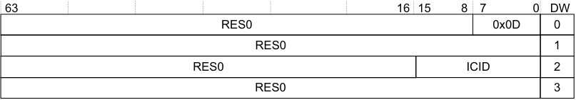
Image text
63 16 15 8 7 0 DW
RES0 0x0D 0
RES0 1
RES0 ICID 2
RES0 3
In Figure 5-10:
-
ICID specifies the interrupt collection.
-
DW is the doubleword offset within a 32 byte, or four doubleword, ITS command packet.
The command and its arguments are:
INVALL ICID
A command error occurs if any of the following apply:
-
The collection specified by ICID exceeds the maximum number supported by the ITS.
-
The collection specified by ICID has not been mapped to an RDbase using MAPC.
In this case, the ITS must take the actions described in Command errors.
The following pseudocode describes the operation of the INVALL command:
// ITS.INVALL // ==========
ITS.INVALL(ITSCommand cmd)
    if (CollectionOutOfRange(cmd.ICID))
    then if GITS_TYPER.SEIS == '1'
    then IMPLEMENTATION_DEFINED "SError INVALL_COLLECTION_OOR";
UNPREDICTABLE;
CollectionTableEntry cte = ReadCollectionTable(UInt(cmd.ICID));
if !cte.Valid then
    if GITS_TYPER.SEIS == '1' then
        IMPLEMENTATION_DEFINED "SError INVALL_UNMAPPED_COLLECTION";
        UNPREDICTABLE;
    // This invalidates any caches containing the configuration data
    for all interrupts in the
    // collection. Over invalidation is permitted.
    InvalidateCollectionCaches(UInt(cmd.ICID));
    IncrementReadPointer();
    return;
5.3.8 INVDB GICv4.1 only
In GICv4.1, the ITS command INVDB is allocated to invalidate the configuration of default doorbells:
Figure 5-11 shows the format of the INVDB command for GICv4.1 only.
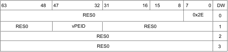
Image text
63 48 47 32 31 16 15 8 7 0 DW
RES0 0x2E 0
RES0 vPEID RES0 1
RES0 2
RES0 3
- vPEID = The vPEID of the vPE.
// ITS.INVDB // ========= ITS.INVDB(ITSCommand cmd)
if VCPUOutOfRange(cmd.VCPUID) then
    if GITS_TYPER.SEIS == 1 then
        IMPLEMENTATION_DEFINED "SError INVDB_VCPU_OOR";
        UNPREDICTABLE;
    VCPUTableEntry vte = ReadVCPUTable(UInt(cmd.VCPUID));
    if vte.Valid then InvalidateInterruptDoorbellCaches(VCPUID, vte);
    IncrementReadPointer();
    return;
INVDB is synchronized by a VSYNC command.
After completion of an INVDB command, there is no caching associated with the default doorbell of the specified vPE in any Redistributor.
A command error occurs if any of the following apply:
- An INVDB is issued with a vPEID that exceeds the configured maximum vPEID for the ITS: INVDB_VCPU_OOR (0x01_2E11).
An INVDB with a valid vPEID behaves as a NOP if either of the following points is true:
-
The vPEID is not mapped on the ITS.
-
The vPEID has no default doorbell.
5.3.9 MAPC
This command maps the Collection table entry defined by ICID to the target Redistributor, defined by RDbase.
Figure 5-12 shows the format of the MAPC command.
| 63 | 62 | 51 | 50 | 16 | 8 15 | 7 0 | DW | |||
|---|---|---|---|---|---|---|---|---|---|---|
| RES0 | 0x09 | 0 | ||||||||
| RES0 | 1 | |||||||||
| V | RES0 | RDbase | ICID | 2 | ||||||
| RES0 | 3 |
Figure 5-12 MAPC command format
In Figure 5-12:
-
V specifies whether RDbase is valid for the collection.
-
RDbase specifies the target Redistributor to which interrupts in the collection are forwarded. See IMPLEMENTATION DEFINED sizes in ITS command parameters.
-
ICID specifies the interrupt collection that is to be mapped.
-
DW is the doubleword offset within a 32 byte, or four doubleword, ITS command packet.
If GITS_TYPER.PTA == 1 and a physical address is specified, the target addresses must be 64KB aligned, meaning that only bits[47:16] are required. See IMPLEMENTATION DEFINED sizes in ITS command parameters for more information. In addition, when V is cleared to 0, this field must be written as zero, but hardware might ignore the value.
The command and its arguments are: MAPC ICID, RDbase, V
When V is 1:
-
Behavior is unpredictable if there are interrupts that are mapped to the specified collection and the collection is currently mapped to a Redistributor, unless MAPC is followed by MOVALL so that the pending state for the collection is moved from the old target Redistributor or the new target Redistributor. MOVALL might be issued by a different ITS:
-
Where multiple collections are remapped from the same source to the same destination, behavior is unpredictable if MOVALL is issued before all the MAPCs are globally observable.
-
Behavior is unpredictable if any ITS command that affects interrupts that belong to a remapped collection is issued after the MAPC, but before the MOVALL is globally observable.
-
-
Behavior is unpredictable if RDbase does not specify a valid Redistributor.
When V is 0:
-
MAPC removes the mapping of the specified interrupt collection. Interrupts for that are mapped to this collection are ignored.
-
Behavior is unpredictable if there are interrupts that are mapped to the specified collection, with the restriction that further translation requests from that device are ignored.
A command error occurs if the following applies:
- The collection specified by ICID exceeds the maximum number supported by the ITS.
In this case, the ITS must take the actions described in Command errors.
Note
When software uses a MAPC command to move a collection from targeting Redistributor A to targeting Redistributor B, it must issue a SYNC command to Redistributor A before issuing the accompanying MOVALL command. Otherwise, interrupts from the collection might still be taken by the PE associated with Redistributor A.
The following pseudocode describes the operation of the MAPC command:
// ITS.MAPC // ======== ITS.MAPC(ITSCommand cmd)
if CollectionOutOfRange(cmd.ICID) then
    if GITS_TYPER.SEIS == '1' then
        IMPLEMENTATION_DEFINED "SError MAPC_COLLECTION_OOR";
        UNPREDICTABLE;
    CollectionTableEntry cte;
    cte.Valid  = cmd.V == '1';
    cte.RDbase = cmd.RDbase;
    WriteCollectionTable(UInt(cmd.ICID), cte);
    IncrementReadPointer();
    return;
5.3.10 MAPD
This command maps the Device table entry associated with DeviceID to its associated ITT, defined by ITT_addr and Size.
Figure 5-13 shows the format of the MAPD command.
| 63 | 62 | 52 | 51 | 32 | 31 | 8 | 7 5 | 0 4 | DW | ||
|---|---|---|---|---|---|---|---|---|---|---|---|
| DeviceID | RES0 | 0x08 | 0 | ||||||||
| RES0 | Size | 1 | |||||||||
| V | RES0 | ITT_addr | RES0 | 2 | |||||||
| RES0 | 3 |
Figure 5-13 MAPD command format In Figure 5-13:
- DeviceID specifies the device that uses the ITT.
Note For more information about mapping devices to ITTs, see The Interrupt translation table.
-
V specifies whether the ITT_addr and Size fields are valid.
-
ITT_addr specifies bits[51:8] of the physical address of the ITT.
-
Size is a 5-bit number that specifies the supported number of bits for the device, minus one. The size field enables range checking of EventID for translation requests for this DeviceID.
-
DW is the doubleword offset within a 32 byte, or four doubleword, ITS command packet.
Behavior is UNPREDICTABLE if any of the following apply:
-
There is an existing mapping for the DeviceID and the mapped ITT contains valid EventID mappings.
-
When V == 1, the specified ITT does not contain all zeros.
The command and its arguments are:
MAPD DeviceID, ITT_addr, Size, V
The format of the ITT entries is IMPLEMENTATION DEFINED. A typical example entry size of 8 bytes permits allocation of identifiers to devices in multiples of 32 interrupts.
When V is 1:
-
MAPD associates a DeviceID with a 256 byte-aligned address of an ITT.
-
When V is 0:
-
MAPD removes the mapping for the specified DeviceID. Translation requests from that device are ignored.
-
MAPD removes the mapping of the specified DeviceID. and interrupt requests from that device are discarded. A subsequent translation for the DeviceID does not generate and LPI or VLPI until DeviceID has been mapped to the ITT again.
A command error occurs if any of the following apply:
-
DeviceID exceeds the maximum number of devices supported by an ITS.
-
Size exceeds the maximum value permitted by the settings of GITS_TYPER.ID_bits, when V is set to 1.
In this case, the ITS must take the actions described in Command errors.
Note ITS accesses to an ITT use the same Shareability and Cacheability attributes that are specified for the Device table, see The Device table.
The following pseudocode describes the operation of the MAPD command:
// ITS.MAPD // ======== ITS.MAPD(ITSCommand cmd)
    if DeviceOutOfRange(cmd.DeviceID)
    then if GITS_TYPER.SEIS == '1'
    then IMPLEMENTATION_DEFINED "SError MAPD_DEVICE_OOR";
UNPREDICTABLE;
if SizeOutOfRange(cmd.Size) then

if GITS_TYPER.SEIS == '1' then IMPLEMENTATION_DEFINED "SError MAPD_ITTSIZE_OOR"; UNPREDICTABLE;
// If a device is Re-mapped software must perform the following actions
// to ensure the LPI configuration is up to date:
// 1. Ensure that the device is quiescent and that all interrupts have
//     been handled.
// 2. Remap the device with the new (empty) ITT
//
DeviceTableEntry dte;
5.3.11 MAPI
This command maps the event defined by EventID and DeviceID into an ITT entry with ICID and pINTID = EventID.
Note
-
pINTID ≥0x2000 for a valid LPI INTID.
-
This is equivalent to MAPTI DeviceID, EventID, EventID, ICID
Figure 5-14 shows the format of the MAPI command.
| 63 | 32 | 31 | 16 | 8 15 | 7 0 | DW | ||
|---|---|---|---|---|---|---|---|---|
| DeviceID | RES0 | 0x0B | 0 | |||||
| RES0 | EventID | 1 | ||||||
| RES0 | ICID | 2 | ||||||
| RES0 | 3 |
Figure 5-14 MAPI command format
In Figure 5-14:
-
EventID identifies the interrupt, associated with a device, that is to be mapped.
-
DeviceID specifies the requesting device.
-
ICID specifies the interrupt collection that includes the specified interrupt.
-
DW is the doubleword offset within a 32 byte, or four doubleword, ITS command packet.
If there is an existing mapping for the EventID-DeviceID combination, behavior is UNPREDICTABLE.
The command and its arguments are:
MAPI DeviceID, EventID, ICID
A command error occurs if any of the following apply:
-
DeviceID exceeds the maximum value supported by the ITS.
-
The device specified by DeviceID is not mapped to an ITT, using MAPD.
-
ICID exceeds the maximum number of interrupt collections supported by an ITS. For more information, see The Collection table.
-
The EventID exceeds the maximum value allowed by the ITT. This value is specified by the Size field when the MAPD command is issued. • EventID does not specify a valid LPI identifier. See INTIDs. In this case, the ITS must take the actions described in Command errors. The following pseudocode describes the operation of the MAPI command:
// ITS.MAPI // ======== ITS.MAPI(ITSCommand cmd)
if DeviceOutOfRange(cmd.DeviceID) then
    if GITS_TYPER.SEIS == '1' then
        IMPLEMENTATION_DEFINED "SError MAPI_DEVICE_OOR";
        UNPREDICTABLE;
    if CollectionOutOfRange(cmd.ICID) then
        if GITS_TYPER.SEIS == '1' then
            IMPLEMENTATION_DEFINED "SError MAPI_COLLECTION_OOR";
            UNPREDICTABLE;
        DeviceTableEntry dte = ReadDeviceTable(UInt(cmd.DeviceID));
        if !dte.Valid then
            if GITS_TYPER.SEIS == '1' then
                IMPLEMENTATION_DEFINED "SError MAPI_UNMAPPED_DEVICE";
                UNPREDICTABLE;
            if IdOutOfRange(cmd.EventID, dte.ITT_size) then
                if GITS_TYPER.SEIS == '1' then
                    IMPLEMENTATION_DEFINED "SError MAPI_ID_OOR";
                    UNPREDICTABLE;
                if LPIOutOfRange(cmd.EventID) then
                    if GITS_TYPER.SEIS == '1' then
                        IMPLEMENTATION_DEFINED "SError MAPI_ID_OOR";
                        UNPREDICTABLE;
                    InterruptTableEntry ite = ReadTranslationTable(dte.ITT_base, UInt(cmd.EventID));
ite.Valid = TRUE; ite.Type = physical_interrupt; ite.OutputID = cmd.EventID; ite.DoorbellID = ZeroExtend(INTID_SPURIOUS); // Don’t generate a doorbell ite.ICID = cmd.ICID;
WriteTranslationTable(dte.ITT_base, UInt(cmd.EventID), ite);
IncrementReadPointer();
return;
5.3.12 MAPTI
This command maps the event defined by EventID and DeviceID to its associated ITE, defined by ICID and pINTID in the ITT associated with DeviceID.
Figure 5-15 shows the format of the MAPTI command.
| 63 | 32 | 31 | 16 | 8 15 | 7 0 | DW | ||
|---|---|---|---|---|---|---|---|---|
| DeviceID | RES0 | 0x0A | 0 | |||||
| pINTID | EventID | 1 | ||||||
| RES0 | ICID | 2 | ||||||
| RES0 | 3 |
Figure 5-15 MAPTI command format In Figure 5-15:
-
EventID identifies the interrupt, associated with a device, that is to be mapped.
-
pINTID is the INTID of the physical interrupt that is presented to software.
-
DeviceID specifies the requesting device.
-
ICID specifies the interrupt collection that includes the specified physical interrupt.
-
DW is the doubleword offset within a 32 byte, or four doubleword, ITS command packet.
If there is an existing mapping for the EventID-DeviceID combination, behavior is UNPREDICTABLE.
The command and its arguments are:
MAPTI DeviceID, EventID, pINTID, ICID
A command error occurs if any of the following apply:
-
DeviceID exceeds the maximum value supported by the ITS.
-
The device specified by DeviceID is not mapped to an ITT using MAPD.
-
The number of collections exceeds the maximum number of collections supported by the ITS. For more information, see The Collection table.
-
The EventID exceeds the maximum value allowed by the ITT. This value is specified by the Size field when the MAPD command is issued.
-
pINTID does not specify a valid LPI INTID. For information about the LPI INTID range, see INTIDs.
In this case, the ITS must take the actions described in Command errors.
The following pseudocode describes the operation of the MAPTI command:
// ITS.MAPTI // =========
ITS.MAPTI(ITSCommand cmd)
if DeviceOutOfRange(cmd.DeviceID) then
    if GITS_TYPER.SEIS == '1' then
        IMPLEMENTATION_DEFINED "SError MAPTI_DEVICE_OOR";
        UNPREDICTABLE;
    if CollectionOutOfRange(cmd.ICID) then
        if GITS_TYPER.SEIS == '1' then
            IMPLEMENTATION_DEFINED "SError MAPTI_COLLECTION_OOR";
            UNPREDICTABLE;
        DeviceTableEntry dte = ReadDeviceTable(UInt(cmd.DeviceID));
        if !dte.Valid then
            if GITS_TYPER.SEIS == '1' then
                IMPLEMENTATION_DEFINED "SError MAPTI_UNMAPPED_DEVICE";
                UNPREDICTABLE;
            if IdOutOfRange(cmd.EventID, dte.ITT_size) then
                if GITS_TYPER.SEIS == '1' then
                    IMPLEMENTATION_DEFINED "SError MAPTI_ID_OOR";
                    UNPREDICTABLE;
                if LPIOutOfRange(cmd.pINTID) then
                    if GITS_TYPER.SEIS == '1' then
                        IMPLEMENTATION_DEFINED "SError MAPTI_PHYSICALID_OOR";
                        UNPREDICTABLE;
                    InterruptTableEntry ite = ReadTranslationTable(dte.ITT_base, UInt(cmd.EventID));
ite.Valid = TRUE; ite.Type = physical_interrupt; ite.OutputID = cmd.pINTID; ite.DoorbellID = ZeroExtend(INTID_SPURIOUS); // Don’t generate a doorbell ite.ICID = cmd.ICID;
WriteTranslationTable(dte.ITT_base, UInt(cmd.EventID), ite);
IncrementReadPointer();
return;
5.3.13 MOVALL
This command instructs the Redistributor specified by RDbase1 to move all of its interrupts to the Redistributor specified by RDbase2.
Note Both the mapping of interrupts to collections and the mapping of collections to Redistributors are normally unaffected by this command. Software must ensure that any interrupts that might be affected by this command target the Redistributor specified by RDbase2, otherwise system behavior is UNPREDICTABLE. In particular, an implementation might choose to remap all affected collections to RDbase2.
Figure 5-16 shows the format of the MOVALL command.
| 63 | 51 | 50 | 32 | 31 | 16 | 8 15 | 7 0 | DW | |
|---|---|---|---|---|---|---|---|---|---|
| RES0 | 0x0E | 0 | |||||||
| RES0 | 1 | ||||||||
| RES0 | Rdbase 1 | RES0 | 2 | ||||||
| RES0 | Rdbase 2 | RES0 | 3 |
Figure 5-16 MOVALL command format
In Figure 5-16:
-
RDbase1 specifies the Redistributor with which the interrupts are currently associated. See IMPLEMENTATION DEFINED sizes in ITS command parameters.
-
RDbase2 specifies the Redistributor to which the interrupts are to be moved. See IMPLEMENTATION DEFINED sizes in ITS command parameters.
-
DW is the doubleword offset within a 32 byte, or four doubleword, ITS command packet.
The command and its arguments are:
MOVALL RDbase1, RDbase2
Behavior is unpredictable if RDbase1 and RDbase2 do not specify a valid Redistributor. The format of these fields is specified by GITS_TYPER.PTA.
MOVALL targeting a RD with LPIs disabled is CONSTRAINED UNPREDICTABLE, with a choice of:
-
Clear the pending state of all moved LPIs.
-
Act as NOP, with the pending state is unchanged on the source RD.
The following pseudocode describes the operation of the MOVALL command:
// ITS.MOVALL // ==========
ITS.MOVALL(ITSCommand cmd) rd1 = cmd.RD1base;
rd2 = cmd.RD2base;
if rd1 != rd2
    then MoveAllPendingState(rd1, rd2);
IncrementReadPointer();
return;
5.3.14 MOVI
This command updates the ICID field in the ITT entry for the event defined by DeviceID and EventID. It also translates the event defined by EventID and DeviceID into an ICID and pINTID, and instructs the appropriate Redistributor to move the pending state, if it is set, of the interrupt to the Redistributor defined by the new ICID, and to update the ITE associated with the event to use the new ICID.
Figure 5-17 shows the format of the MOVI command.
| 63 | 32 | 31 | 16 | 8 15 | 7 0 | DW | ||
|---|---|---|---|---|---|---|---|---|
| DeviceID | RES0 | 0x01 | 0 | |||||
| RES0 | EventID | 1 | ||||||
| RES0 | ICID | 2 | ||||||
| RES0 | 3 |
Figure 5-17 MOVI command format
In Figure 5-17:
-
EventID identifies the interrupt, associated with a device, that is to be redirected.
-
DeviceID specifies the requesting device.
-
ICID specifies the new interrupt collection that is to include the specified physical interrupt.
-
DW is the doubleword offset within a 32 byte, or four doubleword, ITS command packet.
The command and its arguments are:
MOVI DeviceID, EventID, ICID
A command error occurs if any of the following apply:
-
DeviceID exceeds the maximum value supported by the ITS.
-
The device specified by DeviceID is not mapped to an ITT, using MAPD.
-
ICID exceeds the maximum number of interrupt collections supported by an ITS.
-
ICID is not mapped to an RDbase using MAPC.
-
EventID is not mapped to a collection, using MAPI or MAPTI.
-
EventID corresponds to a virtual LPI.
In this case, the ITS must take the actions described in Command errors.
Note If, after using MOVI to move an interrupt from collection A to collection B, software moves the same interrupt again from collection B to collection C, a SYNC command must be used before the second MOVI for the Redistributor associated with collection A to ensure correct behavior.
When MOVI is issued targeting a Collection that is unmapped, or mapped to a Redistributor with LPIs disabled, behavior is CONSTRAINED UNPREDICTABLE, with a choice of:
-
Clear the pending state of the moved LPI.
-
Pending state unchanged on the source RD.
The following pseudocode describes the operation of the MOVI command:
// ITS.MOVI // ========
ITS.MOVI(ITSCommand cmd)
if DeviceOutOfRange(cmd.DeviceID) then
    if GITS_TYPER.SEIS == '1' then
        IMPLEMENTATION_DEFINED "SError MOVI_DEVICE_OOR";
        UNPREDICTABLE;
    if CollectionOutOfRange(cmd.ICID) then
        if GITS_TYPER.SEIS == '1' then
            IMPLEMENTATION_DEFINED "SError MOVI_COLLECTION_OOR";
            UNPREDICTABLE;
        DeviceTableEntry dte = ReadDeviceTable(UInt(cmd.DeviceID));
        if !dte.Valid then
            if GITS_TYPER.SEIS == '1' then
                IMPLEMENTATION_DEFINED "SError MOVI_UNMAPPED_DEVICE";
                UNPREDICTABLE;
            if IdOutOfRange(cmd.EventID, dte.ITT_size) then
                if GITS_TYPER.SEIS == '1' then
                    IMPLEMENTATION_DEFINED "SError MOVI_ID_OOR";
                    UNPREDICTABLE;
                InterruptTableEntry ite = ReadTranslationTable(dte.ITT_base, UInt(cmd.EventID));
                if !ite.Valid then
                    if GITS_TYPER.SEIS == '1' then
                        IMPLEMENTATION_DEFINED "SError MOVI_UNMAPPED_INTERRUPT";
                        IncrementReadPointer();
                        return;
                    if ite.Type == virtual_interrupt then
                        if GITS_TYPER.SEIS == '1' then
                            IMPLEMENTATION_DEFINED "SError MOVI_ID_IS_VIRTUAL";
                            UNPREDICTABLE;
                        CollectionTableEntry cte1 = ReadCollectionTable(UInt(ite.ICID));
                        if !cte1.Valid then
                            if GITS_TYPER.SEIS == '1' then
                                IMPLEMENTATION_DEFINED "SError MOVI_UNMAPPED_COLLECTION";
                                UNPREDICTABLE;
                            CollectionTableEntry cte2 = ReadCollectionTable(UInt(cmd.ICID));
                            if !cte2.Valid then
                                if GITS_TYPER.SEIS == '1' then
                                    IMPLEMENTATION_DEFINED "SError MOVI_UNMAPPED_COLLECTION";
                                    IncrementReadPointer();
                                    return;
                                bits(32) rd1 = cte1.RDbase;
                                bits(32) rd2 = cte2.RDbase;
                                if rd1 != rd2 then
                                    // Move the move the pending state to rd2
                                    if set taking care of any races where the
                                    // interrupt has been forwarded to the processor
                                    MovePendingState(rd1, rd2, ite.OutputID);
5.3.15 SYNC
This command ensures all outstanding ITS operations associated with physical interrupts for the Redistributor specified by RDbase are globally observed before any further ITS commands are executed. Following the execution of a SYNC, the effects of all previous commands must apply to subsequent writes to GITS_TRANSLATER.
Figure 5-18 shows the format of the SYNC command.
| 63 | 51 | 50 | 32 | 31 | 16 | 8 15 | 7 0 | DW | |
|---|---|---|---|---|---|---|---|---|---|
| RES0 | 0x05 | 0 | |||||||
| RES0 | 1 | ||||||||
| RES0 | RDbase | RES0 | 2 | ||||||
| RES0 | 3 |
Figure 5-18 SYNC command format In Figure 5-18:
-
RDbase specifies the physical address of the target Redistributor. The format of the target address is determined by GITS_TYPER.PTA. See IMPLEMENTATION DEFINED sizes in ITS command parameters for more information.
-
DW is the doubleword offset within a 32 byte, or four doubleword, ITS command packet.
The command and its arguments are:
SYNC RDbase
The following pseudocode describes the operation of the SYNC command:
// Wait for the external effects of any virtual commands to be observable by all redistributors
// and ensure the internal effects of any previous commands affect any subsequent interrupt
// requests or commands
WaitForVirtualCompletion(rd_base);

IncrementReadPointer();

return;
5.3.16 VINVALL
This command ensures that any cached Redistributor information associated with vPEID is consistent with the associated LPI Configuration tables held in memory.
This command is provided only in GICv4.
Figure 5-19 shows the format of the VINVALL command.
| 63 | 48 | 47 | 32 | 31 | 8 | 7 0 | DW | |
|---|---|---|---|---|---|---|---|---|
| RES0 | 0x2D | 0 | ||||||
| RES0 | vPEID | RES0 | 1 | |||||
| RES0 | 2 | |||||||
| RES0 | 3 |
Figure 5-19 VINVALL command format
In Figure 5-19:
-
vPEID specifies the vPE.
-
DW is the doubleword offset within a 32 byte, or four doubleword, ITS command packet.
The command and its arguments are:
VINVALL vPEID
A command error occurs if any of the following apply:
-
vPEID exceeds the maximum number supported by the ITS, as defined by GITS_BASER
. -
The PE specified by vPEID is not mapped to a Redistributor using VMAPP GICv4.0.
In this case, the ITS must take the actions described in Command errors. The following pseudocode describes the operation of the VINVALL command:
// ITS.VINVALL // ===========
ITS.VINVALL(ITSCommand cmd)
    if VCPUOutOfRange(cmd.VCPUID) then
if GITS_TYPER.SEIS == '1' then
    IMPLEMENTATION_DEFINED "SError VINVALL_VCPU_OOR";
    UNPREDICTABLE;
VCPUTableEntry vte = ReadVCPUTable(UInt(cmd.VCPUID));
if !vte.Valid then
    if GITS_TYPER.SEIS == '1' then
        IMPLEMENTATION_DEFINED "SError VINVALL_VCPU_INVALID";
        UNPREDICTABLE;
    InvalidateVCPUCaches(UInt(cmd.VCPUID));
    IncrementReadPointer();
    return;
5.3.17 VMAPI
This command maps the event defined by DeviceID and EventID into an ITT entry with vPEID, vINTID=EventID, and Dbell_PINTID, a doorbell provision.
Note
-
vINTID ≥0x2000 for a valid LPI INTID.
-
This is equivalent to VMAPTI DeviceID, EventID, EventID, pINTID, vPEID.
-
Dbell_pINTID must be either 1023 or Dbell_pINTID ≥0x2000 for a valid LPI INTID.
This command is provided only in GICv4.
Figure 5-20 shows the format of the VMAPI command.
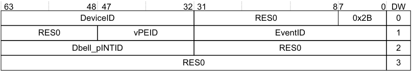
Image text
63 48 47 32 31 8 7 0 DW
DeviceID RES0 0x2B 0
RES0 vPEID EventID 1
Dbell_pINTID RES0 2
RES0 3
In Figure 5-20:
-
EventID identifies the interrupt, associated with a device, that is to be presented to the VM.
-
DeviceID specifies the requesting device.
-
vPEID specifies the vPE.
-
Dbell_pINTID specifies the ID that is presented to the hypervisor if the vPE is not scheduled.
- Note
If Dbell_pINTID indicates a spurious interrupt, then no physical interrupt is generated.
- DW is the doubleword offset within a 32 byte, or four doubleword, ITS command packet.
If there is an existing mapping for the EventID-DeviceID combination, behavior is UNPREDICTABLE.
The command and its arguments are:
VMAPI DeviceID, EventID, Dbell_pINTID, vPEID A command error occurs if any of the following apply:
-
DeviceID exceeds the maximum value supported by the ITS.
-
vPEID exceeds the maximum number supported by the ITS, as defined by GITS_BASER
. -
The device specified by DeviceID is not mapped to an ITT, using MAPD.
-
EventID exceeds the maximum value allowed by the ITT. This value is specified by the Size field when the MAPD command is issued.
-
EventID does not specify a valid LPI INTID. For information about valid LPI INTIDs, see INTIDs.
-
Dbell_pINTID does not specify a valid doorbell INTID, where a valid INTID is either: — 1023.
- Within the supported range for LPIs.
In this case, the ITS must take the actions described in Command errors.
The following pseudocode describes the operation of the VMAPI command:
// ITS.VMAPI // =========
ITS.VMAPI(ITSCommand cmd)
    if DeviceOutOfRange(cmd.DeviceID)
    then if GITS_TYPER.SEIS == '1'
    then IMPLEMENTATION_DEFINED "SError VMAPI_DEVICE_OOR";
UNPREDICTABLE;
if VCPUOutOfRange(cmd.VCPUID) then
    if GITS_TYPER.SEIS == '1' then
        IMPLEMENTATION_DEFINED "SError VMAPI_VCPU_OOR";
        UNPREDICTABLE;
    DeviceTableEntry dte = ReadDeviceTable(UInt(cmd.DeviceID));
    if !dte.Valid then
        if GITS_TYPER.SEIS == '1' then
            IMPLEMENTATION_DEFINED "SError VMAPI_UNMAPPED_DEVICE";
            UNPREDICTABLE;
        if IdOutOfRange(cmd.EventID, dte.ITT_size) then
            if GITS_TYPER.SEIS == '1' then
                IMPLEMENTATION_DEFINED "SError VMAPI_ID_OOR";
                UNPREDICTABLE;
            if LPIOutOfRange(cmd.EventID) then
                if GITS_TYPER.SEIS == '1' then
                    IMPLEMENTATION_DEFINED "SError VMAPI_ID_OOR";
                    UNPREDICTABLE;
                if LPIOutOfRange(cmd.Dbell_pINTID) then
                    if GITS_TYPER.SEIS == '1' then
                        IMPLEMENTATION_DEFINED "SError VMAPI_PHYSICALID_OOR";
                        UNPREDICTABLE;
                    InterruptTableEntry ite = ReadTranslationTable(dte.ITT_base, UInt(cmd.EventID));
ite.Valid = TRUE; ite.Type = virtual_interrupt; ite.OutputID = cmd.EventID; ite.DoorbellID = cmd.Dbell_pINTID; ite.VCPUID = cmd.VCPUID;
WriteTranslationTable(dte.ITT_base, UInt(cmd.EventID), ite);
IncrementReadPointer();
return;
5.3.18 VMAPP GICv4.0
This command maps the vPE table entry defined by vPEID to the target RDbase, including an associated virtual LPI Pending table (VPT_addr, VPT_size).
Figure 5-21 shows the format of the VMAPP command for GICv4.0.
| 63 | 62 | 51 | 50 | 32 | 31 | 16 | 8 15 | 7 5 | 0 4 | DW | |
|---|---|---|---|---|---|---|---|---|---|---|---|
| RES0 | 0x29 | 0 | |||||||||
| RES0 | vPEID | RES0 | 1 | ||||||||
| V | RES0 | RDbase | RES0 | 2 | |||||||
| RES0 | VPT_addr | RES0 | VPT_ size | 3 |
Figure 5-21 VMAPP GICv4.0 command format In Figure 5-21:
-
vPEID specifies the vPE.
-
V specifies whether the RDbase and VPT_addr are valid for the vPE.
-
RDbase specifies the target Redistributor that owns the vPE and to which the ITS directs commands for that PE. See IMPLEMENTATION DEFINED sizes in ITS command parameters.
-
VPT_addr specifies bits [51:16] of the physical address of the virtual LPI Pending table for the vPE.
Note The target addresses must be 64KB aligned, meaning that only bits [51:16] are required. Bits [15:0] of the physical address are 0.
-
VPT_size specifies the number of vINTID bits that the vPE supports, minus one.
-
DW is the doubleword offset within a 32 byte, or four doubleword, ITS command packet.
The command and its arguments are:
VMAPP vPEID, RDbase, VPT_addr, VPT_size, V
When V is 0:
- VMAPP removes the mapping for the specified vPE. Interrupts that are mapped to this vPE are discarded.
When V is 1:
- Behavior is UNPREDICTABLE if RDbase does not specify a valid Redistributor.
A command error occurs if any of the following apply:
-
vPEID exceeds the maximum number supported by the ITS, as defined by GITS_BASER
. -
Size exceeds the maximum value permitted by the settings of GITS_TYPER.ID_bits.
In this case, the ITS must take the actions described in Command errors.
Note If a system contains multiple ITSs, Arm strongly recommends that software does not issue a VMAPP when there is an outstanding VMOVP for the same vPEID on another ITS, as this could create a race condition.
The following pseudocode describes the operation of the VMAPP command:
// ITS.VMAPP // =========
ITS.VMAPP(ITSCommand cmd)
    if VCPUOutOfRange(cmd.VCPUID) then
if GITS_TYPER.SEIS == '1' then IMPLEMENTATION_DEFINED "SError VMAPP_VCPU_OOR"; UNPREDICTABLE;

VCPUTableEntry vte;
// Common to GICv4.0 and GICv4.1
vte.Valid = cmd.V == '1';
vte.RDbase = cmd.RDbase;

if HasGIC41Ext() then
    // GICv4.1

    if ((Uint(cmd.VPT_size) < 14) || ((Uint(GICD_TYPER.bits) > 23)) then
        if ConstrainUnpredictableBool() then
            (c, cmd.VPT_size) = ConstrainUnpredictableInteger(14, 24);
            assert (c == Constraint_UNKNOWN);

    // Record configuration in vPE Configuration Table,
    // held by Redistributors
    WriteVPEConfigurationTable(UInt(cmd.VCPUID), cmd.RDbase,
        cmd.VCONF_addr, cmd.VPT_addr,
        cmd.Default_Doorbell_pINTID, cmd.VPT_size,
        cmd.V, cmd.Alloc, cmd.PTZ);

    // The ITS could record the size of the VPT to detect out of range
    // INTIDs, or it could rely on the Redistributors doing this.
else
    // GICv4.0
    if SizeOutOfRange(cmd.VPT_size) then
        if GITS_TYPER.SEIS == '1' then IMPLEMENTATION_DEFINED "SError
            VMAPP_VPTSIZE_OOR";
        UNPREDICTABLE;
    vte.VPT_base = cmd.VPT_addr:Zeros(16);
    vte.VPT_size = cmd.VPT_size;

WriteVCPUTable(UInt(cmd.VCPUID), vte);

IncrementReadPointer();

return;
5.3.19 VMAPP GICv4.1
The VMAPP command is modified in GICv4.1 to allow the specifying of the LPI configuration of the vPE and pending table locations.
Figure 5-22 shows the format of the VMAPP command for GICv4.1.
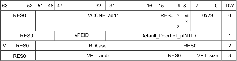
Image text
63 52 51 48 47 32 31 16 15 9 8 7 0 DW
RES0 VCONF_addr RES0 P All 0x29 0
T oc
Z
RES0 vPEID Default_Doorbell_pINTID 1
V RES0 RDbase RES0 2
RES0 VPT_addr RES0 VPT_size 3
In Figure 5-22:
-
RDbase = Identifies the target Redistributor. RES0 when V==0.
-
VCONF_addr = Bits [51:16] of the address of the vPE’s Virtual Configuration Table, bits [15:0] are 0. RES0 when V==0.
-
VPT_addr = Bits [51:16] of the address of the vPE’s Virtual Pending Table, bits [15:0] are 0. RES0 when V==0.
-
VPT_size = The number of bits of vINTID for the vPE. RES0 when V==0.
-
Default_Doorbell_pINTID is the default doorbell for the vPE. RES0 when V==0.
-
Alloc = Signifies whether this is the first map, or last unmap, for this vPEID.
-
PTZ = Signifies whether VPT_addr points at zeroed memory, ignored when V!=1 or Alloc!=1.
The command and its arguments are:
VMAPP vPEID, RDbase, VPT_addr, VPT_size, V
When V is 0:
- VMAPP removes the mapping for the specified vPE.
When V is 1:
- Behavior is UNPREDICTABLE if RDbase does not specify a valid Redistributor.
A command error occurs if any of the following apply:
-
vPEID exceeds the maximum number supported by the ITS, as defined by GITS_BASER
. -
Size exceeds the maximum value permitted by the settings of GITS_TYPER.ID_bits.
-
VMAPP with V==1 specifies a Default_Doorbell_pINTID value other than 1023 that is outside the implemented LPI range. The command error code reported is 0x01_2906 (VMAPP_PHYSICALID_OOR).
In this case, the ITS must take the actions described in Command errors.
Note If a system contains multiple ITSs, Arm strongly recommends that software does not issue a VMAPP when there is an outstanding VMOVP for the same vPEID on another ITS, as this could create a race condition.
For the pseudocode that describes the operation of this command, see VMAPP GICv4.0.
Use of of the V and Alloc fields
GICv4.1 introduces the vPE Configuration table, which is associated with the Redistributors that record the locations of the virtual LPI Configuration and Pending tables. This table is populated using the VMAPP command.
The Alloc field in a VMAPP command is used when vPEs are created or destroyed, to indicate when the vPE Configuration table entry should be updated.
A VMAPP with {V, Alloc}=={0, 1} cleans and invalidates any cached virtual Pending table and virtual Configuration table associated with the vPEID held in the GIC. Invalid use of the Alloc field can cause UNPREDICTABLE behavior, including continued access by the IRI.
For a VMAPP when V==1, VPT_size determines the size of the vINTID namespace, from which the size of the virtual Configuration and Pending tables are derived.
For a VMAPP with V==1, if VPT_size is greater than the supported INTID size, one of the following CONSTRAINED UNPREDICTABLE values are used:
-
The specified value.
-
An UNKNOWN value in range value.
A VMAPP with V==1, Default_Doorbell_pINTID==1023 indicates no default doorbell.
A VMAPP with V==1 that specifies one of the following values of Default_Doorbell_pINTID, causes UNPREDICTABLE behavior to occur:
-
The value is used for valid EventID or DeviceID mappings.
-
The value is for the default doorbell of an existing valid vPE.
A VMAPP with Alloc==0 indicates that there is an existing mapping on at least one ITS for the vPEID. If this is not true, the resulting behavior is UNPREDICTABLE. A VMAPP with {V, Alloc}=={1, 1} indicates that this is the first mapping of the vPEID, in any ITS. Setting {V, Alloc}=={1, 1} at any other time causes UNPREDICTABLE behavior.
A VMAPP with {V, Alloc}=={0, 1} indicates that this is the last mapping for the vPEID, in any ITS. Setting {V, Alloc}=={0, 1} at any other time causes UNPREDICTABLE behavior.
The virtual LPI Configuration table and virtual LPI Pending table are allocated to the IRI when VMAPP with {V, Alloc}=={1, 1} is issued, and remains allocated to the IRI until VMAPP with {V, Alloc}=={0, 1} is completed. Table 5-7 summarizes the effects of the V and Alloc field combinations.
Table 5-7 Effects of V and Alloc field combinations
| V | Alloc | Description |
|---|---|---|
| 0 | 0 | Unmapcommand, there is still at least one other ITS with a valid mapping. |
| 0 | 1 | Unmapcommand, no other ITS has a valid mapping. |
| 1 | 0 | Mapcommand, at least one other ITS already has this mapping. |
| 1 | 1 | Mapcommand, no other ITS has this mapping yet. |
Note UNPREDICTABLE behavior associated with the invalid use of Alloc can include the IRI continuing to read or write memory structures associated with the vPEID after release. Arm strongly recommends avoiding these cases.
A VMAPP with {V, Alloc}=={0, x} is self-synchronizing. This means the ITS command queue does not show the command as consumed until all of its effects are completed.
When multiple ITSs are implemented, issuing VMAPPs with V==1 for the same vPEID on different ITSs with different values of VCONF_addr, VPT_addr or VPT_size, causes UNPREDICTABLE behavior.
When multiple ITSs are implemented, issuing VMAPPs with {V, Alloc}=={1, 0} where Default_Doorbell_pINTID or RDbase does not match the currently configured value causes UNPREDICTABLE behavior.
When {V, Alloc}!={1, 1}, the PTZ bit is IGNORED.
When {V, Alloc, PTZ}=={1, 1, 0}:
-
The IMPLEMENTATION DEFINED region of the specified virtual Pending table must contain all zeros or have been populated by a GIC of the same implementation. Otherwise the behavior is UNPREDICTABLE.
-
The pending state and SGI configuration will be loaded by the IRI.
When {V, Alloc, PTZ}=={1, 1, 1}, the specified virtual Pending table must contain all zeros, otherwise the behavior is UNPREDICTABLE. This includes the SGI and IMPLEMENTATION DEFINED regions.
5.3.20 VMAPTI
This command maps the event defined by DeviceID and EventID into an ITT entry with vPEID and vINTID, and Dbell_pINTID, a doorbell provision.
Note
-
vINTID ≥0x2000 for a valid LPI INTID.
-
Dbell_pINTID must be either 1023 or Dbell_pINTID ≥0x2000 for a valid LPI INTID.
This command is provided only in GICv4.
Figure 5-23 shows the format of the VMAPTI command.
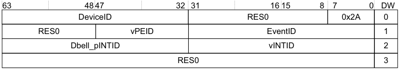
Image text
63 48 47 32 31 16 15 8 7 0 DW
DeviceID RES0 0x2A 0
RES0 vPEID EventID 1
Dbell_pINTID vINTID 2
RES0 3
In Figure 5-23:
-
vPEID specifies the vPE.
-
DeviceID specifies a device owned by the vPE.
-
vINTID specifies the INTID presented to the vPE that controls the device that DeviceID specifies.
-
Dbell_pINTID specifies the pINTID that is presented to the PE if the vPE is not scheduled.
Note If Dbell_pINTID is 1023 then no physical interrupt is generated.
- DW is the doubleword offset within a 32 byte, or four doubleword, ITS command packet.
If there is an existing mapping for the EventID-DeviceID combination, behavior is UNPREDICTABLE.
The command and its arguments are:
VMAPTI DeviceID, EventID, vINTID, Dbell_pINTID, vPEID
A command error occurs if any of the following apply:
-
DeviceID exceeds the maximum value supported by the ITS.
-
vPEID exceeds the maximum number supported by the ITS, as defined by GITS_BASER
. -
The device specified by DeviceID is not mapped to an ITT, using MAPD.
-
The EventID exceeds the maximum value allowed by the ITT. This value is specified by the Size field when the MAPD command is issued.
-
vINTID does not specify a valid LPI INTID, see INTIDs.
-
Dbell_pINTID does not specify a valid doorbell INTID, where a valid INTID is either: — 1023.
- Within the supported range for LPIs.
In this case, the ITS must take the actions described in Command errors.
The following pseudocode describes the operation of the VMAPTI command:
// ITS.VMAPTI // ==========
ITS.VMAPTI(ITSCommand cmd)
    if DeviceOutOfRange(cmd.DeviceID)
    then if GITS_TYPER.SEIS == '1'
    then IMPLEMENTATION_DEFINED "SError VMAPTI_DEVICE_OOR";
UNPREDICTABLE;
if VCPUOutOfRange(cmd.VCPUID) then
    if GITS_TYPER.SEIS == '1' then
        IMPLEMENTATION_DEFINED "SError VMAPTI_VCPU_OOR";
        UNPREDICTABLE;
    DeviceTableEntry dte = ReadDeviceTable(UInt(cmd.DeviceID));
    if !dte.Valid then
        if GITS_TYPER.SEIS == '1' then
            IMPLEMENTATION_DEFINED "SError VMAPTI_UNMAPPED_DEVICE";
            UNPREDICTABLE;
        if IdOutOfRange(cmd.EventID, dte.ITT_size) then
            if GITS_TYPER.SEIS == '1' then
                IMPLEMENTATION_DEFINED "SError VMAPTI_ID_OOR";
                UNPREDICTABLE;
            if LPIOutOfRange(cmd.vINTID) then
                if GITS_TYPER.SEIS == '1' then
                    IMPLEMENTATION_DEFINED "SError VMAPTI_VIRTUALID_OOR";
                    IncrementReadPointer();
                    return;
                if LPIOutOfRange(cmd.pINTID) then
                    if GITS_TYPER.SEIS == '1' then
                        IMPLEMENTATION_DEFINED "SError VMAPTI_PHYSICALID_OOR";
                        UNPREDICTABLE;
                    InterruptTableEntry ite = ReadTranslationTable(dte.ITT_base, UInt(cmd.EventID));
ite.Valid = TRUE; ite.Type = virtual_interrupt; ite.OutputID = cmd.vINTID; ite.DoorbellID = cmd.Dbell_pINTID; ite.VCPUID = cmd.VCPUID;
WriteTranslationTable(dte.ITT_base, UInt(cmd.EventID), ite);
IncrementReadPointer();
return;
5.3.21 VMOVI
This command updates the vPEID field in the ITT entry for the event defined by DeviceID and EventID. It also translates the event defined by EventID and DeviceID into a vPEID and pINTID, and instructs the appropriate Redistributor to move the pending state of the interrupt to the Redistributor defined by the new vPEID, and updates the ITE associated with the event to use the new vPEID.
This command is provided only in GICv4.
Figure 5-24 shows the format of the VMOVI command.
| 63 | 48 | 47 | 32 | 31 | 8 | 7 1 | 0 | DW | |
|---|---|---|---|---|---|---|---|---|---|
| DeviceID | RES0 | 0x21 | 0 | ||||||
| RES0 | vPEID | EventID | 1 | ||||||
| Dbell_pINTID | RES0 | D | 2 | ||||||
| RES0 | 3 |
Figure 5-24 VMOVI command format
In Figure 5-24:
-
vPEID specifies the vPE.
-
EventID identifies the interrupt, associated with a device and already mapped by the ITS, that is to be moved to a new target specified by vPEID.
-
D specifies whether the Dbell_pINTID field is valid.
-
DeviceID specifies the device that generates the interrupt.
-
Dbell_pINTID specifies the ID that is presented to the hypervisor if the vPE is not scheduled.
Note
If Dbell_pINTID is 1023 then no physical interrupt is generated.
- DW is the doubleword offset within a 32 byte, or four doubleword, ITS command packet.
The command and its arguments are:
VMOVI DeviceID, EventID, vPEID, [Dbell_pINTID]
A command error occurs if any of the following apply:
-
DeviceID exceeds the maximum value supported by the ITS.
-
vPEID exceeds the maximum number supported by the ITS, as defined by GITS_BASER
. -
The device specified by DeviceID is not mapped to an ITT, using MAPD.
-
The EventID exceeds the maximum value allowed by the ITT. This value is specified by the Size field when the MAPD command is issued.
-
The vPE is not mapped to a Redistributor, using VMAPP GICv4.0.
-
EventID corresponds to a physical LPI.
-
If D is 1 and pINTID does not specify a valid doorbell INTID, where a valid INTID is either: — 1023.
- Within the supported range for LPIs.
In this case, the ITS must take the actions described in Command errors.
Note If, after using VMOVI to move an interrupt from vPE A to vPE B, software moves the same interrupt again, a VSYNC command must be issued to vPE A between the moves to ensure correct behavior.
When VMOVI is issued targeting a vPE that is unmapped, or mapped to a Redistributor with LPIs disabled, behavior is CONSTRAINED UNPREDICTABLE with a choice of:
-
Clear the pending state of the moved LPI.
-
Pending state unchanged on the source vPE.
The following pseudocode describes the operation of the VMOVI command:
// ITS.VMOVI

// =========
ITS.VMOVI(ITSCommand cmd)
if DeviceOutOfRange(cmd.DeviceID) then
    if GITS_TYPER.SEIS == '1' then
        IMPLEMENTATION_DEFINED "SError VMOVI_DEVICE_OOR";
        UNPREDICTABLE;
    if VCPUOutOfRange(cmd.VCPUID) then
        if GITS_TYPER.SEIS == '1' then
            IMPLEMENTATION_DEFINED "SError VMOVI_VCPU_OOR";
            UNPREDICTABLE;
        if ( cmd.V == '1' && LPIOutOfRange(cmd.pINTID) && cmd.pINTID != '1023') then
            if GITS_TYPER.SEIS == '1' then
                IMPLEMENTATION_DEFINED "SError VMOVI_PHYSICALID_OOR";
                UNPREDICTABLE;
            DeviceTableEntry dte = ReadDeviceTable(UInt(cmd.DeviceID));
            if !dte.Valid then
                if GITS_TYPER.SEIS == '1' then
                    IMPLEMENTATION_DEFINED "SError VMOVI_UNMAPPED_DEVICE";
                    UNPREDICTABLE;
                if IdOutOfRange(cmd.EventID, dte.ITT_size) then
                    if GITS_TYPER.SEIS == '1' then
                        IMPLEMENTATION_DEFINED "SError VMOVI_ID_OOR";
                        UNPREDICTABLE;
                    InterruptTableEntry ite = ReadTranslationTable(dte.ITT_base, UInt(cmd.EventID));
                    if !ite.Valid then
                        if GITS_TYPER.SEIS == '1' then
                            IMPLEMENTATION_DEFINED "SError VMOVI_UNMAPPED_INTERRUPT";
                            UNPREDICTABLE;
                        if ite.Type == physical_interrupt then
                            if GITS_TYPER.SEIS == '1' then
                                IMPLEMENTATION_DEFINED "SError VMOVI_ID_IS_PHYSICAL";
                                UNPREDICTABLE;
                            VCPUTableEntry vte1 = ReadVCPUTable(UInt(ite.VCPUID));
                            VCPUTableEntry vte2 = ReadVCPUTable(UInt(cmd.VCPUID));
                            if !vte1.Valid then
                                if GITS_TYPER.SEIS == '1' then
                                    IMPLEMENTATION_DEFINED "SError VMOVI_ITEVCPU_INVALID";
                                    UNPREDICTABLE;
                                if !vte2.Valid then
                                    if GITS_TYPER.SEIS == '1' then
                                        IMPLEMENTATION_DEFINED "SError VMOVI_CMDVCPU_INVALID";
                                        UNPREDICTABLE;
                                    bits(32) rd1 = vte1.RDbase;
                                    Address vpt1 = vte1.VPT_base;
                                    bits(32) rd2 = vte2.RDbase;
                                    Address vpt2 = vte2.VPT_base;
ite.VCPUID = cmd.VCPUID;
// From this point new interrupts sent to the new VCPU move the pending
// state to rd2 if set taking care of any races where the interrupt
// has been forwarded to the processor
MoveVirtualPendingState(rd1, vpt1, vpt2, ite.OutputID);

IncrementReadPointer();

return;
5.3.22 VMOVP GICv4.0
This command updates the vPE table entry defined by vPEID to the target RDbase. Software must use SequenceNumber and ITSList to synchronize the execution of VMOVP commands across more than one ITS.
This command is provided only in GICv4.
Software must ensure that this command is not executed with a vPEID that is scheduled on the target Redistributor, otherwise system behavior is UNPREDICTABLE.
Figure 5-25 shows the format of the VMOVP command.
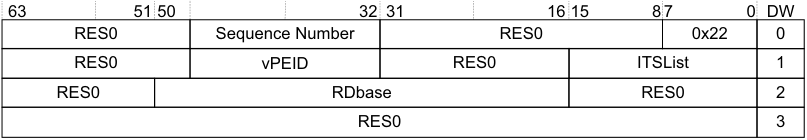
Image text
63 51 50 32 31 16 15 8 7 0 DW
RES0 Sequence Number RES0 0x22 0
RES0 vPEID RES0 ITSList 1
RES0 RDbase RES0 2
RES0 3
In Figure 5-25:
-
vPEID specifies the vPE.
-
RDbase specifies the Redistributor to which interrupts are forwarded. See IMPLEMENTATION DEFINED sizes in ITS command parameters.
-
Sequence Number specifies the identity of the synchronization point that every ITS included in ITS List uses. When GITS_TYPER.VMOVP == 0 Sequence Number specifies the identity of the synchronization point that is used by all ITSs that are included in ITSList.
-
When GITS_TYPER.VMOVP == 1 Sequence Number is RES0.
-
For more information, see VMOVP usage.
-
-
ITSList specifies the ITS instances that are included in the synchronization operation, where:
-
Each bit in ITS List identifies an ITS where bit[n] corresponds to ITS n.
-
An ITS is included if the corresponding bit is set to 1. When GITS_TYPER.VMOVP == 0 ITSList specifies which ITSs are included in the synchronization operation. Each bit of ITSList corresponds to an ITS, for example bit[0] of ITSList corresponds to ITS 0, bit[1] to ITS 1.
-
When GITS_TYPER.VMOVP ==1 ITSList is res0.
- DW is the doubleword offset within a 32 byte, or four doubleword, ITS command packet.
The command and its arguments are:
VMOVP, vPEID, RDbase, SequenceNumber, ITSList
A command error occurs if any of the following apply:
-
If the PE specified by vPEID is not mapped to a Redistributor, using VMAPP GICv4.0.
-
vPEID exceeds the maximum number supported by the ITS, as defined by GITS_BASER
.
In this case, the ITS must take the actions described in Command errors.
The following pseudocode describes the operation of the VMOVP command:
// ITS.VMOVP // ========= ITS.VMOVP(ITSCommand cmd)
if VCPUOutOfRange(cmd.VCPUID) then
    if GITS_TYPER.SEIS == '1' then
        IMPLEMENTATION_DEFINED "SError VMOVP_VCPU_OOR";
        UNPREDICTABLE;
    VCPUTableEntry vte = ReadVCPUTable(UInt(cmd.VCPUID));
    if !vte.Valid then
        if GITS_TYPER.SEIS == '1' then
            IMPLEMENTATION_DEFINED "SError VMOVP_VCPU_INVALID";
            UNPREDICTABLE;
vte.RDbase = cmd.RDbase;
if HasGIC41Ext() then UpdateVPEConfigurationTable(UInt(cmd.VCPUID), cmd.RDbase, cmd.Default_Doorbell_pINTID);

WriteVCPUTable(UInt(cmd.VCPUID), vte);

IncrementReadPointer();

return;
VMOVP usage
Where more than one ITS controls interrupts for the same vPE, moving this vPE must be coordinated between the different ITSs. This is controlled by software using one of the two approaches detailed here:
When GITS_TYPER.VMOVP == 0:
-
The VMOVP command must be issued for each ITS that controls interrupts for the vPE that is being moved. Each of these commands must have a common sequence number. That sequence number cannot be used for other VMOVP commands until all commands that previously used that sequence number have been processed by all ITSs.
-
The VMOVP command issued for each ITS contains a list of all the ITSs that are affected by moving the vPE. This is the ITS List.
-
Each ITS must have the sequence numbers presented to it in the same order in that they are presented to the other ITSs. When GITS_TYPER.VMOVP == 1:
-
The VMOVP command must be issued on only one of the ITSs that controls interrupts for the vPE that is being moved.
-
The implementation is responsible for propagating the updated mapping.
Not following this approach results in UNPREDICTABLE behavior.
Note If a system contains multiple ITSs, Arm strongly recommends that software does not issue a VMAPP when there is an outstanding VMOVP for the same vPEID on another ITS, as this could create a race condition.
5.3.23 VMOVP GICv4.1
The VMOVP command is modified in GICv4.1 to allow a Default Doorbell to be assigned to the vPE.
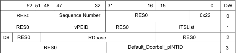
Image text
52 51 48 47 32 31 16 15 0 DW
RES0 Sequence Number RES0 0x22 0
RES0 vPEID RES0 ITSList 1
DB RES0 RDbase RES0 2
RES0 Default_Doorbell_pINTID 3
In Figure 5-26:
-
Default_Doorbell_pINTID is the default doorbell for the vPE.
-
DB signifies whether to mark the vPE as requiring a Default Doorbell on the target.
A VMOVP, Default_Doorbell_pINTID==1023 means no default doorbell. For a VMOVP with a valid Default_Doorbell_pINTID, other than 1023, the pending state of the default doorbell is transferred to the new target.
A VMOVP with Default_Doorbell_pINTID==1023 clears the pending state of the default doorbell on the old target if one was previously specified. The pending state of the default doorbell is transferred even when the INTID used for the doorbell is changed. Moving a vPE does not change the rules on generating default doorbells.
When VMOVP is issued, if DB==1, the vPE is marked as requesting Default Doorbell generation on the new target. When DB==0, the vPE is marked as not requesting Default Doorbell generation on the new target.
A command error occurs if any of the following apply:
-
The PE specified by vPEID is not mapped to a Redistributor, using VMAPP.
-
vPEID exceeds the maximum number supported by the ITS, as defined by GITS_BASER
. -
A VMOVP specifies a value of Default_Doorbell_pINTID outside of the implemented LPI range, other than 1023. The command error code reported is 0x01_2206(VMOVP_PHYSICALID_OOR).
In this case, the ITS must take the actions described in Command errors.
VMOVP usage in GICv4.1
VMOVP usage in GICv4.1 is the same as in GICv4.0. See VMOVP usage for more information.
5.3.24 VSGI for GICv4.1 only
The vSGI command sets the configuration of a specified vSGI and optionally clears its pending state.
Figure 5-27 shows the format of the vSGI command.
| 63 48 | 32 47 36 35 | 32 47 36 35 | 31 20 24 23:20 19: | 31 20 24 23:20 19: | 31 20 24 23:20 19: | 8 15:11 9 10 | 8 15:11 9 10 | 8 15:11 9 10 | 8 15:11 9 10 | 7 0 | DW |
|---|---|---|---|---|---|---|---|---|---|---|---|
| RES0 | vINTID | RES0 | Pri | RES0 | RES0 | G | C | E | 0x23 | 0 | |
| RES0 | vPEID | RES0 | 1 | ||||||||
| RES0 | 2 | ||||||||||
| RES0 | 3 |
Figure 5-27 vSGI command encoding
Where:
-
E is the enable configuration.
- Ignored when C==1.
-
G is the group configuration.
- Ignored when C==1.
-
Priority, records bits [7:4] of the priority configuration.
-
Bits [3:0] are treated as 0b0000.
-
Ignored when C==1.
-
-
vINTID and vPEID identify the interrupt.
-
C is used to indicate whether the pending state of the interrupt should be cleared.
The following pseudocode describes the operation of the VSGI command:
// ITS.VSGI // =========
ITS.VSGI(ITSCommand cmd)
    if VCPUOutOfRange(cmd.VCPUID)
    then if GITS_TYPER.SEIS == '1'
    then IMPLEMENTATION_DEFINED "SError VSGI_VCPU_OOR";
UNPREDICTABLE;
VCPUTableEntry vte = ReadVCPUTable(UInt(cmd.VCPUID));
// It is CONSTRAINED UNPREDICTABLE whether ReadVCPUTable() can
// return mappings from other ITSs when mapping exists on current
// current ITS

if Valid then
   if (CMD.C==0) then
        // Set configuration of interrupt
        SetVirtualSGIConfiguration(cmd.VCPUID, vte, cmd.Intid, cmd.E, cmd.Priority, cmd.G);
   else
        // Clear pending state of interrupt
        ClearVirtualSGIPendingState(VCPUID, vte, cmdIntid);

IncrementReadPointer();
return;
5.3.25 VSYNC
This command ensures all outstanding ITS operations for the vPEID specified are globally observed before any further ITS commands are executed. Following the execution of a VSYNC the effects of all previous commands must apply to subsequent writes to GITS_TRANSLATER.
This command is provided only in GICv4.
Figure 5-28 shows the format of the VSYNC command.
| 63 | 48 | 47 | 32 | 31 | 8 | 7 0 | DW | |
|---|---|---|---|---|---|---|---|---|
| RES0 | 0x25 | 0 | ||||||
| RES0 | vPEID | RES0 | 1 | |||||
| RES0 | 2 | |||||||
| RES0 | 3 |
Figure 5-28 VSYNC command format
In Figure 5-28:
-
vPEID specifies the vPE for which commands must be synchronized.
-
DW is the doubleword offset within a 32 byte, or four doubleword, ITS command packet.
The command and its arguments are:
VSYNC vPEID
A command error occurs if any of the following apply:
-
If the PE specified by vPEID is not mapped to a Redistributor, using VMAPP GICv4.0.
-
vPEID exceeds the maximum number supported by the ITS, as defined by GITS_BASER
.
In this case, the ITS must take the actions described in Command errors.
The following pseudocode describes the operation of the VSYNC command:
// ITS.VSYNC // ========= ITS.VSYNC(ITSCommand cmd)
    if VCPUOutOfRange(cmd.VCPUID)
    then if GITS_TYPER.SEIS == '1'
    then IMPLEMENTATION_DEFINED "SError VSYNC_VCPU_OOR";
UNPREDICTABLE;

VCPUTableEntry vte = ReadVCPUTable(UInt(cmd.VCPUID));

if !vte.Valid then if GITS_TYPER.SEIS == '1' then IMPLEMENTATION_DEFINED "SError VSYNC_VCPU_INVALID"; UNPREDICTABLE;

bits(32) rd_base = vte.RDbase;

// Wait
    for the external effects of any virtual commands to be observable by all redistributors
// and ensure the internal effects of any previous commands affect any subsequent interrupt
// requests or commands WaitForVirtualCompletion(rd_base);

IncrementReadPointer();

return;
5.4 Common ITS pseudocode functions
The following terminology appears in some of the pseudocode functions in this section:
Interrupt Translation
An action that causes the ITS to attempt to set a particular pending bit in a particular table. Pending Interrupt
A particular pending bit is set in a particular table.
The pseudocode functions in this section are based on the following assumptions:
-
Each ITS function must be performed as an atomic operation. Implementations must ensure that the observed behavior is consistent with that from a strictly atomic implementation.
-
Where the pseudocode issues a sequence of read and write operations to a particular Redistributor, these operations must be performed in the order in which they were generated.
-
Where the pseudocode issues a write to a particular Redistributor, operation does not need to wait for the completion of the write.
-
Where the pseudocode issues write to memory to update a table, operation does not need to wait for the completion of these writes. A write to memory might never become visible to an external observer. However, the effect of any such writes must be ordered by any subsequent ITS operations, including the handling of interrupt translations. There are no ordering rules other than the standard rule that memory must appear as if writes to each location occurred in program order.
-
Because each ITS function is performed as an atomic operation, any new interrupt translation that occurs after the function must be subject to the effects of that function.
-
The effects of caching of the Redistributor LPI Configuration and LPI Pending tables are specified explicitly in the pseudocode.
-
An interrupt translation might set a pending bit and pending bits remain set until handled by the PE. While an interrupt is pending it might be affected by an interrupt translation that is updated by a subsequent ITS function.
Note Some variable names used in the pseudocode differ from those used in the body text. For a list of the affected variables, see _Pseudocode terminology_B-910.
The following pseudocode invalidates any associated caching for the LPI configuration in the Redistributor for the specified translation.
// InvalidateByITE
// ===============
boolean InvalidateByITE(InterruptTableEntry ite)
if ite.Type == physical_interrupt then
    CollectionTableEntry cte = ReadCollectionTable(UInt(ite.ICID));
    if !cte.Valid then
        return FALSE;
    InvalidateInterruptCaches(ite.ICID, ite.OutputID);
else

VCPUTableEntry vte = ReadVCPUTable(UInt(ite.VCPUID));
if !vte.Valid then
    return FALSE;
InvalidateVirtualInterruptCaches(ite.VCPUID, ite.OutputID);
return TRUE;
The following pseudocode describes moving a pending interrupt.
The following pseudocode describes moving a pending interrupt.
// MovePendingState()
// ==================

MovePendingState(bits(32) rd1, bits(32) rd2, bits(32) ID)
    if IsPending(GICR_PENDBASER[rd1], ID) then
        // The interrupt is pending in the source redistributor

        // Make sure the interrupt is released or taken by the processor for
        // example by sending a clear and waiting for the response
        EnsureInterruptNotPendingOnProcessor(rd1, ID);

        if IsPending(GICR_PENDBASER[rd1], ID) then
            // The CPU released the interrupt and it is still pending
            // Note: the following must be done without any possibility of the
            // source redistributor re-forwarding the interrupt to the processor
            ClearPendingStateLocal(GICR_PENDBASER[rd1], ID);
            SetPendingStateLocal(GICR_PENDBASER[rd2], ID);

The following pseudocode describes moving a pending virtual interrupt.

// MoveVirtualPendingState()
// =========================

MoveVirtualPendingState(bits(32) rd_base, Address vpt1, Address vpt2, bits(32) ID)
    if IsPending(vpt1, ID) then
        // The interrupt is pending in the source redistributor

        // Make sure the interrupt is released or taken by the processor for example by sending a
        // VClear and waiting for the response
        EnsureVirtualInterruptNotPendingOnProcessor(rd_base, vpt1, ID);

        if IsPending(vpt1, ID) then
            // The CPU released the interrupt and it is still pending
            // Note: the following must be done without any possibility of the source redistributor
            // re-forwarding the interrupt to the processor
            ClearVirtualPendingStateLocal(vpt1, ID);
            SetVirtualPendingStateLocal(vpt2, ID);
    return;

The following pseudocode describes invalidating the caching of configuration data for the default doorbell
associated with a vPE.

// Invalidates any caching of configuration for the default
// doorbell associated with a vPE
InvalidateInterruptDoorbellCaches(UInt VCPUID, VCPUTableEntry vte);

// Sets the configuration of the specified vSGI
SetVirtualSGIConfiguration(UInt VCPUID, VCPUTableEntry vte, UInt Intid,
                           UInt Enable, UInt Priority, UInt Group);

// Clears the pending state of the specified vSGI
ClearVirtualSGIPendingState(UInt VCPUID, VCPUTableEntry vte, UInt Intid);

// Returns TRUE if the ITS supports GICv4.1
Boolean HasGIC41Ext();
The following pseudocode describes moving a pending virtual interrupt.
// MoveVirtualPendingState() // =========================
// The names of the Banked core registers.

enumeration RName {RName_0usr, RName_1usr, RName_2usr, RName_3usr, RName_4usr, RName_5usr,
                   RName_6usr, RName_7usr, RName_8usr, RName_8fiq, RName_9usr, RName_9fiq,
                   RName_10usr, RName_10fiq, RName_11usr, RName_11fiq, RName_12usr, RName_12fiq,
                   RName_SPusr, RName_SPfiq, RName_SPirq, RName_SPsvc,
                   RName_SPabt, RName_SPund, RName_SPmon, RName_SPhyp,
                   RName_LRusr, RName_LRfiq, RName_LRirq, RName_LRsvc,
                   RName_LRabt, RName_LRund, RName_LRmon,
                   RName_PC};

array bits(8) _Memory[0..0xFFFFFFFF];

Arrays are always explicitly declared, and there is no notation for a constant array. Arrays always contain at least
one element, because:
•      Enumerations always contain at least one symbolic constant.
•      Integer ranges always contain at least one integer.

Arrays do not usually appear directly in pseudocode. The items that syntactically look like arrays in pseudocode are
usually array-like functions such as R[i], MemU[address, size] or Elem[vector, i, size]. These functions package
up and abstract additional operations normally performed on accesses to the underlying arrays, such as register
banking, memory protection, endian-dependent byte ordering, exclusive-access housekeeping and Advanced SIMD
element processing.
The following pseudocode describes invalidating the caching of configuration data for the default doorbell associated with a vPE.
// Invalidates any caching of configuration for interrupts which are
// members of the collection specified by "collection"

InvalidateCollectionCaches(integer collection);
5.4.1 ITS helper functions
This subsection describes the ITS helper functions. These functions are placeholder functions for behavior that is not architected and that is IMPLEMENTATION DEFINED.
The functions are indicated by the hierarchical path names, for example shared/gic/its/its_helper:
-
shared/gic/its/its_helper/Address.
-
shared/gic/its/its_helper/ClearPendingState.
-
shared/gic/its/its_helper/ClearPendingStateLocal.
-
shared/gic/its/its_helper/CollectionOutOfRange.
-
shared/gic/its/its_helper/CollectionTableEntry.
-
shared/gic/its/its_helper/DeviceOutOfRange.
-
shared/gic/its/its_helper/DeviceTableEntry.
-
shared/gic/its/its_helper/EndOfCommand.
-
shared/gic/its/its_helper/EnsureInterruptNotPendingOnProcessor.
-
shared/gic/its/its_helper/EnsureVirtualInterruptNotPendingOnProcessor.
-
shared/gic/its/its_helper/IdOutOfRange.
-
shared/gic/its/its_helper/IncrementReadPointer.
-
shared/gic/its/its_helper/InterruptTableEntry.
-
shared/gic/its/its_helper/InterruptType.
-
shared/gic/its/its_helper/InterruptType.
-
shared/gic/its/its_helper/InvalidateInterruptCaches.
-
shared/gic/its/its_helper/InvalidateInterruptConfigurationCaches.
-
shared/gic/its/its_helper/InvalidateVCPUCaches.
-
shared/gic/its/its_helper/InvalidateVirtualConfigurationCaches.
-
shared/gic/its/its_helper/InvalidateVirtualInterruptCaches.
-
shared/gic/its/its_helper/IsPending.
-
shared/gic/its/its_helper/IsPending.
-
shared/gic/its/its_helper/LPIOutOfRange.
-
shared/gic/its/its_helper/MoveAllPendingState.
-
shared/gic/its/its_helper/ReadCollectionTable.
-
shared/gic/its/its_helper/ReadDeviceTable.
-
shared/gic/its/its_helper/ReadTranslationTable.
-
shared/gic/its/its_helper/ReadVCPUTable.
-
shared/gic/its/its_helper/RetargetVirtualInterrupt.
-
• shared/gic/its/its_helper/SetPendingState.
-
shared/gic/its/its_helper/SetPendingStateLocal.
-
shared/gic/its/its_helper/SizeOutOfRange.
-
shared/gic/its/its_helper/VCPUOutOfRange.
-
shared/gic/its/its_helper/VCPUTableEntry.
-
shared/gic/its/its_helper/WaitForCompletion.
-
shared/gic/its/its_helper/WaitForVirtualCompletion.
-
• shared/gic/its/its_helper/WriteCollectionTable. • shared/gic/its/its_helper/WriteDeviceTable.
-
shared/gic/its/its_helper/WriteTranslationTable.
-
• shared/gic/its/its_helper/WriteVCPUTable.
shared/gic/its/its_helper/Address
// Address()
// ============

type Address = bits(48);
shared/gic/its/its_helper/ClearPendingState
// ClearPendingState()
// ===================
boolean ClearPendingState(InterruptTableEntry ite)
if ite.Type == physical_interrupt then
    CollectionTableEntry cte = ReadCollectionTable(UInt(ite.ICID));
    if (!cte.Valid) then
        return FALSE;
    bits(32) rd_base = cte.RDbase;
    ClearPendingStateLocal(GICR_PENDBASER[rd_base], ite.OutputID);
else
VCPUTableEntry vte = ReadVCPUTable(UInt(ite.VCPUID));
if (!vte.Valid) then
    return FALSE;
bits(32) rd_base = vte.RDbase;
Address vpt = vte.VPT_base;
ClearPendingStateLocal(vpt, ite.OutputID);
return TRUE;
shared/gic/its/its_helper/ClearPendingStateLocal
// ClearPendingStateLocal()
// =============================

// Clears the pending state of the physical interrupt specified by INTID
// for the redistributor which owns the LPI pending table specified by PendBase

ClearPendingStateLocal(PBType PendBase, bits(32) INTID);

// ClearVirtualPendingStateLocal()
// ============================

// Clears the pending state of the virtual interrupt specified by vINTID
// in the LPI pending table specified by base

ClearPendingStateLocal(Address base, bits(32) vINTID);
shared/gic/its/its_helper/CollectionOutOfRange
// CollectionOutOfRange()
// ================================

// Returns TRUE if the value supplied has bits above the implemented range
// or if the value exceeds the total number of collections supported in
// hardware and external memory

boolean CollectionOutOfRange(bits(16) collection);
shared/gic/its/its_helper/CollectionTableEntry
//CollectionTableEntry() // =======================
type CollectionTableEntry is ( boolean Valid, bits(32) RDbase )
shared/gic/its/its_helper/DeviceOutOfRange
// DeviceOutOfRange()
// =====================

// Returns TRUE if the value supplied has bits above the implemented range
// or if the value supplied exceeds the maximum configured size in the
// appropriate GITS_BASER<n>

boolean DeviceOutOfRange(bits(32) device);
shared/gic/its/its_helper/DeviceTableEntry
// DeviceTableEntry()
// =============

type DeviceTableEntry is (
    boolean Valid,
    Address ITT_base,
    bits(5) ITT_size
)
shared/gic/its/its_helper/EndOfCommand
// EndOfCommand()
// ================

// Terminate processing of the current command without incrementing the read pointer.
// This means the command will be run again.

EndOfCommand();
shared/gic/its/its_helper/EnsureInterruptNotPendingOnProcessor
// EnsureInterruptNotPendingOnProcessor()
// ======================================

// Returns when the physical interrupt specified by ID is not pending on
// the CPU interface connected to the redistributor specified by rd1

EnsureInterruptNotPendingOnProcessor(bits(32) rd1, bits(32) ID);
shared/gic/its/its_helper/EnsureVirtualInterruptNotPendingOnProcessor
// EnsureVirtualInterruptNotPendingOnProcessor()
// ==========================================

// Returns when the virtual interrupt specified by ID is not pending on
// the CPU interface connected to the redistributor specified by rd1

EnsureVirtualInterruptNotPendingOnProcessor(bits(32) rd1, Address vpt, bits(32) ID);
shared/gic/its/its_helper/IdOutOfRange
// IdOutOfRange()
// ============================

// Returns TRUE if the value supplied has bits above the implemented size or above the ITT_size

boolean IdOutOfRange(bits(32) ID, bits(5) ITT_size);
shared/gic/its/its_helper/IncrementReadPointer
// IncrementReadPointer()
// ===================

//Increments GITS_CREADR, wrapping if appropriate

IncrementReadPointer();
shared/gic/its/its_helper/InterruptTableEntry
// InterruptTableEntry()
// =====================

type InterruptTableEntry is (
boolean Valid,
InterruptType Type,
bits(32) OutputID,
bits(32) DoorbellID,
bits(16) ICID,
bits(16) VCPUID
)
shared/gic/its/its_helper/InterruptType
// InterruptType
// ====================

enumeration InterruptType { virtual_interrupt, physical_interrupt };
shared/gic/its/its_helper/InvalidateCollectionCaches
//InvalidateCollectionCaches() // =========================
// Invalidates any caching of configuration for interrupts which are // members of the collection specified by "collection"

InvalidateCollectionCaches(integer collection);
shared/gic/its/its_helper/InvalidateInterruptCaches
// InvalidateInterruptCaches()
// =============================

// Invalidates any caching of configuration for the physical
// interrupt specified by interruptID , which is a member of
// the collection specified by collection

InvalidateInterruptCaches(bits(16) collection, bits(32) interruptID);
shared/gic/its/its_helper/InvalidateInterruptConfigurationCaches
// InvalidateInterruptConfigurationCaches()
// ===================================

InvalidateInterruptConfigurationCaches(bits(32) ID, integer collection);
shared/gic/its/its_helper/InvalidateVCPUCaches
// InvalidateVCPUCaches()
// ==========================

// Invalidates any caching of configuration for the vPE specificed by vcpu_id

InvalidateVCPUCaches(integer vcpu_id);
shared/gic/its/its_helper/InvalidateVirtualConfigurationCaches
// InvalidateVirtualConfigurationCaches
// ================================

InvalidateVirtualConfigurationCaches(bits(32) ID, bits(16) VCPU);
shared/gic/its/its_helper/InvalidateVirtualInterruptCaches
// InvalidateVirtualInterruptCaches()
// =====================================

// Invalidates any caching of configuration for the virtual interrpt specified
// by the interruptID for the vPE specified by vcpi_id

InvalidateVirtualInterruptCaches(bits(16) vcpu_id, bits(32) interruptID);
shared/gic/its/its_helper/IsPending
// IsPending()
// ========================

// Returns TRUE if the virtual interrupt specified by interruptID
// is pending in the LPI pending table specified by base

boolean IsPending(Address base, bits(32) interruptID);
shared/gic/its/its_helper/IsPending
// IsPending()

// ========================
// Returns TRUE if the value supplied has bits above the implemented range or
// if the value supplied exceeds the maximum configured size in the
// appropriate GITS_BASERn

boolean VCPUOutOfRange(bits(16) vcpu);
shared/gic/its/its_helper/LPIOutOfRange
//LPIOutOfRange()
// ==========================
// Returns TRUE if the value supplied is larger than that permitted by GICD_TYPER.IDbits or not in the // LPI range and is not 1023

boolean LPIOutOfRange(bits(32) ID);
shared/gic/its/its_helper/MoveAllPendingState
// MoveAllPendingState()
// ===================

// Moves the pending state of all interrupts from the Redistributor specified by rd1
// to the Redistributor specified by rd2

MoveAllPendingState(bits(32) rd1, bits(32) rd2);
shared/gic/its/its_helper/ReadCollectionTable
// ReadCollectionTableEntry()
// =========================

// Reads a collection table entry from memory

CollectionTableEntry ReadCollectionTable(integer index);
shared/gic/its/its_helper/ReadDeviceTable
// ReadDevicePointer()
// ==========================

// Reads a device table entry from memory

DeviceTableEntry ReadDeviceTable(integer index);
shared/gic/its/its_helper/ReadTranslationTable
// ReadTranslationTable()
// =======================
// Reads a VCPU table entry from memory

VCPUTableEntry ReadVCPUTable(integer index);
shared/gic/its/its_helper/ReadVCPUTable
//ReadVCPUTable() // ===========================
// Reads a VCPU table entry from memory

VCPUTableEntry ReadVCPUTable(integer index);
shared/gic/its/its_helper/RetargetVirtualInterrupt
// RetargetVirtualInterrupt()
// =======================

RetargetVirtualInterrupt(integer device, bits(32) ID, integer vcpu);
shared/gic/its/its_helper/SetPendingState
// SetPendingState()
// =================

boolean SetPendingState(InterruptTableEntry ite)

     if ite.Type == physical_interrupt then
         CollectionTableEntry cte = ReadCollectionTable(UInt(ite.ICID));

         if !cte.Valid then
             return FALSE;

         bits(32) rd_base = cte.RDbase;

         SetPendingStateLocal(GICR_PENDBASER[rd_base], ite.OutputID);

     else
         VCPUTableEntry vte = ReadVCPUTable(UInt(ite.VCPUID));

         if !vte.Valid then
             return FALSE;

         bits(32) rd_base = vte.RDbase;
         Address vpt = vte.VPT_base;

         SetVirutalPendingStateLocal(vpt, ite.OutputID);

         if (GICR_VPENDBASER[rd_base].Valid == '1' &&
             GICR_VPENDBASER[rd_base].PhysicalAddress != vpt<47:16>) then
             if ite.DoorbellID != ZeroExtend(INTID_SPURIOUS, 32) then
                 // Not resident so set the doorbell interrupt pending as well
                 SetPendingStateLocal(GICR_PENDBASER[rd_base], ite.DoorbellID);

     return TRUE;
shared/gic/its/its_helper/SetPendingStateLocal
// SetPendingStateLocal()
// =======================

// Sets the pending state of the physical interrupt specified by INTID
// for the Redistributor that owns the LPI pending table specified by PendBase

SetPendingStateLocal(PBType PendBase, bits(32) INTID);

// SetVirtualPendingStateLocal()
// =======================

// Sets the pending state of the virtual interupt specified by INTID
// in the LPI pending table specified by base

SetPendingStateLocal(Address base, bits(32)INTID);
shared/gic/its/its_helper/SizeOutOfRange
// SizeOutOfRange()
// =====================

// Returns TRUE if the value supplied exceeds the maximum allowed by GITS_TYPER.ID_bits

boolean SizeOutOfRange(bits(5) ITT_size);
shared/gic/its/its_helper/VCPUOutOfRange
// VCPUOutOfRange()
// =======================
shared/gic/its/its_helper/VCPUTableEntry
//VCPUTableEntry() // ==================
type VCPUTableEntry is ( boolean Valid, bits(32) RDbase, Address VPT_base, bits(5) VPT_size )
shared/gic/its/its_helper/WaitForCompletion
// WaitForCompletion()
// ============================

// Returns when all external effects of any phsical commands are observable
// by all Redistributors and the internal effects of any previous
// commands affect any subsequent interrupt requests or commands

WaitForCompletion(bits(32) RDbase);
shared/gic/its/its_helper/WaitForVirtualCompletion
// WaitForVirtualCompletion()
// =======================

WaitForVirtualCompletion(bits(32) RDbase);
shared/gic/its/its_helper/WriteCollectionTable
//WriteCollectionTable() // =========================
// Writes a collection table entry to memory

WriteCollectionTable(integer index, CollectionTableEntry cte);
shared/gic/its/its_helper/WriteDeviceTable
// WriteDeviceTable()
// ========================

// Writes a device table entry to memory

WriteDeviceTable(integer index, DeviceTableEntry dte);
shared/gic/its/its_helper/WriteTranslationTable
// WriteTranslationTable()
// ================================

// Writes an ITT table entry to memory

WriteTranslationTable(Address base, integer index, InterruptTableEntry cte);
shared/gic/its/its_helper/WriteVCPUTable
// WriteVCPUTable()
// ===============================

// Writes a VCPU table entry to memory

WriteVCPUTable(integer index, VCPUTableEntry vte);
5.5 ITS command error encodings
When an ITS supports system errors, that is when GITS_TYPER.SEIS == 1, ITS command errors can be reported to software. It is IMPLEMENTATION DEFINED how these errors are recorded and reported.
Table 5-8 shows the ITS command error encodings.
| Table 5-8 ITS command error encodings | Table 5-8 ITS command error encodings |
|---|---|
| Encoding Error mnemonic Command | Error description |
| 0x01_0801 MAPD_DEVICE_OOR MAPD 0x01_0802 MAPD_ITTSIZE_OOR | Out of range |
| 0x01_0903 MAPC_COLLECTION_OOR MAPC | Out of range |
| 0x01_0B01 MAPI_DEVICE_OOR MAPI 0x01_0B03 MAPI_COLLECTION_OOR 0x01_0B04 MAPI_UNMAPPED_DEVICE 0x01_0B05 MAPI_ID_OOR | Unmapped device Out of range |
| 0x01_0A01 MAPTI_DEVICE_OOR MAPTI 0x01_0A03 MAPTI_COLLECTION_OOR 0x01_0A04 MAPTI_UNMAPPED_DEVICE 0x01_0A05 MAPTI_ID_OOR 0x01_0A06 MAPTI_PHYSICALID_OOR | Unmapped device Out of range |
| 0x01_0101 MOVI_DEVICE_OOR MOVI 0x01_0103 MOVI_COLLECTION_OOR 0x01_0104 MOVI_UNMAPPED_DEVICE 0x01_0105 MOVI_ID_OOR 0x01_0107 MOVI_UNMAPPED_INTERRUPT 0x01_0108 MOVI_ID_IS_VIRTUAL 0x01_0109 MOVI_UNMAPPED_COLLECTION | Unmapped device Out of range Unmapped interrupt vINTID specified Unmapped interrupt collection |
| 0x01_0F01 DISCARD_DEVICE_OOR DISCARD 0x01_0F04 DISCARD_UNMAPPED_DEVICE 0x01_0F05 DISCARD_ID_OOR 0x01_0F07 DISCARD_UNMAPPED_INTERRUPT 0x01_0F10 DISCARD_ITE_INVALID | Out of range Unmapped device Out of range Unmapped interrupt Invalid translation table entry |
| Table 5-8 ITS command error encodings (continued) |
| Encoding Error mnemonic Command | Error description |
|---|---|
| 0x01_0C01 INV_DEVICE_OOR INV 0x01_0C04 INV_UNMAPPED_DEVICE 0x01_0C05 INV_ID_OOR 0x01_0C07 INV_UNMAPPED_INTERRUPT 0x01_0C10 INV_ITE_INVALID | Out of range Unmapped device Out of range Unmapped interrupt Invalid translation table entry |
| 0x01_0D03 INVALL_COLLECTION_OOR INVALL 0x01_0D09 INVALL_UNMAPPED_COLLECTION | Out of range Unmapped interrupt collection |
| 0x01_0301 INT_DEVICE_OOR INT 0x01_0304 INT_UNMAPPED_DEVICE 0x01_0305 INT_ID_OOR 0x01_0307 INT_UNMAPPED_INTERRUPT 0x01_0310 INT_ITE_INVALID | Out of range Unmapped device Out of range Unmapped interrupt Invalid translation table entry |
| 0x01_0501 CLEAR_DEVICE_OOR CLEAR 0x01_0504 CLEAR_UNMAPPED_DEVICE 0x01_0505 CLEAR_ID_OOR 0x01_0507 CLEAR_UNMAPPED_INTERRUPT 0x01_0510 CLEAR_ITE_INVALID | Out of range Unmapped device Out of range Unmapped interrupt Invalid translation table entry |
| 0x01_2906 VMAPP_PHYSICALID_OOR VMAPP GICv4.0or VMAPP GICv4.1 0x01_2911 VMAPP_VCPU_OOR 0x01_2912 VMAPP_VPTSIZE_OOR | Out of range |
| Table 5-8 ITS command error encodings (continued) |
| Encoding Error mnemonic Command | Error description |
|---|---|
| 0x01_2b01 VMAPI_DEVICE_OOR VMAPI 0x01_2b11 VMAPI_VCPU_OOR 0x01_2b04 VMAPI_UNMAPPED_DEVICE 0x01_2b05 VMAPI_ID_OOR 0x01_2b06 VMAPI_PHYSICALID_OOR | Out of range Unmapped device Out of range |
| 0x01_2a01 VMAPTI_DEVICE_OOR VMAPTI 0x01_2a11 VMAPTI_VCPU_OOR 0x01_2a04 VMAPTI_UNMAPPED_DEVICE 0x01_2a05 VMAPTI_ID_OOR 0x01_2a13 VMAPTI_VIRTUALID_OOR 0x01_2a06 VMAPTI_PHYSICALID_OOR | Unmapped device Out of range |
| 0x01_2d11 VINVALL_VCPU_OOR VINVALL 0x01_2d14 VINVALL_VCPU_INVALID | Invalid vPE specified |
| 0x01_2511 VSYNC_VCPU_OOR VSYNC 0x01_2514 VSYNC_VCPU_INVALID | Out of range Invalid vPE specified |
| 0x01_2206 VMOVP_PHYSICALID_OOR VMOVP GICv4.0or VMOVP GICv4.1 0x01_2211 VMOVP_VCPU_OOR 0x01_2214 VMOVP_VCPU_INVALID | Out of range Invalid vPE specified |
| 0x01_2101 VMOVI_DEVICE_OOR VMOVI 0x01_2103 VMOVI_VCPU_OOR 0x01_2104 VMOVI_UNMAPPED_DEVICE 0x01_2105 VMOVI_ID_OOR 0x01_2106 VMOVI_PHYSICALID_OOR 0x01_2107 VMOVI_UNMAPPED_INTERRUPT 0x01_2115 VMOVI_ID_IS_PHYSICAL 0x01_2116 VMOVI_ITEVCPU_INVALID 0x01_2117 VMOVI_CMDVCPU_INVALID | Out of range Unmapped device Out of range |
| Unmapped interrupt pINTID specified Invalid translation table entry Invalid vPE specified | |
| 0x01_2311 VSGI_VCPU_OOR VSGI for GICv4.1 only | vPEID greater than the configured range for the ITS. |
| 0x01_2E11 INVDB_VCPU_OOR INVDB GICv4.1 only | Out of range |
5.6 ITS power management
This subsection describes the software sequences for enabling and disabling an ITS. It contains the following sections:
-
Enabling an ITS .
-
Disabling an ITS .
5.6.1 Enabling an ITS
On power up, an ITS is reset to the quiescent state where GITS_CTLR.Quiescent == 1 and GITS_CTLR.Enabled == 0. To enable an ITS, software must:
-
Ensure any memory structures required to support the device, interrupt translation, interrupt collection, or virtual CPU tables are initialized or restored.
-
Ensure that the ITS command queue has been provisioned.
-
Set GITS_CTLR.Enabled to 1.
-
Configure the ITS as required using the appropriate ITS commands. For more information about the ITS commands, see ITS commands.
5.6.2 Disabling an ITS
To disable an ITS, software must:
-
Ensure that all interrupts that target the ITS that is being powered down are either redirected or disabled.
-
Disable the ITS by clearing GITS_CTLR.Enable to 0. The disabled ITS completes all outstanding operations and then sets GITS_CTLR.Quiescent to 1.
-
Ensure the ITS is quiescent by polling until GITS_CTLR.Quiescent == 1.
When GITS_CTLR.Enable == 0, write accesses to GITS_TRANSLATER are ignored. When GITS_CTLR.Quiescent == 1, all operations have completed and memory backed state is committed. The ITS can then be powered down to an IMPLEMENTATION DEFINED state.
Chapter 6: Virtual Interrupt Handling and Prioritization
This chapter describes the fundamental aspects of GIC virtual interrupt handling and prioritization:
-
About GIC support for virtualization .
-
Operation overview .
-
Configuration and control of VMs .
-
Pseudocode .
6.1 About GIC support for virtualization
An operating system that is executing at EL1 under the control of a hypervisor executing at EL2 is sometimes referred as a virtual machine (VM). A VM can support multiprocessing, which means that multiple virtual PEs (vPEs), that are scheduled by the hypervisor are executing on one or more physical PEs. When a vPE is executing on a PE, that vPE of the VM is referred to as being scheduled on the physical PE.
In Armv8, when EL2 is implemented and enabled, the CPU interface provides mechanisms to minimize the hypervisor overhead of routing interrupts to a VM. For more information about vPEs, see Operation overview .
For more information about EL2 and virtual interrupts, see Arm[®] Architecture Reference Manual, Armv8, for Armv8-A architecture profile .
In GICv4, for the directly injected virtual LPIs, the scheduled vPE is determined by GICR_VPENDBASER. For more information, see Doorbell interrupts .
Note The GIC does not provide additional mechanisms for the virtualization of the GICD_, GICR_, and GITS_* registers. To virtualize VM accesses to these registers, the hypervisor must set stage 2 Data Aborts to those memory locations so that the hypervisor can emulate these effects. For more information about stage 2 Data Aborts, see Arm[®] Architecture Reference Manual, Armv8, for Armv8-A architecture profile .
When a GIC provides support for virtualization, the VM operates in an environment that has the following features:
-
The vPE can be configured to receive virtual Group 0 interrupts.
-
The vPE can be configured to receive virtual Group 1 interrupts.
-
Virtual Group 0 interrupts are signaled using the virtual FIQ signal to Non-secure EL1.
-
Virtual Group 1 interrupts are signaled using the virtual IRQ signal to Non-secure EL1.
-
Virtual interrupts can be handled by the vPE as if they were physical interrupts.
Note
This applies when affinity routing and System register access are enabled. For information about support for virtual interrupts in legacy operation, see Support for legacy operation of VMs .
EL2 controls the generation of virtual interrupts for a VM. This allows software executing at EL2 to:
-
Generate virtual Group 0 and Group 1 interrupts for the vPE.
-
Save and restore the interrupt state of the vPE.
-
Control the prioritization of the virtual interrupts.
-
Change the vPE that is scheduled.
GICv4 introduces the ability to present virtual LPIs from an ITS directly to a vPE, without hypervisor intervention.
Handling virtual interrupts in legacy operation requires a GICV_* memory-mapped interface. See Support for legacy operation of VMs for more information.
6.2 Operation overview
GICv3 supports the Armv8-A virtualization functionality. A hypervisor executing at EL2 uses the ICH_* System register interface to configure and control a virtual PE (vPE) executing at EL1. For information about the VM control interface, see Configuration and control of VMs . A vPE uses the ICC_*_EL1 System register interface to communicate with the GIC. The configuration of HCR_EL2.{IMO, FMO} determines whether the virtual or the physical interface registers are accessed.
Note This chapter describes the handling of virtual interrupts in the context of the AArch64 state with System register access enabled. The individual AArch64 System register descriptions that are cross-referenced in this chapter contain a reference to the AArch32 System register that provides the same functionality. For information about VMs in legacy operation, see Support for legacy operation of VMs .
Software executing at EL3 or EL2 configures the PE to route physical interrupts to EL2. The interrupt can be:
-
An interrupt targeting a vPE. The hypervisor sets the corresponding virtual INTID to the pending state on the target vPE and includes the information about the associated physical INTID. When the vPE is not scheduled on a PE, the hypervisor might choose to reschedule the vPE. Otherwise the interrupt is left pending on the vPE for scheduling by the hypervisor at a later time.
-
An interrupt targeting the hypervisor. This interrupt might:
-
Have been generated by the system.
-
Be a maintenance interrupt associated with a scheduled VM. See Maintenance interrupts for more details.
-
In GICv4, be a doorbell interrupt from an ITS. In GICv4, a virtual interrupt can be presented to a vPE without hypervisor involvement. A doorbell interrupt must be generated when a virtual interrupt is made pending for a vPE but the vPE is not scheduled on a PE.
-
The hypervisor handles physical interrupts according to the rules described in Chapter 4 Physical Interrupt Handling and Prioritization before they are virtualized. For information about the handling of physical interrupts and their virtualization during legacy operation, see Chapter 14 Legacy Operation and Asymmetric Configurations .
The GIC virtualization support includes a list of virtual interrupts for a vPE that is stored in hardware List registers, see Usage model for the List registers . Each entry in the list corresponds to either a pending or an active interrupt, and the entry describes the virtual interrupt number, the interrupt group, the interrupt state, and the virtual priority of the interrupt. A virtual interrupt described in the list entry can be configured to be associated with a physical SPI or PPI.
The GIC implementation selects the highest priority pending virtual interrupt from the list of interrupts held in the List registers and, if it is of sufficient virtual priority compared to the active virtual interrupts and virtual priority mask, presents it as either a virtual FIQ or a virtual IRQ, depending on the group of the interrupt. The virtual CPU interface controls apply to the virtual interrupt in the same way as the physical interrupt controls apply to the physical interrupt. Therefore, using the virtual CPU interface controls, software executing on the vPE can:
-
Set the virtual priority mask.
-
Control how the virtual priority is split between the group priority and the subpriority.
-
Acknowledge a virtual interrupt.
-
Perform a priority drop on the virtual interrupt.
-
Deactivate the virtual interrupt.
The virtual CPU interface supports both EOImodes, so that a virtual EOI can perform a priority drop alone, or a combined priority drop and deactivation.
When a virtual interrupt is acknowledged, then the state of the virtual interrupt changes from pending to active in the corresponding List register entry.
When a virtual interrupt is deactivated, then the state of the virtual interrupt changes from active to inactive, or from active and pending to pending, in the corresponding List register entry. If the virtual interrupt is associated with a physical interrupt, then the associated physical interrupt is deactivated. Virtual interrupts taken to EL1 are handled in a similar manner to physical interrupts that are handled in a system with a single Security state, that is where GICD_CTLR.DS is set to 1:
-
Group 0 interrupts are signaled using the virtual FIQ signal.
-
Group 1 interrupts are signaled using the virtual IRQ signal.
-
Group 0 and Group 1 interrupts share an interrupt prioritization and preemption scheme. A minimum of 32 and a maximum of 256 priority levels are supported, as determined by the values in ICH_VTR_EL2.
Note The priority value is not subject to the shift used for Non-secure physical interrupts. While virtualization supports up to 8 bits of priority, a minimum of 5 and a maximum of 8 bits must be implemented.
Note For information about the rules governing exception entry on an Armv8-A PE, see Arm[®] Architecture Reference Manual, Armv8, for Armv8-A architecture profile .
Accesses at EL1 to Group 0 registers are virtual when:
-
The current Security state is Non-secure and HCR_EL2.FMO == 1.
-
The current Security state is Secure, HCR_EL2.FMO == 1 and SCR_EL3.EEL2 == 1.
Virtual accesses to the following Group 0 ICC_* registers access the ICV_* equivalents:
-
Accesses to ICC_AP0R
_EL1 access ICV_AP0R _EL1. -
Accesses to ICC_BPR0_EL1 access ICV_BPR0_EL1.
-
Accesses to ICC_EOIR0_EL1 access ICV_EOIR0_EL1.
-
Accesses to ICC_HPPIR0_EL1 access ICV_HPPIR0_EL1.
-
Accesses to ICC_IAR0_EL1 access ICV_IAR0_EL1.
-
Accesses to ICC_IGRPEN0_EL1 access ICV_IGRPEN0_EL1.
Accesses at EL1 to Group 1 registers are virtual when:
-
The current Security state is Non-secure and HCR_EL2.IMO == 1.
-
The current Security state is Secure, HCR_EL2.IMO == 1 and SCR_EL3.EEL2 == 1.
Virtual accesses to the following Group 1 ICC_* registers access the ICV_* equivalents:
-
Accesses to ICC_AP1R
_EL1 access ICV_AP1R _EL1. -
Accesses to ICC_BPR1_EL1 access ICV_BPR1_EL1.
-
Accesses to ICC_EOIR1_EL1 access ICV_EOIR1_EL1.
-
Accesses to ICC_HPPIR1_EL1 access ICV_HPPIR1_EL1.
-
Accesses to ICC_IAR1_EL1 access ICV_IAR1_EL1.
-
Accesses to ICC_IGRPEN1_EL1 access ICV_IGRPEN1_EL1.
Accesses at EL1 to the common registers are virtual when:
-
The current Security state is Non-secure and (HCR_EL2.FMO == 1 || HCR_EL2.IMO == 1).
-
The current Security state is Secure, (HCR_EL2.FMO == 1 || HCR_EL2.IMO == 1) and SCR_EL3.EEL2 == 1.
Virtual accesses to the following Common ICC_* registers access the ICV_* equivalents:
-
Accesses to ICC_RPR_EL1 access ICV_RPR_EL1.
-
Accesses to ICC_CTLR_EL1 access ICV_CTLR_EL1.
-
Accesses to ICC_DIR_EL1 access ICV_DIR_EL1.
-
Accesses to ICC_PMR_EL1 access ICV_PMR_EL1.
A virtual write to ICC_SGI0R_EL1, ICC_SGI1R_EL1, or ICC_ASGI1R_EL1 traps to EL2.
Software executing at EL2 can access some ICV_* register state using ICH_VMCR_EL2 and ICH_VTR_EL2 as follows:
-
ICV_PMR_EL1.Priority aliases ICH_VMCR_EL2.VPMR.
-
ICV_BPR0_EL1.BinaryPoint aliases ICH_VMCR_EL2.VBPR0.
-
ICV_BPR1_EL1.BinaryPoint aliases ICH_VMCR_EL2.VBPR1.
-
ICV_CTLR_EL1.EOImode aliases ICH_VMCR_EL2.VEOIM.
-
ICV_CTLR_EL1.CBPR aliases ICH_VMCR_EL2.VCBPR.
-
ICV_IGRPEN0_EL1aliases ICH_VMCR_EL2.VENG0.
-
ICV_IGRPEN1_EL1. aliases ICH_VMCR_EL2.VENG1.
-
ICV_CTLR_EL1.PRIbits aliases ICH_VTR_EL2.PRIbits.
-
ICV_CTLR_EL1.IDbits aliases ICH_VTR_EL2.IDbits.
-
ICV_CTLR_EL1.SEIS aliases ICH_VTR_EL2.SEIS.
-
ICV_CTLR_EL1.A3V aliases ICH_VTR_EL2.A3V.
6.2.1 Usage model for the List registers
A fundamental function of an interrupt controller is to develop list of pending interrupts in priority order for each PE, and then to present the highest priority interrupt to the PE if the interrupt is of sufficient priority. For physical interrupts, this task is performed entirely in hardware by the GIC. However, in order to reduce the cost in hardware, the GIC handles virtual interrupts using both hardware and software.
For each physical interrupt received that is targeting a vPE, the hypervisor adds that interrupt to a prioritized list of pending virtual interrupts that is presented to the vPE. The GIC hardware also provides a set of List registers, ICH_LR
However, the total number of interrupts that are pending, active and pending, or active, can exceed the number of List registers available. In this case, the hypervisor can save one or more entries to memory, and later restore them to the List registers based on their priority. In this way, the List registers act as a cache for the list of pending, active, or active and pending interrupts that are controlled by software, for a vPE.
The List registers provide maintenance interrupts for:
-
The purpose of signaling when there are no pending interrupts in the List registers to allow the hypervisor to load more pending interrupts to the List registers.
-
The purpose of signaling when the List registers are empty or nearly empty to allow the hypervisor to refill the List registers with entries from the list in memory.
-
The purpose of signaling when an EOI has been received for an entry that is not in the List registers, which can occur if an active interrupt is held in memory.
-
The enabling and disabling of virtual interrupt groups, which might result in a requirement to change the content of the List registers.
For more details on maintenance interrupts, see Maintenance interrupts .
Note Although the List registers might include only active interrupts, with the hypervisor maintaining any pending interrupts in memory, a pending interrupt cannot be signaled to the vPE until the hypervisor adds it to the List registers. Therefore, to minimize interrupt latency and ensure the efficient operation of the vPE, Arm strongly recommends that the List registers contain at least one pending interrupt, if a List register is available for this interrupt.
The List registers form part of the context of the vPE. When there is switch from one vPE running on a PE to another vPE, the hypervisor switches the List registers accordingly.
The number of List registers is IMPLEMENTATION DEFINED, and can be discovered by reading ICH_VTR_EL2.
The following pseudocode indicates the number of List registers that are implemented.
// NumListRegs()
// =============
// The number of implemented List Registers. This value is IMPLEMENTATION DEFINED.
6.2.2 List register usage resulting in UNPREDICTABLE behavior
The following cases are considered software programming errors and result in UNPREDICTABLE behavior:
-
Having two or more interrupts with the same pINTID in the List registers for a single virtual CPU interface.
-
Having a List register entry with ICH_LR
_EL2.HW= 1, which is associated with a physical interrupt, in active state or in pending state in the List registers if the Distributor does not have the corresponding physical interrupt in either the active state or the active and pending state. -
If ICV_CTLR_EL1.EOImode ==0, then either:
-
Having an active interrupt in the List registers with a priority that is not set in the corresponding Active Priorities Register.
-
Having two interrupts in the List registers in the active state with the same preemption priority.
-
-
When GICv4 is supported, having a valid List register and an ITS mapping for a vPE that use the same vINTID.
-
When GICv4.1 is supported, having a valid List Register with vINTID set to an SGI and generating the same SGI for the vPE via the ITS.
6.3 Configuration and control of VMs
The virtual GIC works by holding a prioritized list of pending virtual interrupts for each PE. In GICv3 this list is compiled in software and a number of the top entries are held in List registers in hardware. For LPIs, this list can be compiled using tables for each vPE. These tables are controlled by the GICR_* registers.
A hypervisor uses a System register interface that is accessible at EL2 to switch context and to control multiple VMs. The context held in the ICH_* System registers is the context for the scheduled vPE. A vPE is scheduled when:
-
ICH_HCR_EL2.En == 1.
-
HCR_EL2.FMO == 1, when virtualizing Group 0 interrupts.
-
HCR_EL2.IMO == 1, when virtualizing Group 1 interrupts.
-
The PE is executing at EL1 and either:
-
SCR_EL3.NS == 1.
-
SCR_EL3.EEL2 == 1.
-
When a vPE is scheduled, the ICH_*_EL2 registers affect software executing at EL1.
The ICH_*_EL2 registers control and maintain a vPE as follows:
-
ICH_HCR_EL2 is used for the top-level configuration and control of virtual interrupts.
-
Information about the implementation, such as the size of the supported virtual INTIDs and the number of levels of prioritization is read from ICH_VTR_EL2.
-
A hypervisor can monitor and provide context for ICV_CTLR_EL1 using ICH_VMCR_EL2.
-
A set of List registers, ICH_LR
_EL2, are used by the hypervisor to forward a queue of pending interrupts to the PE, see Usage model for the List registers . The status of free locations in ICH_LR _EL2 is held in ICH_ELRSR_EL2. -
The end of interrupt status for the List registers is held in ICH_EISR_EL2.
-
The VM maintenance interrupt status is held in ICH_MISR_EL2.
-
The active priority status is held in:
-
ICH_AP0R
_EL2, where n = 0-3. -
ICH_AP1R
_EL2, where n = 0-3.
-
6.3.1 Association of virtual interrupts with physical interrupts
A virtual interrupt can become pending in response to a physical interrupt, where, for example, the physical interrupt is being used by a peripheral that is owned by a particular VM, or it can be generated for other reasons by the hypervisor where there is no corresponding physical interrupt. This second case can be used, for example, when the hypervisor emulates a virtual peripheral.
To support these two models, for SPIs and PPIs, the GIC List registers provide a mechanism to configure a virtual interrupt be associated with a physical interrupt. The physical interrupt and the virtual interrupt do not necessarily have the same INTID.
Usage model for associating a virtual interrupt with a physical interrupt
A virtual interrupt can be associated with a physical interrupt as follows:
-
The hypervisor configures ICC_CTLR_EL1.EOImode == 1, in this model.
-
On taking a physical PPI or a physical SPI that is targeting a vPE, the interrupt is taken to the hypervisor and is acknowledged by the hypervisor, making the physical interrupt active.
-
The hypervisor inserts a virtual interrupt to the list of pending interrupts for the targeted vPE. The hypervisor performs an EOI when it wants to do a priority drop for that interrupt. The hypervisor does not deactivate the interrupt.
-
When this virtual interrupt has a sufficiently high priority in the list of pending interrupts for that vPE, and that vPE is scheduled on the PE, the hypervisor writes this pending virtual interrupt into a List register, and ICH_LR
_EL2.HW is set to 1 to indicate that the virtual interrupt is associated with a physical interrupt. The INTID of the associated physical interrupt is held in the same List register. -
When the vPE is running, it will take the pending virtual interrupt, and acknowledge it in the same way as it would acknowledge a physical interrupt, using the virtual CPU interface. When the interrupt handler running on the vPE has completed its task, and the virtual interrupt is to be deactivated, then the hardware deactivates both the virtual interrupt and the associated physical interrupt. The virtual interrupt might be deactivated as the result of either an end of interrupt, if ICH_VMCR_EL2.VEOIM== 0, or as the result of a separate deactivation if ICH_VMCR_EL2.VEOIM == 1.
6.3.2 The Active Priorities registers
The active priority is held separately for virtual Group 0 and Group 1 interrupts, using ICH_AP0R
Table 6-1 Group bit count in the hypervisor Active Priorities Registers
| Bits | Register | Number of registers |
|---|---|---|
| 5 | ICH_AP0R | n = 0 |
| 6 | ICH_AP0R | n = 0-1 |
| 7 | ICH_AP0R | n = 0-3 |
If a bit is set to 1 in one of the ICH_AP0R
If a bit is set to 1 in one of the ICH_AP1R
ICH_AP0R
Note Writing to the Link registers does not have an effect on the Active Priorities Registers.
ICH_AP1R
Writing any value other than the last read value of the register, or 0x00000000, to these registers can cause:
-
Virtual interrupts that would otherwise preempt execution to not preempt execution.
-
Virtual interrupts that otherwise would not preempt execution to preempt execution at EL1 or EL0.
Note Arm does not expect these registers to be read and written by software for any purpose other than:
- Saving and restoring state, as part of software power management.
- Context switching between vPEs on the same PE.
Writing to the Active Priority Registers in any order other than the following order results in UNPREDICTABLE behavior:
-
ICH_AP0R
_EL2. -
ICH_AP1R
_EL2.
Note
An ISB is not required between the write to ICH_AP0R
6.3.3 Maintenance interrupts
Maintenance interrupts can signal key events in the operation of a GIC that implements virtualization. These events are processed by the hypervisor.
-
Note
-
Maintenance interrupts are generated only when the global enable bit for the virtual CPU interface, ICH_HCR_EL2.En, is set to 1.
-
Arm strongly recommends that maintenance interrupts are configured to use INTID 25. For more information, see Server Base System Architecture (SBSA) .
Maintenance interrupts are level-sensitive interrupts. Configuration bits in ICH_HCR_EL2 can be set to 1 to enable the generation of maintenance interrupts when:
-
Group 0 virtual interrupts are enabled.
-
Group 1 virtual interrupts are enabled.
-
Group 0 virtual interrupts are disabled.
-
Group 1 virtual interrupts are disabled.
-
There are no pending interrupts in the List registers.
-
At least one EOI request occurs with no valid List register entry for the corresponding interrupt.
-
There are no valid entries, or there is only one valid entry, in the List registers. This is an underflow condition.
-
At least one List register entry has received an EOI request.
See ICH_MISR_EL2, Interrupt Controller Maintenance Interrupt State Register for more information about the control and status reporting of maintenance interrupts.
6.4 Pseudocode
The following pseudocode indicates the number of virtual active priority bits.
// ActiveVirtualPRIBits()
// ======================

integer ActiveVirtualPRIBits()
    if VirtualPRIBits() == 8 then
         return 128;
    else
         return 2^(VirtualPREBits());

The following pseudocode indicates the highest active group virtual priority.

// GetHighestActiveVGroup()
// ========================
// Returns a value indicating the interrupt group of the highest priority
// bit set from two registers. Returns None if no bits are set.

IntGroup GetHighestActiveVGroup(bits(128) avp0, bits(128) avp1)
    for rval = 0 to ActiveVirtualPRIBits() - 1
        if avp0<rval> != '0' then
            return IntGroup_G0;
        elsif avp1<rval> != '0' then
            return IntGroup_G1NS;

    return IntGroup_None;

The following pseudocode indicates the highest active virtual priority.

// GetHighestActiveVPriority()
// ===========================
// Returns the index of the highest priority bit set from two registers.

// Returns 0xFF if no bits are set.

bits(8) GetHighestActiveVPriority(bits(128) avp0, bits(128) avp1)
    for rval = 0 to ActiveVirtualPRIBits() - 1
        if avp0<rval> != '0' || avp1<rval> != '0' then
            return rval<7:0>;

    return Ones();

The following pseudocode indicates whether any bits are set in the supplied Active Priorities registers.

// VPriorityBitsSet()
// ==================
// Returns TRUE if any bit is set in the supplied registers, FALSE otherwise

boolean VPriorityBitsSet(bits(128) avp0, bits(128) avp1)
    for i = 0 to ActiveVirtualPRIBits() - 1
        if avp0<i> != '0' || avp1<i> != '0' then
            return TRUE;

    return FALSE;

The following pseudocode clears the highest priority bit in the supplied virtual Active Priorities registers.

// VPriorityDrop()
// ===============
// Clears the highest priority bit set in the supplied registers.

VPriorityDrop[bits(128) &avp0, bits(128) &avp1] = bit v
    assert IsZero(v);
    for i = 0 to ActiveVirtualPRIBits() - 1
        if avp0<i> != v then
            avp0<i> = v;
The following pseudocode indicates the highest active group virtual priority.
// GetHighestActiveVGroup()

// ========================
// Returns TRUE if the value supplied has bits above the implemented range or
// if the value supplied exceeds the maximum configured size in the
// appropriate GITS_BASERn

boolean VCPUOutOfRange(bits(16) vcpu);
The following pseudocode indicates the highest active virtual priority.
// GetHighestActiveVPriority() // ===========================

// Returns the index of the highest priority bit set from two registers.

// Returns 0xFF if no bits are set.

bits(8) GetHighestActiveVPriority(bits(128) avp0,
    bits(128) avp1) for rval = 0 to ActiveVirtualPRIBits() - 1
    if avp0<rval> != '0' || avp1<rval> != '0'
    then return rval<7:0>;

return Ones();
The following pseudocode indicates whether any bits are set in the supplied Active Priorities registers.
// VPriorityBitsSet()
// ==================
// Returns TRUE
    if any bit is set in the supplied registers, FALSE otherwise
    boolean VPriorityBitsSet(bits(128) avp0,
    bits(128) avp1)
    for i = 0 to ActiveVirtualPRIBits() - 1
    if avp0<i> != '0' || avp1<i> != '0' then
    return TRUE;
    return FALSE;
The following pseudocode clears the highest priority bit in the supplied virtual Active Priorities registers.
// VPriorityDrop()
// ===============
// Clears the highest priority bit set in the supplied registers. VPriorityDrop[bits(128) &avp0,
    bits(128) &avp1] = bit v
    assert IsZero(v);
    for i = 0 to ActiveVirtualPRIBits() - 1
    if avp0<i> != v then avp0<i> = v;
return; elsif avp1<i> != v then avp1<i> = v; return;

return;
The following pseudocode determines which active bits are set.
// FindActiveVirtualInterrupt()
// ============================
// Find a matching List register. Returns -1 if there is no match.

integer FindActiveVirtualInterrupt(bits(INTID_SIZE) vID)

    for i = 0 to NumListRegs() - 1
        if ((ICH_LR_EL2[i].State IN {IntState_Active, IntState_ActivePending}) &&
            ICH_LR_EL2[i].VirtualID<INTID_SIZE-1:0> == vID) then
            return i;

    return -1;

The following pseudocode indicates the virtual group priority based on the minimum Binary Point register.

// VPriorityGroup()
// ================
// Returns the priority group field for the minimum BPR value

bits(8) VPriorityGroup(bits(8) priority, integer group)
    integer vpre_bits = VirtualPREBits();
    mask = Ones(vpre_bits):Zeros(8 - vpre_bits);
    return (priority AND mask);

The following pseudocode indicates the virtual group priority based on the appropriate Binary Point register.

// VGroupBits()
// ============
// Returns the priority group field for the current BPR value for the group

bits(8) VGroupBits(bits(8) priority, bit group)
  if IsSecure() then
     bpr = UInt(ICH_VMCR_EL2.VBPR1);
  else
     bpr = UInt(ICH_VMCR_EL2.VBPR1) -1;

    if group == '0' || ICH_VMCR_EL2.VCBPR == '1' then
        bpr = UInt(ICH_VMCR_EL2.VBPR0);

    mask = Ones(7-bpr):Zeros(bpr+1);
    return (priority AND mask);

The following pseudocode indicates the number of virtual ID bits.

// VIDBits()
// =========

integer VIDBits()
    id_bits = ICH_VTR_EL2.IDbits;
    case id_bits of
        when '000' return 16;
        when '001' return 24;
        otherwise   Unreachable();

The following pseudocode indicates the number of virtual preemption bits.

// VirtualPREBits()
// ================

integer VirtualPREBits()
The following pseudocode indicates the virtual group priority based on the minimum Binary Point register.
// VPriorityGroup()
// ================
// Returns the priority group field
    for the minimum BPR value
    bits(8) VPriorityGroup(bits(8) priority,
    integer group)
    integer vpre_bits = VirtualPREBits(); mask = Ones(vpre_bits):Zeros(8 - vpre_bits);
    return (priority AND mask);
The following pseudocode indicates the virtual group priority based on the appropriate Binary Point register.
// VGroupBits()
// ============
// Returns the priority group field
    for the current BPR value
    for the group
    bits(8) VGroupBits(bits(8) priority, bit group)
    if IsSecure() then bpr = UInt(ICH_VMCR_EL2.VBPR1);
    else bpr = UInt(ICH_VMCR_EL2.VBPR1) -1;
    if group == '0' || ICH_VMCR_EL2.VCBPR == '1' then bpr = UInt(ICH_VMCR_EL2.VBPR0);

mask = Ones(7-bpr):Zeros(bpr+1); return (priority AND mask);
The following pseudocode indicates the number of virtual ID bits.
// VIDBits() // =========
    integer VIDBits() id_bits = ICH_VTR_EL2.IDbits; case id_bits of when '000'
    return 16; when '001'
    return 24; otherwise   Unreachable();
The following pseudocode indicates the number of virtual preemption bits.
// VirtualPREBits() // ================

integer VirtualPREBits()
return UInt(ICH_VTR_EL2.PREbits) + 1;
The following pseudocode indicates the number of virtual priority bits.
// VirtualPRIBits()
// ================

integer VirtualPRIBits()
    return UInt(ICH_VTR_EL2.PRIbits) + 1;
Chapter 7: GICv4.0 Virtual LPI Support
This chapter describes the fundamental aspects of GICv4.0 virtual LPI support:
-
About GICv4.0 virtual Locality-specific Peripheral Interrupt support .
-
Direct injection of virtual interrupts .
7.1 About GICv4.0 virtual Locality-specific Peripheral Interrupt support
In GICv3, the hypervisor uses the System registers to present LPIs to a virtualized system. A virtual LPI (vLPI) is generated when the hypervisor writes a vINTID corresponding to the LPI range, to a List register, in this case, the vINTID that has a value greater than 8191. As an LPI does not have an active state, it is not possible to associate a virtual LPI with a physical interrupt.
GICv4 provides support for the direct injection of vLPIs, in the LPI INTID range. With the direct injection of vLPIs, the GICR_* registers use structures in memory for each vPE to hold LPI configuration and pending information for vLPIs in the same way that they use structures in memory to hold LPI configuration and pending information for physical LPIs.
However, the virtual structures are different from the physical structures, with the vLPI tables for the current vPE scheduled on a PE by GICR_VPENDBASER and GICR_VPROPBASER in the Redistributor associated with that PE. For more information about the physical LPI tables, see LPI Configuration tables and LPI Pending tables .
When scheduling a vPE, GICR_VPENDBASER.IDAI can be cleared to 0:
-
When the vPE was last scheduled on a Redistributor on the same GIC.
-
When the vPE is scheduled for the first time after the initial allocation, and the entire virtual LPI Pending table contained only zeros on initial allocation.
-
In IMPLEMENTATION DEFINED cases.
Clearing GICR_VPENDBASER.IDAI to 0 at any other time results in UNPREDICTABLE behavior.
The Redistributor associated with the PE on which the vPE is scheduled determines the highest priority pending vLPI, and forwards this to the virtual CPU interface of the vPE. This vLPI and the interrupts in the List register are then prioritized together to determine the highest priority pending virtual interrupt for the vPE.
For information about virtual LPIs and the virtual CPU tables, see The vPE table .
7.2 Direct injection of virtual interrupts
The ITS maps an EventID and a DeviceID to an INTID associated with a PE, see The Interrupt Translation Service for more information. GICv4 introduces the ability to generate a virtual LPI without involving the hypervisor. In this case, an ITS maps the EventID for the interrupt translation using the following mechanism:
-
The ITS interruption translation table entry for a vLPI is configured with:
- A control flag that indicates that the EventID is associated with a virtual LPI.
-
A vPEID to index in to the ITS vPE table. For more information about vPEID and the vPE table, see The vPE table . The vPE table provides the base address of the GICR_* registers in the format defined by GITS_TYPER.PTA and the base address of the virtual LPI Pending table associated with the target VM.
- A virtual INTID (vINTID) that indicates which vLPI becomes pending.
-
A physical INTID (pINTID) that can be used as a doorbell interrupt to the hypervisor if the vPE is not scheduled on a PE. The value 1023 is used where a doorbell interrupt is not required, otherwise an INTID in the physical LPI range must be provided.
When EL3 is present:
-
Virtual interrupts received by direct-injection are only considered when determining the highest priority pending virtual interrupt in Non-secure state.
-
Directly-injected virtual interrupts are not signaled as exceptions in Secure state or reported through ICV registers.
Note When an implementation uses the GIC Stream protocol, there is no restriction on the IRI sending VSET commands while the PE is in Secure state. However, the PE does not signal these interrupts as exceptions while in Secure state, even when SCR_EL3.EEL2==1.
When EL3 is not present:
- Virtual LPIs that are received by direct injection can be signaled in whichever Security state the PE supports.
For more information about:
-
Physical LPIs, see LPIs .
-
The ITS and format of an Interrupt translation table (ITT), see The Interrupt Translation Service .
-
The commands used to control the handling of virtual LPIs associated with an ITS, see Table 5-6 and the following commands:
- VINVALL .
-
VMAPI .
- VMAPP GICv4.0 .
-
VMAPTI .
-
VMOVI .
-
VMOVP GICv4.0 .
-
VSYNC .
The GIC hardware determines whether the vPE is scheduled on a PE when:
-
GICR_VPENDBASER.Valid == 1.
-
GICR_VPENDBASER.Physical_Address holds the same value as defined in the VPT_addr field in the VMAPP GICv4.0 command for the vPE that is the target of the vLPI.
If, at the time that a vPE is descheduled from a PE, there are one or more vLPIs pending for the PE, GICR_VPENDBASER.PendingLast is set to 1. This can be used by the hypervisor to make scheduling decisions.
7.2.1 Doorbell interrupts
When an interrupt that targets a vPE is pending, it might target a vPE that is not currently scheduled on a PE. Where those interrupts are presented as physical interrupts, the hypervisor can schedule the vPE as a result of those interrupts. In this case, the hypervisor can make the scheduling decisions for the vPE based on the full set of pending virtual interrupts for the vPE.
The equivalent capability is provided in the case of direct injections of vLPIs by the provision of doorbell LPIs.
For a vLPI, the ITS can configure a physical LPI that is sent to a PE when the vLPI becomes pending and the vPE is not scheduled on that PE. This physical LPI is a Doorbell LPI.
Chapter 8: GICv4.1 Virtual Interrupt Support
This chapter describes the fundamental aspects of GICv4.1 virtual interrupt handling and prioritization:
-
About GICv4.1 virtual interrupt support .
-
Changes to the CPU interface .
-
ITS commands .
-
vPEID width .
-
Doorbells .
-
vPE residency and locating data structures .
-
Register based vLPI invalidation .
-
Direct injection of vSGIs .
8.1 About GICv4.1 virtual interrupt support
GICv4.1 extends support for direct injection of virtual interrupts to SGIs. It makes direct injection simpler and more efficient for software to use through the following changes:
-
A structure to track the pending and configuration tables for all active vPEs.
-
Register-based invalidation options for virtual interrupt configuration.
-
Modifications to simplify the recovery of memory allocated to the GIC when no longer in use.
Support for legacy mode is obsolete in GICv4.1 and the ARE bits are RES1.
8.2 Changes to the CPU interface
GICv4.1 introduces changes to the CPU interface.
ID_AA64PFR0_EL1.GIC==b0011 indicates support for GICv4.1.
Delivering a vSGI to a PE with ID_AA64PFR0_EL1.GIC==b0001 is CONSTRAINED UNPREDICTABLE:
-
The interrupt is ignored.
-
The interrupt is delivered.
ICH_HCR_EL2.vSGIEOICount controls whether deactivations of vSGIs increment ICH_HCR_EL2.EOIcount.
8.3 ITS commands
Specifying a vPEID beyond the implemented range in any ITS command is CONSTRAINED UNPREDICTABLE, with two options:
-
A command error is generated.
-
The ITS ignores unimplemented vPEID bits.
Specifying a vPEID beyond the configured vPEID size generates a command error in most commands.
8.4 vPEID width
GICv4.1 permits vPEID widths of between 1 and 16 bits. The VIL and VID fields in GICD_TYPER2 together report the implemented vPEID width.
Software can configure a smaller vPEID width when allocating the Redistributor vPE Configuration Tables and ITS vPE Tables.
8.5 Doorbells
The Doorbell mechanism supported in GICv4.0 is referred to as Individual doorbells in GICv4.1. Doorbell interrupts target the Redistributor the vPE is currently mapped to, based on the previous VMAPP or VMOVP command for the vPE.
8.5.1 Individual doorbells
Support for individual doorbells is IMPLEMENTATION DEFINED in GICv4.1 and reported by GITS_TYPER.nID. All ITSs connected to a single GIC have the same value of GITS_TYPER.nID.
When GITS_TYPER.nID==1, the Dbell_pINTID field in VMAPTI and VMAPI is treated as being 1023.
When a vLPI from the ITS becomes pending, an individual doorbell interrupt is generated if all of the following conditions apply:
-
GITS_TYPER.nID==0
-
The target vPE is not scheduled.
-
An individual doorbell pINTID was supplied by the ITS mapping for the EventID/DeviceID combination.
Virtual SGIs cannot trigger individual doorbells and it is IMPLEMENTATION DEFINED whether a virtual interrupt that triggers an individual doorbell also triggers a default doorbell.
8.5.2 Default doorbells
GICv4.1 provides a new default doorbell per vPEID, specified as part of the VMAPP command.
When an EventID or a DeviceID is mapped to a virtual interrupt, a doorbell INTID can be specified in the VMAPI or VMAPTI command. If no doorbell is specified, the default doorbell for the vPE is used, if one was specified.
A default doorbell interrupt is generated when all of the following conditions are met:
-
A virtual interrupt, which is individually enabled, becomes pending, or a virtual interrupt becomes enabled while pending.
- It is IMPLEMENTATION DEFINED whether the GIC factors in the Group enables from GICR_VPENDBASER when the vPE was last scheduled. For vPEs that have never been scheduled, the Group enables are treated as being 1.
-
The vPE is not scheduled.
-
When that vPE was last made non-scheduled, GICR_VPENDBASER.doorbell was written as 0b1
- When a vPE is created, it is treated as being made non-scheduled with GICR_VPENDBASER.doorbell written as 0b1.
Note In some circumstances GICR_VPENDBASER.doorbell behaves as if 0b0 even when written as 0b1, refer to the register description.
-
A default doorbell was supplied by the ITS mapping for the vPEID.
-
The default doorbell for this vPE has not been acknowledged since the vPE was last made non-resident.
If the default doorbell for a vPE is pending, but there are no individually enabled and pending interrupts for the vPE, it is IMPLEMENTATION DEFINED whether the pending state of the default doorbell is cleared.
If the virtual interrupt is individually disabled, or part of a disabled Group, no default doorbell interrupt is generated. This is different to GICv4.0, where doorbell generation was independent of the enabled state of the vLPI.
GICR_VPENDBASER.doorbell allows a software to indicate to the IRI whether default doorbells are to be generated for the vPE. It does not affect the generation of individual doorbells. Between being made non-scheduled and then being made scheduled, a default doorbell of a vPE is set to pending at most once. The default doorbell for a vPE might be set to pending speculatively, if all the conditions other than the arrival of a virtual interrupt are met. This does not override the requirement that a default doorbell is only set to pending at most once between being residences. Setting a vPE as scheduled clears the pending state of its default doorbell.
8.6 vPE residency and locating data structures
A vPE Configuration table stores the locations of each vPE LPI Configuration and Pending table. The GICR_VPROPBASER register on each Redistributor points to the vPE Configuration table, and vPEID indexes the table. A vPE is scheduled by writing its vPEID to GICR_VPENDBASER, selecting an entry from the vPE Configuration table. A system can contain multiple copies of the vPE Configuration table. This structure is shown in Figure 8-1.
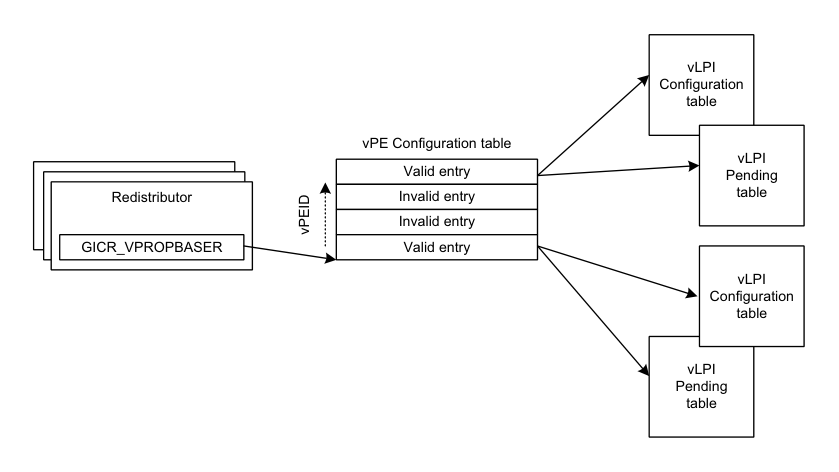
Image text
vLPI
Configuration
table
vPE Configuration table
vLPI
Valid entry Pending
Redistributor Invalid entry table
Invalid entry
GICR_VPROPBASER Valid entry
vLPI
Configuration
table
vLPI
Pending
table
vPEID
8.6.1 vPE Configuration table
The format of the vPE Configuration table is IMPLEMENTATION DEFINED. GICR_VPROPBASER.Z indicates whether the table contains all zeros. If the vPE Configuration table does not contain all zeros on initial allocation, the behavior is UNPREDICTABLE. When GICR_VPROPBASER.Z==0, the memory contents are not zero and contain valid data.
GICR_VPROPBASER.Valid indicates whether the vPE Configuration table is valid. If the vPE Configuration table is written by any agent other than the GIC when any Redistributor pointing at that table has GICR_VPROPBASER.Valid==1, the behavior is UNPREDICTABLE. When no Redistributor with GICR_VPROPBASER.Valid==1 has a pointer to a vPE Configuration Table, there are no cached copies of that vPE Configuration Table in any Redistributor.
When GICR_VPROPBASER.Valid is written from 1 to 0, all other read/write fields in the register become UNKNOWN. After writing GICR_VPROPBASER.Valid from 1 to 0, when GICR_CTLR.RWP==0, there are no further accesses to the vPE Configuration Table by that Redistributor.
GICR_VPROPBASER.Valid can be written from 1 to 0 while another Redistributor in the same CommonLPIAff group has GICR_CTLR.RWP==1 due a previous write of GICR_VPROPBASER.Valid from 1 to 0. If GICR_VPROPBASER.Valid is written from 0 to 1 when any Redistributor in the same CommonLPIAff group has GICR_CTLR.RWP==1 due a previous write of Valid from 1 to 0, the result is UNPREDICTABLE.
Writing GICR_VPROPBASER when GICR_CTLR.RWP==1 due a previous write of GICR_VPROPBASER.Valid from 1 to 0 on that Redistributor causes UNPREDICTABLE behavior.
Note The vPE Configuration Table is populated as a side effect of the VMAPP commands issued through the ITS. It is not intended to be accessed directly by software.
8.6.2 Residency and mapping restrictions
If the target Redistributor has GICR_VPROPBASER.Valid==0, a VMAPP command with V==1 has one of the following CONSTRAINED UNPREDICTABLE effects:
-
The mapping is discarded.
-
The mapping is made using the vPE Configuration Table from an UNKNOWN Redistributor with GICR_VPROPBASER.Valid==1.
If the target Redistributor has GICR_VPROPBASER.Valid==0, a VMOVP command has one of the following
CONSTRAINED UNPREDICTABLE effects:
-
The mapping is not moved.
-
The mapping is moved.
-
The mapping is discarded.
If the specified vPEID is beyond the range of the vPE Configuration table, a VMAPP command with V==1 has one of the following CONSTRAINED UNPREDICTABLE effects unless the command causes a command error:
-
The command is ignored.
-
The vPEID is treated as an UNKNOWN legal value.
If the specified vPEID is beyond the range of the vPE Configuration table, a VMOVP command has one of the following CONSTRAINED UNPREDICTABLE effects unless the command causes a command error:
-
The command is ignored.
-
The vPEID is treated as an UNKNOWN legal value.
If there are any ITS vPEID mappings that target the Redistributor, the effect of clearing GICR_VPROPBASER.Valid from 1 to 0 is UNPREDICTABLE.
Note Arm strongly recommends that all vPE mappings are removed from a Redistributor before clearing GICR_VPROPBASER.Valid.
If a vPEID is scheduled on multiple Redistributors at the same time, the effect is UNPREDICTABLE.
If a vPEID is scheduled on any Redistributor when there is no current ITS mapping for that vPEID, one of the following CONSTRAINED UNPREDICTABLE effects occurs:
-
GICR_VPENDBASER.vPEID is treated as having an UNKNOWN valid value for all purposes other than a direct read of the register.
-
GICR_VPENDBASER.Valid is treated as being set to 0 for all purposes other than a direct read of the register.
-
The vPEID is treated as mapped with an UNKNOWN configuration.
A vPEID can be scheduled on the Redistributor it is mapped to in the ITSs, or any other Redistributor within the same CommonLPIAff group. Scheduling a vPEID on a Redistributor in a different CommonLPIAff group has one of the following CONSTRAINED UNPREDICTABLE effects:
-
Pending interrupts are not delivered.
-
Interrupts are delivered that are not pending.
-
Incorrect configuration might be used for interrupts.
-
The guarantees on doorbell interrupts might not be respected.
If a vPEID is scheduled on any Redistributor when a VMOVP is issued for it, the result is UNPREDICTABLE.
8.7 Register based vLPI invalidation
Cached configuration data of a specific LPI can be invalidated using the GICR_INVLPIR register, or all LPIs using the GICR_INVALLR register, as follows:
-
Writing GICR_INVLPIR.V == 0 or GICR_INVALLR.V == 0 performs the invalidation on the physical INTID space.
-
Writing GICR_INVLPIR.V == 1 or GICR_INVALLR.V == 1 performs the invalidation on the virtual INTID space identified by the GICR_INVLPIR.vPEID or GICR_INVALLR.vPEID field, respectively.
When writing GICR_INVLPIR.V == 1, the invalidation operation has no effect when any of the following occur:
-
The GICR_INVLPIR.INTID field is outside the supported LPI range for that vPE.
-
The GICR_INVLPIR.INTID field is not an LPI.
Issuing a register-based invalidation operation for a vPEID not mapped to that Redistributor, or another Redistributor within the same CommonLPIAff group, has one of the following CONSTRAINED UNPREDICTABLE effects:
-
The operation is ignored.
-
The invalidation is completed affecting an UNKNOWN subset of the Redistributors.
-
The invalidation is completed affecting all Redistributors.
When writing GICR_INVLPIR or GICR_INVALLR, GICR_SYNCR.Busy tracks invalidates issued on the same Redistributor:
-
GICR_SYNCR.Busy == 1 until the invalidation completes.
-
When GICR_SYNCR.Busy == 0, the invalidate is complete and the effects of the invalidation are visible on all Redistributors, unless specified otherwise.
Writing GICR_INVLPIR or GICR_INVALLR when GICR_SYNCR.Busy==1 has one of the following CONSTRAINED UNPREDICTABLE effects:
-
The write is IGNORED.
-
The invalidate specified by the write is performed.
The effect of register based invalidate is only guaranteed to be visible to an ITS command after GICR_SYNCR records it as complete. Issuing an ITS command when there is an outstanding register based invalidate for an affected interrupt has one of the following CONSTRAINED UNPREDICTABLE effects:
-
The effect of the invalidate is applied before the ITS command.
-
The invalidate is ignored.
Issuing a register based invalidate for an interrupt when there is an outstanding ITS command that affects the interrupt has one of the following CONSTRAINED UNPREDICTABLE effects:
-
The effect of the invalidate is applied before the ITS command.
-
The effect of the invalidate is applied after the ITS command.
-
The invalidate is ignored.
The GICR_INVLPIR, GICR_INVALLR, and GICR_SYNCR registers are mandatory in GICv4.1.
8.8 Direct injection of vSGIs
A new mechanism is introduced to allow SGIs to be directly injected via the ITS. This mechanism still requires a trap to the hypervisor on the sending PE but removes the need for a trap to the hypervisor on the receiving PE(s). There are limitations on these controls:
-
The ITS controls must only be used on an ITS that has a mapping for that vPEID.
- Where multiple ITSs have a mapping for the vPEID, any ITS with a mapping may be used.
-
The Redistributor controls must only be used on the currently targeted Redistributor, or on a Redistributor within the same CommonLPIAff group. The vPEID does not need to be currently scheduled, only mapped.
- Where multiple ITSs have a mapping for the vPEID, any ITS with a mapping may be used.
Failure to follow these guidelines can lead to UNPREDICTABLE behaviors.
There is no control to query the current configuration of a vSGI. Software must keep its own copy of the current configuration of a vSGI to emulate reads of the GICR_IxxxR0 SGI configuration fields. vSGIs received through direct injection do not have an Active state.
8.8.1 Generating a vSGI
When GITS_CTLR.Enabled==1 and GITS_CTLR.Quiescent==0, a write to GITS_SGIR results in a virtual interrupt being generated with the vPEID and vINTID from the write. If the vPEID is not mapped on any ITS, the write is silently discarded. If the vPEID is not mapped on this ITS, but is mapped on a different ITS, it is CONSTRAINED UNPREDICTABLE whether the interrupt is delivered or discarded. Virtual SGIs have no priority shift.
8.8.2 Storing vSGI state and configuration
The last 128 bits of the IMPLEMENTATION DEFINED region in the Virtual LPI Pending Table are redefined for use storing SGI configuration and state. The format of this space is:
Table 8-1 Virtual LPI Pending Table
| 31 | 24 23 | 16 | 15 | 8 7 | 0 | Offset from start of Pending Table | |—|— Enable RES0 |—|—|— Pending Group |—|— +0x3F0 +0x3F4 | | PRI_7 | PRI_6 PRI_5 | PRI_4 | PRI_3 | PRI_2 PRI_1 | PRI_0 | +0x3F8 | | PRI_15 | PRI_14 PRI_13 | PRI_12 | PRI_11 | PRI_10 PRI_9 | PRI_8 | +0x3FC |
-
Pending[n]: The pending state of vSGI n:
-
0 - Not pending.
-
1 - Pending.
-
-
Enable[n]: The enable state of vSGI n:
-
0 - Disabled.
-
1 - Enabled.
-
-
Group[n]: The Group of vSGI n:
-
Group 0.
-
Group 1.
-
PRI_
8.8.3 Emulating GICR_I[C|S]PENDR0
Writing GICR_VSGIR queries the pending state of the virtual SGIs belonging to the specified vPE. GICR_VSGIPENDR.Busy determines when the query is complete, as follows:
-
GICR_VSGIPENDR.Busy == 1 until the query completes.
-
When GICR_VSGIPENDR.Busy == 0, the pending state of the vSGIs belonging to that vPE is reported in GICR_VSGIPENDR.Pending.
GICR_VSGIRPEND.Pending returns an UNKNOWN value in the following cases:
-
When GICR_VSGIPENDR.Busy == 1.
-
Writing a vPEID that is invalid or that is not mapped to this CommonLPIAff Redistributor group.
Writing GICR_VSGIR when GICR_VSGIPENDR.Busy == 1 has one of the following CONSTRAINED UNPREDICTABLE effects:
-
The write is ignored.
-
The write causes a fresh look up to occur.
The VSGI command allows writes to GICR_ISPENDR0 to be emulated. Writes to GICR_ISPENDR0 can be emulated using GITS_SGIR.
Chapter 9: Memory Partitioning and Monitoring
This chapter describes Memory Partitioning and Monitoring (MPAM) as it applies to the GICv3 architecture. It contains the following sections:
-
Overview.
-
MPAM and the Redistributors.
-
MPAM and the ITS.
-
GIC usage of MPAM.
-
GICv4.1 data structures and MPAM.
9.1 Overview
The GIC optionally supports MPAM. This support is limited to providing controls for software to set the Partition IDs (PARTIDs) that are used when the GIC accesses memory. A PARTID is an MPAM ID that indicates which memory system performance resource partition to use in the memory system components.
When GICD_CTLR.DS == 0, all PARTIDs that are used by the GIC are Non-secure MPAM IDs, and are communicated with the MPAM_NS indicator as true.
When GICD_CTLR.DS == 1, whether PARTIDs are Non-secure or Secure MPAM IDs is IMPLEMENTATION DEFINED.
Arm recommends that in a system that supports MPAM, software is able to control the PARTID that is used by the GIC when accessing data structures and the structures in memory.
See the following sections for more details on these structures:
-
LPI Configuration tables.
-
LPI Pending tables.
-
Virtual LPI Configuration tables and virtual LPI Pending tables.
-
The Device table.
-
The Interrupt translation table.
-
The Collection table.
-
The vPE table.
-
The ITS command interface.
9.2 MPAM and the Redistributors
GICR_TYPER.MPAM reports support for MPAM, and all Redistributors that are part of the same IRI report the same value of GICR_TYPER.MPAM.
GICR_MPAMIDR reports the PMG and PARTID sizes that are supported.
GICR_PARTIDR controls the PARTID and PMG that are used by the Redistributor.
Writing an out-of-range value to GICR_PARTIDR.PARTID results in CONSTRAINED UNPREDICTABLE behavior, and either:
-
The default values of PARTID and PMG are used, and returned on reads.
-
An UNKNOWN valid value is used, and returned on reads.
Writing an out-of-range value to GICR_PARTIDR.PMG results in CONSTRAINED UPREDICTABLE behavior, and either:
-
The default PMG value is used, and returned on reads.
-
An UNKNOWN valid value is used, and returned on reads.
A write to GICR_PARTIDR is only guaranteed to take effect the next time GICR_CTLR.Enable_LPIs is written from 0 to 1. An implementation must ensure that either the old value or the new value is used, and that at no point a partially updated value is used.
Note
Arm strongly recommends that software does not write GICR_PARTIDR while GICR_CTLR.Enable_LPIs == 1, because of the uncertainty of when the change takes effect.
For Redistributors that are required to share an LPI Configuration table, it is IMPLEMENTATION DEFINED whether GICR_PARTIDR accesses common state. GICR_TYPER.CommonLPIAff indicates which Redistributors are required to share an LPI Configuration table.
When GICR_TYPER.MPAM == 1, all accesses by the Redistributor to the following data structures use the PARTID and PMG values that are specified in GICR_PARTIDR:
-
LPI Pending table.
-
LPI Configuration table.
-
Virtual LPI Pending table.
-
Virtual LPI Configuration table.
9.3 MPAM and the ITS
GITS_TYPER.MPAM reports support for MPAM, and all ITSs that are part of the same IRI report the same value of GITS_TYPER.MPAM.
GITS_MPAMIDR reports the PMG and PARTID sizes that are supported.
GITS_PARTIDR controls the PARTID and PMG that are used by the ITS.
Writing an out-of-range value to GITS_PARTIDR.PARTID results in CONSTRAINED UNPREDICTABLE behavior, and either:
-
The default values of PARTID and PMG are used, and returned on reads.
-
An UNKNOWN valid value is used, and returned on reads.
Writing an out-of-range value to GITS_PARTIDR.PMG results in CONSTRAINED UPREDICTABLE behavior, and either:
-
The default PMG value is used, and returned on reads.
-
An UNKNOWN valid value is used, and returned on reads.
A write to GITS_PARTIDR is only guaranteed to take effect the next time GITS_CTLR.Enable is written from 0 to 1. An implementation must ensure that either the old value or the new value is used, and that at no point a partially updated value is used.
Note
Arm strongly recommends that software does not write GITS_PARTIDR while GITS_CTLR.Enable == 1, because of the uncertainty of when the change takes effect.
When GITS_TYPER.MPAM == 1, all accesses by the Redistributor to the following data structures use PARTID and PMG values that are specified in GITS_PARTIDR:
-
Device table.
-
Interruption Translation table.
-
Collection table.
-
Virtual PE table.
-
Command queue.
9.4 GIC usage of MPAM
This extension is limited to providing a mechanism for software to specify the PARTIDs that are used by the GIC when accessing memory.
Any support for using PARTIDs to internally partition resources or monitor performance is IMPLEMENTATION DEFINED.
Where an implementation provides such support, Arm expects it to do so in accordance with what is described in the Arm[®] Architecture Reference Manual Supplement, Memory System Resource Partitioning and Monitoring (MPAM), for Armv8-A .
9.5 GICv4.1 data structures and MPAM
When MPAM is supported, and GITS_TYPER.SVPET==0, accesses to the vPE Configuration Table use the PARTID and PMG values from GICR_PARTIDR.
When MPAM is supported, and GITS_TYPER.SVPET!=0, accesses to the vPE Configuration Table use the PARTID and PMG values from:
Table 9-1 PARTID usage in GICv4.1 |—|—|—| | GICR_VPROPBASER.Valid | GITS_CTLR.Enabled | MPAM information from: | | x | 1 | GITS_PARTIDR | | 0 | 1 | GITS_PARTIDR | | 1 | 1 | GICR_PARTIDRorGITS_PARTIDR | | 1 | 0 | GICR_PARTIDR |
When the vPE Configuration Table is shared between the Redistributor(s) and ITS(s), either the Redistributors or ITS PARTID and PMG values can be used to access the table, and this can vary depending on the cause of the access.
Chapter 10: Connecting to Armv8-R AArch64 PEs
This chapter describes the requirements for connecting a GIC to PEs that implement Armv8-R AArch64: • Armv8-R AArch64 CPU interface requirements .
Collectively, these restrictions are referred to as GICv3.2.
10.1 Armv8-R AArch64 CPU interface requirements
10.1.1 Impact to legacy mode
Legacy operation is not supported. When GIC is used with Armv8-R AArch64 PEs, the ICC_SRE_ELx.SRE bits are RES1.
10.1.2 GICv3.1 extended INTID range support
When GIC v3.1 is used with Armv8-R AArch64 PEs, ICC_CTLR_EL1.ExtRange==0 is deprecated.
Note Arm recommends that Armv8-R AArch64 PEs report ICC_CTLR_EL1.ExtRange==1, indicating that the GICv3.1 extended SPI and PPI ranges are supported.
10.1.3 LPI support
Armv8-R AArch64 PEs support LPIs.
GIC IRIs that support LPIs can be connected to PEs that implement Armv8-R AArch64.
10.1.4 Local SError generation support
Armv8-R AArch64 does not support local SError generation by the CPU interface. When GIC is used with Armv8-R AArch64 PEs, the ICH_VTR_EL2.SEIS and ICC_CTLR_EL1.SEIS are RES0.
10.1.5 Virtualization support
When GIC is used with Armv8-R AArch64 PEs, the ICH_VTR_EL2.TDS is RES1, indicating that ICH_HCR_EL2.TDIR is supported.
Chapter 11: Power Management
-
This chapter describes power management. It contains the following section:
-
Power management .
11.1 Power management
In an implementation compliant with the GICv3 architecture, the CPU interface and the PE must be in the same power domain, but this does not have to be the same power domain as that within which the associated Redistributor is located. This means that it is possible to have a situation where the PE and its CPU interface are powered down, and the Redistributor, Distributor, and ITS, are powered up. In this situation, the GIC architecture supports the use of interrupts targeted at the PE to signal a powerup event to the PE and CPU interface.
Note Arm strongly recommends that the GIC is not configured in such a way that an interrupt can cause wake-up of a particular PE, if on waking software on that PE cannot handle the interrupt.
GICv3 provides power management to control this situation, because the architecture is designed to allow the Redistributors designed by one organization to be used with PEs and CPU interfaces that have been designed by a different organization.
All other aspects of power management for the GIC are IMPLEMENTATION DEFINED.
Before powering down the CPU interface and the PE when the Redistributor is powered up, software must put the interface between the CPU interface and the Redistributor into the quiescent state or the system will become UNPREDICTABLE. The transition to the quiescent state is initiated by setting GICR_WAKER.ProcessorSleep to 1. When the interface is quiescent, GICR_WAKER.ChildrenAsleep is also set to 1.
GICR_WAKER.ProcessorSleep == 1 has the following effects:
-
The Redistributor does not forward any interrupts for the PE to the CPU interface. If there is a pending interrupt for the PE that would otherwise be forwarded to the PE, a hardware signal, WakeRequest , is asserted to indicate that the PE is to have its power restored. In a GICv4 implementation, this applies to virtual LPIs in addition to any other interrupts.
-
The Distributor does not select this PE as a candidate for selection for a 1 of N interrupt, unless GICD_CTLR.E1NWF == 1, and the PE has been selected by an IMPLEMENTATION DEFINED mechanism:
- For a 1 of N interrupt that causes wake-up, the GIC is not required to select a new target PE if the PE that received the WakeRequest does not handle the interrupt on waking.
When the interface between the Redistributor and the CPU interface is in a quiescent state, the following architectural state of the CPU interface can be saved as part of saving the state within the power domain of the CPU interface and the PE:
-
The CPU interface state related to physical interrupts of the connected PE.
-
The CPU interface state related to virtual interrupts that is part of the vPE that is scheduled on the associated PE.
Setting GICR_WAKER.ProcessorSleep to 1 when the physical group enables in the CPU interface are set to 1 results in UNPREDICTABLE behavior.
When GICR_WAKER.ProcessorSleep == 1 or GICR_WAKER.ChildrenAsleep == 1 then a write to any GICC_, GICV_, GICH_, ICC_, ICV_, or ICH_ registers, other than those in the following list, is unpredictable:
-
ICC_SRE_EL1.
-
ICC_SRE_EL2.
-
ICC_SRE_EL3.
Chapter 12: Programmers’ Model
This chapter provides information about the GIC register interfaces and describes all of the GIC registers. It contains the following sections:
-
About the programmers’ model.
-
AArch64 System register descriptions.
-
AArch64 System register descriptions of the virtual registers.
-
AArch64 virtualization control System registers.
-
AArch32 System register descriptions.
-
AArch32 System register descriptions of the virtual registers.
-
AArch32 virtualization control System registers.
-
The GIC Distributor register map.
-
The GIC Distributor register descriptions.
-
The GIC Redistributor register map.
-
The GIC Redistributor register descriptions.
-
The GIC CPU interface register map.
-
The GIC CPU interface register descriptions.
-
The GIC virtual CPU interface register map.
-
The GIC virtual CPU interface register descriptions.
-
The GIC virtual interface control register map.
-
The GIC virtual interface control register descriptions.
-
The ITS register map.
-
The ITS register descriptions.
-
Pseudocode.
12.1 About the programmers’ model
The GIC is partitioned into several logical components, as defined in Chapter 3 GIC Partitioning , and each component supports one or more programming interfaces. Software uses these programming interfaces to access the programmers’ model and control the GIC. The interfaces are either memory-mapped or support System register accesses as follows:
-
The Distributor, Redistributor, and ITS programming interfaces are always memory-mapped.
-
The CPU interfaces for physical and virtual interrupt handling, and the virtual machine control interface used by the hypervisor use:
-
System register interfaces for the operation of GICv3 and GICv4.
-
Memory-mapped interfaces for legacy operation.
Note Support for legacy operation is optional. Implementations are allowed to support legacy operation for virtual interrupts only, meaning that the GICV_* registers are the only memory-mapped CPU interface registers that are provided. In these implementations, GICC_* registers and GICH_* registers are not provided. GICC_* and GICH_* registers are only required to support legacy operation by physical interrupts.
When accessing a System register, the register content accessed depends on:
-
The Exception level at which the PE is executing.
-
Whether the access is Secure or Non-secure.
-
For a Non-secure access at EL1, whether the Exception level is configured by HCR_EL2 when executing in AArch64 state, or by HCR when executing in AArch32 state, to handle virtual or physical interrupts.
12.1.1 GIC register names
All of the GIC registers have names that provide a short mnemonic for the function of the register:
-
Memory-mapped registers are prefixed by one of the following:
- GICC, to indicate a CPU interface register. - GICD, to indicate a Distributor register.-
GICH, to indicate a virtual interface control register, typically accessed by a hypervisor.
-
GICR, to indicate a Redistributor register.
-
GICV, to indicate a virtual CPU interface register.
-
GITS, to indicate an ITS register.
-
-
System registers are prefixed by:
- ICC, to indicate a physical GIC CPU interface System register.-
ICV, to indicate a virtual GIC CPU interface System register.
-
ICH, to indicate a virtual interface control System register.
-
-
The remaining letters are a mnemonic for the register, for example the GIC Distributor Control Register is called GICD_CTLR.
Figure 12-1 shows the interfaces that the programmer can use for the different logical components when affinity routing and System register access are enabled for all Exception levels.
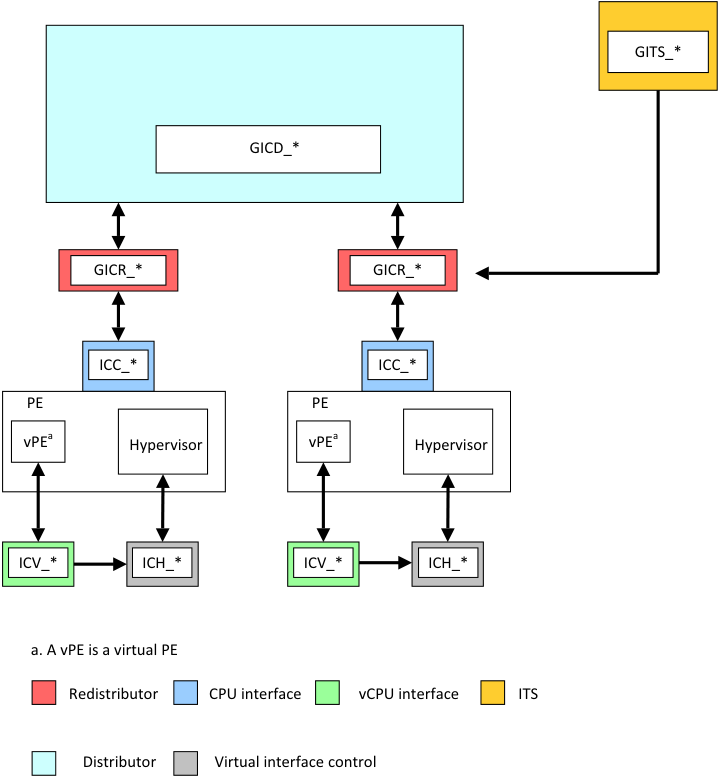
Image text
GITS_
GICD_
GICR_* GICR_
ICC_ ICC_
PE PE
vPE [a] Hypervisor vPE [a] Hypervisor
ICV_ ICH_* ICV_* ICH_*
a. A vPE is a virtual PE
Redistributor CPU interface vCPU interface ITS
Distributor Virtual interface control
12.1.2 Relation between System registers and memory-mapped registers
The GIC architecture permits, but does not require, that the same registers can be shared between memory-mapped registers and the equivalent System registers. This means that if the memory-mapped registers have been accessed while ICC_SRE_ELx.SRE == 0, the System registers might be modified. Therefore, Arm recommends that software only relies on the reset values of the System registers if there has been no use of the GIC functionality while the memory-mapped registers are in use, otherwise Arm recommends that the values are treated as UNKNOWN. Table 12-1 shows the registers that are shared between the memory-mapped registers and the System registers.
Table 12-1 Relation between System registers and memory-mapped registers
| System registersa AArch64 | Memory-mapped CPU interface registers AArch32 | Memory-mapped virtual CPU interface registers |
|---|---|---|
| ICC_AP0R | ICC_AP0R | GICV_APR |
| ICC_BPR0_EL1 | ICC_BPR0 GICC_BPR,GICC_ABPRbc ICC_BPR1 | GICV_BPR |
| ICC_BPR1_EL1 | GICV_ABPR | |
| ICC_CTLR_EL1 ICC_CTLR_EL3 | ICC_CTLR GICC_CTLR ICC_MCTLR | GICV_CTLR |
| ICC_DIR_EL1 | ICC_DIR GICC_DIR | GICV_DIR |
| ICC_EOIR0_EL1 | ICC_EOIR0 GICC_EOIR,GICC_AEOIR ICC_EOIR1 | GICV_EOIR |
| ICC_EOIR1_EL1 | GICV_AEOIR | |
| ICC_HPPIR0_EL1 | ICC_HPPIR0 GICC_HPPIR,GICC_AHPPIR ICC_HPPIR1 | GICV_HPPIR |
| ICC_HPPIR1_EL1 | GICV_AHPPIR | |
| ICC_IAR0_EL1 | ICC_IAR0 GICC_IAR,GICC_AIARd ICC_IAR0 | GICV_IAR |
| ICC_IAR1_EL1 | GICV_AIAR | |
| ICC_IGRPEN0_EL1 ICC_IGRPEN1_EL1 ICC_IGRPEN1_EL3 | ICC_IGRPEN0 GICC_CTLR ICC_IGRPEN1 ICC_MGRPEN1 | GICV_CTLR |
| ICC_PMR_EL1 | ICC_PMR GICC_PMR | GICV_PMR |
| ICC_RPR_EL1 | ICC_RPR GICC_RPR | GICV_RPR |
| ICH_AP0R | ICH_AP0R | - |
| ICH_AP1R | - | |
| ICH_EISR_EL2 | ICH_EISR GICH_EISR | - |
| ICH_ELRSR_EL2 | ICH_ELRSR GICH_ELRSR | - |
| ICH_HCR_EL2 | ICH_HCR GICH_HCR | - |
| ICH_LR | ICH_LR | - |
| - | ||
| ICH_MISR_EL2 | ICH_MISR GICH_MISR | - |
| ICH_VMCR_EL2 | ICH_VMCR GICH_VMCR | - |
| ICH_VTR_EL2 | ICH_VTR GICH_VTR | - |
-
a. There are also System registers prefixed with ICV, rather than ICC, and these are the virtual GIC CPU interface System registers, see AArch64 System register descriptions of the virtual registers and AArch32 System register descriptions of the virtual registers.
-
b. This register is an alias of the Non-secure copy of GICC_BPR.
-
c. If ICC_CTLR_EL3.CBPR_EL1NS == 1, Secure accesses to this register access (and might modify) ICC_BPR0_EL1.
-
d. In GIC implementations that support two Security states, this register is an alias of the Non-secure view of GICC_IAR.
12.1.3 GIC memory-mapped register access
In any system, access to the following registers must be supported:
-
Single copy atomic 32-bit accesses to:
- All 32-bit GICC_, GICV_, GICD_, GICH_, GITS_, and GICR_ registers.
-
Single copy atomic 64-bit accesses to:
-
All 64-bit GITS_* registers.
-
— All 64-bit GICD_* registers.
-
— All 64-bit GICR_* registers.
-
-
Byte accesses to: — GICD_IPRIORITYR
. -
GICD_ITARGETSR
. -
GICD_SPENDSGIR
. -
— GICD_CPENDSGIR
. -
GICR_IPRIORITYR
.
-
In addition, in system where one or more PE supports AArch32:
-
Single copy atomic 32-bit accesses to:
- All 64-bit GICD_, GICR_, and GITS_* registers, including independent access to the upper 32-bits and the lower 32-bits of the register. This does not apply to registers that are specifically marked as being 64-bit accessible only.
Arm does not expect the following registers to be accessed directly by software, but single-copy atomic 16-bit and 32-bit accesses to these registers must be supported:
-
GITS_TRANSLATER.
-
GICD_SETSPI_NSR.
-
GICD_CLRSPI_NSR.
-
GICD_SETSPI_SR.
-
GICD_CLRSPI_SR.
All other accesses to these registers result in UNPREDICTABLE behavior.
In the GIC architecture, all registers that are doubleword-accessible, halfword-accessible, or byte-accessible use a little-endian memory order model.
The following accesses are not supported:
-
Byte access to registers other than those specifically listed in this section.
-
Unaligned word accesses. These accesses are not word single-copy atomic.
-
Unaligned doubleword accesses. These accesses are not doubleword single-copy atomic.
-
Word accesses for registers marked as requiring a 64-bit access.
-
Doubleword accesses, other than those specifically listed in this section.
-
Quadword or higher.
-
Exclusive accesses.
For each of these access types, it is UNPREDICTABLE whether:
-
The access generates an external abort or not.
-
The defined side-effects of a read occur or not. A read returns UNKNOWN data.
-
A write is ignored or sets the accessed register or registers to UNKNOWN values.
For memory-mapped accesses by a PE that complies with the Arm architecture, the single-copy atomicity rules for the instruction, the type of instruction, and the type of memory accessed, determine the size of the access made by the instruction. Example 12-1 shows this.
Example 12-1 Access sizes for memory-mapped accesses
Two Load Doubleword instructions made to consecutive doubleword-aligned locations generate a pair of single-copy atomic doubleword reads. However, if the accesses are made to Normal memory or Device-GRE memory they might appear as a single quadword access that is not supported by the peripheral.
Armv8 does not require the size of each element accessed by a multi-register load or store instruction to be identifiable by the memory system beyond the PE. Any memory-mapped access to a GIC is defined to be beyond the PE.
Software must use a Device-nGRE or stronger memory-type, and use only single register load and store instructions, to create memory accesses that are supported by the peripheral.
Reads and writes of the memory-mapped registers complete in the order in which they arrive at the GIC. For access to different register locations, software must create this order by:
-
Marking the memory as Device-nGnRnE or Device-nGnRE.
-
Using the appropriate memory barriers.
Software must be able to guarantee completion of a write, for example by:
-
Marking the memory as Device-nGnRnE and executing a DSB barrier, if the system supports this property.
-
Reading back the value written.
For more information on endianness, memory ordering, and barrier instructions, see Arm[®] Architecture Reference Manual, Armv8, for Armv8-A architecture profile.
The access type definitions for the memory-mapped register interface are:
RW Read and write. RO Read only. Writes are ignored. WO Write only. Reads return an UNKNOWN value.
12.1.4 Access to memory-mapped registers when System register access is enabled
Because memory-mapped accesses and System register accesses might not access the same state, and are not guaranteed to be synchronized when System registers access is enabled for a particular Exception level and Security state, Arm recommends that the System registers be used instead of the memory-mapped registers that provide the same functionality.
In implementations that include the GICC_* registers, and where the Secure copy of ICC_SRE_EL1.SRE is programmable, the following state must be shared between System register access and memory-mapped access to ensure the correct operation of preemption:
-
GICC_PMR and ICC_PMR_EL1 or ICC_PMR must access the same state.
-
GICC_APR
and ICC_AP0R _EL1 must access the same state. -
GICC_NSAPR
and ICC_AP1R _EL1(NS) must access the same state. -
GICC_CTLR.CBPR and ICC_CTLR_EL3(NS).CBPR must access the same state.
-
Secure accesses to GICC_BPR and ICC_BPR0_EL1 must access the same state when GICC_CTLR.CBPR == 0.
-
Secure accesses to GICC_ABPR and ICC_BPR1_EL1 must access the same state when GICC_CTLR.CBPR == 0.
Note
-
Software must follow the rules specified in GIC System register access when changing the setting of the SRE fields.
-
Relation between System registers and memory-mapped registers specifies the relationship between memory-mapped registers and System registers. State can only be shared between registers that perform the same function, and the registers listed in Table 12-1 might share state.
When changing from a state where the registers are required to access the same state to a state where the registers are not required to access the same state, or when changing from a state where the registers are not required to access the same state to a state where the registers are required to access the same state, the content of the registers becomes UNKNOWN.
Note The priority bits implemented for memory-mapped and System register state must be the same, as must the minimum value of the Binary Point Register for Group 0 interrupts for both Secure and Non-secure views.
Accesses to the GICC_* registers might be affected by whether System register access is enabled or not, depending on the implementation:
- If the Secure copy of ICC_SRE_EL1.SRE == 1, then the GICC_* registers might not be accessible or might be RAZ/WI.
Note
When EL3 is configured to use AArch32 state, Secure EL1 is not accessible but software must still set the Secure copy of ICC_SRE.SRE to 1, to enable support for Secure Group 1 interrupts, otherwise the system is UNPREDICTABLE.
-
If ICC_SRE_EL2.SRE ==1, then the GICH_* registers might not be accessible or might be RAZ/WI.
-
If the Non-secure copy of ICC_SRE_EL1.SRE == 1, then the GICV_* registers might not be accessible or might be RAZ/WI.
Note In implementations where the Non-secure copy of ICC_SRE_EL1.SRE is programmable, that is, it is not RAO/WI, the GICV_* register interface must still be provided.
An implementation might be able to detect accesses to memory-mapped registers that must not be accessed because an SRE bit is 1, and report them in an IMPLEMENTATION DEFINED manner.
12.1.5 Execution state
The Armv8-A architecture has two Execution states:
-
AArch64 state.
-
AArch32 state.
To see the mapping between the AArch64 System registers and the AArch32 System registers, see:
-
Table 12-3.
-
Table 12-4.
12.1.6 Observability of the effects of accesses to the GIC registers
The PE and CPU interface logic must ensure that:
- Writes to ICC_PMR_EL1 are self-synchronizing.
Note This ensures that no interrupts with a priority lower than the priority value in ICC_PMR_EL1 are taken after a write to ICC_PMR_EL1 is architecturally executed.
- Reads of ICC_IAR0_EL1 and ICC_IAR1_EL1 are self-synchronizing when interrupts are masked by the PE, that is when PSTATE.F == 1, for reads of ICC_IAR0_EL1, and when PSTATE.I == 1, for reads of ICC_IAR1_EL1.
Note This ensures that the effect of activating an interrupt on the signaling of an interrupt exception is observed when a read of ICC_IAR0_EL1 and ICC_IAR1_EL1 is architecturally executed. This means that no spurious interrupt exception occurs if interrupts are unmasked by an instruction immediately following the read.
-
Instructions that change the current Exception level from EL3 to a lower Exception level, for example the ERET instruction, must be synchronized with any corresponding change in the allocation of interrupts as FIQs and IRQs, so that no spurious FIQ is taken after the architectural execution of the instruction, see Interrupt assignment to IRQ and FIQ signals.
-
Architectural execution of a DSB instruction guarantees that
-
The last value written to ICC_PMR_EL1 or GICC_PMR is observed by the associated Redistributor. PMR values are only observable by the Redistributor when ICC_CTLR_ELx.PMHE==1, and observation by the Redistributor does not affect masking of interrupts within the CPU interface.
-
The last value written to ICC_SGI0R_EL1 or ICC_SGI1R_EL1 is observed by the associated Redistributor.
-
The last value written to ICC_ASGI1R_EL1 is observed by the associated Redistributor.
-
The last value written to ICC_IGRPEN0_EL1, ICC_IGRPEN1_EL1, ICC_IGRPEN1_EL3 or GICC_CTLR.{EnableGrp0, EnableGrp1}is observed by the associated Redistributor.
-
The last value written to ICH_VMCR_EL2.{VENG0, VENG1}, or GICV_CTLR.{EnableGrp0, EnableGrp1} is observed by the associated Redistributor.
-
-
The last SPI INTID read from ICC_IAR0_EL1, ICC_IAR1_EL1, GICC_IAR or GICC_AIAR is observed by the Distributor and by accesses from any PE to the Distributor.
-
The last SGI, PPI or LPI INTID read from ICC_IAR0_EL1, ICC_IAR1_EL1, GICC_IAR or GICC_AIAR is observed by the associated Redistributor and by accesses from the PE to the associated Redistributor.
-
The last vLPI INTID read from ICV_IAR1_EL1, where that vLPI was received from a direct injection, is observed by the associated Redistributor.
-
The last Deactivate command for an SPI generated by a write to ICC_EOIR0_EL1, ICC_EOIR1_EL1, GICC_AEOIR, GICC_EOIR, ICC_DIR_EL1 or GICC_DIR is observed by the Distributor and by accesses from any PE to the Distributor.
-
The last Deactivate command for an SGI or PPI generated by a write to ICC_EOIR0_EL1, ICC_EOIR1_EL1, GICC_AEOIR, GICC_EOIR, ICC_DIR_EL1 or GICC_DIR is observed by the Redistributor and by accesses from any PE to the Redistributor.
-
The last Deactivate command for a physical PPI, SGI, or SPI generated by a write to ICV_EOIR0_EL1, ICV_EOIR1_EL1, GICV_AEOIR, GICV_EOIR, ICV_DIR_EL1, or GICV_DIR is observed by the Redistributor and by accesses from any PE to the Redistributor.
In all cases in this section where a DSB is referred to, this refers to a DSB whose required access type is both loads and stores with any Shareability attribute.
For more information about the encoding of the DSB instruction, see the Arm[®] Architecture Reference Manual, Armv8, for Armv8-A architecture profile .
Note An ISB or other context synchronization operation must precede the DSB to ensure visibility of System register writes.
12.1.7 GIC System register access
The GIC System register interface is managed by Exception level, using the following AArch64 System registers:
-
ICC_SRE_EL3, if EL3 is implemented.
-
ICC_SRE_EL2, if EL2 is implemented.
-
ICC_SRE_EL1.
Table 12-2 shows the permitted ICC_SRE_ELx.SRE settings.
Table 12-2 Permitted ICC_SRE_ELx.SRE settings
| ICC_SRE_EL1(S) ICC_SRE_EL1(NS) ICC_SRE_EL2 ICC_SRE_EL3 | Notes |
|---|---|
| 0 0 0 0 | Legacy, seeChapter 14_Legacy_ Operation and Asymmetric Configurations |
| 0 0 0 1 | Supported only when EL3 is using AArch64 |
| 0 0 1 1 | Supported only when EL3 is using AArch64 and virtual interrupts are enabled |
| 0 1 1 1 | Supported only when EL3 is using AArch64 |
| 1 0 1 1 | Supported only when HCR_EL2.FMO==1 &&HCR_EL2.IMO==1&& HCR_EL2.AMO==1 Note An implementation is permitted but not required to support this setting when HCR_EL2.FMO==1&& HCR_EL2.IMO==1. |
| 1 1 1 1 | Fully supported System register access |
Note The information in Table 12-2 applies to implementations that support both EL2 and EL3.
All combinations of ICC_SRE_ELx.SRE settings not listed in Table 12-2 result in UNPREDICTABLE behavior.
All settings other than ICC_SRE_ELx.SRE == 1 are deprecated.
Note
-
When HCR_EL2 is configured so that virtualization at EL1 is enabled, it is IMPLEMENTATION DEFINED whether a Non-secure access to ICC_SRE_EL1.SRE or ICC_SRE.SRE is programmable to support a legacy VM.
-
Arm expects that when ICC_SRE_EL3.SRE == 1 and ICC_SRE_EL1(S).SRE == 0, then ICC_CTLR_EL3.RM == 1.
The following changes to ICC_SRE_ELx result in UNPREDICTABLE behavior:
-
Changing the value of ICC_SRE_EL3.SRE from 1 to 0.
-
Changing the value of ICC_SRE_EL2.SRE from 1 to 0.
-
Changing the value of ICC_SRE_EL1(S).SRE from 1 to 0.
Note ICC_SRE_EL1(NS) can be changed from 1 to 0 to allow different VMs to have different ICC_SRE_EL1 values.
Each ICC_SRE_ELx register listed in this section provides:
-
An SRE bit to enable the ICC_* System register interface at that Exception level. For EL2 and EL3, the SRE bit also enables access to all ICH_* registers.
-
DIB and DFB bits to support interrupt bypass for the Exception level hierarchy. For more information about bypass, see Interrupt bypass support.
In addition:
-
ICC_SRE_EL3.Enable controls EL1 access to ICC_SRE_EL1, and EL2 access to ICC_SRE_EL1 and ICC_SRE_EL2.
-
ICC_SRE_EL2.Enable controls Non-secure EL1 accesses to ICC_SRE_EL1 if EL3 is not present or ICC_SRE_EL3.Enable == 1.
Note The ICC_SRE_ELx register associated with the highest implemented Exception level is always accessible to allow software executing at that Exception level to configure the System register at different Exception levels.
The System register interface can be used for execution in both AArch32 state and AArch64 state.
For AArch32 state, accesses to GIC registers that are visible in the System register interface use the following instructions:
-
The MRC instruction for 32-bit read accesses.
-
The MCR instruction for32-bit write accesses.
-
The MCRR instruction for 64-bit write accesses to ICC_SGI0R, ICC_SGI1R and ICC_ASGI1R.
See the Arm[®] Architecture Reference Manual, Armv8, for Armv8-A architecture profile for information about the form of the MRC, MCR, and MCRR instructions.
System registers support 32-bit or 64-bit accesses. See the individual register description for the associated access size.
The access type definitions for the System register interface are:
RW Read and write. RO Read only. Writes result in an UNDEFINED exception. WO Write only. Reads result in an UNDEFINED exception.
Note For more information about UNDEFINED exceptions, see Arm[®] Architecture Reference Manual, Armv8, for Armv8-A architecture profile . Table 12-3 shows the AArch64 and AArch32 register mappings for System register accesses by the GIC CPU interface.
Table 12-3 System register accesses for GIC CPU interface registers
| Name of System register accessed | Name of System register accessed |
|---|---|
| AArch64 | AArch32 |
| ICC_IAR0_EL1a | ICC_IAR0 |
| ICC_IAR1_EL1a | ICC_IAR1 |
| ICC_EOIR0_EL1a | ICC_EOIR0 |
| ICC_EOIR1_EL1a | ICC_EOIR1 |
| ICC_HPPIR0_EL1a | ICC_HPPIR0 |
| ICC_HPPIR1_EL1a | ICC_HPPIR1 |
| ICC_BPR0_EL1a | ICC_BPR0 |
| ICC_BPR1_EL1a | ICC_BPR1 |
| ICC_DIR_EL1a | ICC_DIR |
| ICC_PMR_EL1 | ICC_PMR |
| ICC_RPR_EL1 | ICC_RPR |
| ICC_AP0R | ICC_AP0R |
| ICC_AP1R | ICC_AP1R |
| ICC_CTLR_EL1 | ICC_CTLR |
| ICC_CTLR_EL3 | ICC_MCTLR |
| ICC_IGRPEN0_EL1 | ICC_IGRPEN0 |
| ICC_IGRPEN1_EL1 | ICC_IGRPEN1 |
| ICC_IGRPEN1_EL3 | ICC_MGRPEN1 |
| ICC_SGI1R_EL1 | ICC_SGI1R |
| ICC_ASGI1R_EL1 | ICC_ASGI1R |
| ICC_SGI0R_EL1 | ICC_SGI0R |
| ICC_SRE_EL1 | ICC_SRE |
| ICC_SRE_EL2 | ICC_HSRE |
| ICC_SRE_EL3 | ICC_MSRE |
a. In addition to ICC_SRE_EL*.SRE, ICC_SRE.SRE, ICC_HSRE.SRE, and ICC_MSRE.SRE, SCR_EL3 and HCR_EL2 control accessibility to these registers.
The GIC virtual interface control registers are accessible when ICC_SRE_EL2.SRE == 1. Table 12-4 shows the AArch64 and AArch32 System register mappings for the GIC virtual interface control registers.
Table 12-4 System register mappings for GIC virtual interface control registers
| Name of System register | accessed |
|---|---|
| AArch64 | AArch32 |
| ICH_HCR_EL2 | ICH_HCR |
| ICH_VTR_EL2 | ICH_VTR |
| ICH_MISR_EL2 | ICH_MISR |
| ICH_EISR_EL2 | ICH_EISR |
| ICH_ELRSR_EL2 | ICH_ELRSR |
| ICH_AP0R | ICH_AP0R |
| ICH_AP1R | ICH_AP1R |
| ICH_LR | ICH_LRC |
| ICH_LR | ICH_LR |
| ICH_VMCR_EL2 | ICH_VMCR |
| a. n = 0-3 | |
| b. n = 0-15. |
AArch64 System register access instruction encodings
Table 12-5 shows the format of the A64 MSR and MRS instructions to access the physical and virtual CPU interface.
Table 12-5 Mapping of MSR and MRS to physical and virtual CPU interface registers, AArch64 state
| System register | Access | opc0 | opc1 | CRn | CRm | opc2 |
|---|---|---|---|---|---|---|
| ICC_AP0R | RW | 3 | 0 | c12 | c8 | 4-7 |
| ICC_AP1R | RW | 3 | 0 | c12 | c9 | 0-3 |
| ICC_ASGI1R_EL1 | WO | 3 | 0 | c12 | c11 | 6 |
| ICC_BPR0_EL1 | RW | 3 | 0 | c12 | c8 | 3 |
| ICC_BPR1_EL1b | RW | 3 | 0 | c12 | c12 | 3 |
| ICC_CTLR_EL1b | RW | 3 | 0 | c12 | c12 | 4 |
| ICC_CTLR_EL3 | RW | 3 | 6 | c12 | c12 | 4 |
| ICC_DIR_EL1 | WO | 3 | 0 | c12 | c11 | 1 |
| ICC_EOIR0_EL1 | WO | 3 | 0 | c12 | c8 | 1 |
| ICC_EOIR1_EL1 | WO | 3 | 0 | c12 | c12 | 1 |
| ICC_HPPIR0_EL1 | RO | 3 | 0 | c12 | c8 | 2 |
| ICC_HPPIR1_EL1 | RO | 3 | 0 | c12 | c12 | 2 |
| Table 12-5 Mapping of MSR and MRS to physical and virtual CPU interface registers, AArch64 state (continued) |
| System register | Access | opc0 | opc1 | CRn | CRm | opc2 |
|---|---|---|---|---|---|---|
| ICC_IAR0_EL1 | RO | 3 | 0 | c12 | c8 | 0 |
| ICC_IAR1_EL1 | RO | 3 | 0 | c12 | c12 | 0 |
| ICC_IGRPEN0_EL1 | RW | 3 | 0 | c12 | c12 | 6 |
| ICC_IGRPEN1_EL1b | RW | 3 | 0 | c12 | c12 | 7 |
| ICC_IGRPEN1_EL3 | RW | 3 | 6 | c12 | c12 | 7 |
| ICC_PMR_EL1 | RW | 3 | 0 | c4 | c6 | 0 |
| ICC_RPR_EL1 | RO | 3 | 0 | c12 | c11 | 3 |
| ICC_SGI0R_EL1 | WO | 3 | 0 | c12 | c11 | 7 |
| ICC_SGI1R_EL1 | WO | 3 | 0 | c12 | c11 | 5 |
| ICC_SRE_EL1b | RW | 3 | 0 | c12 | c12 | 5 |
| ICC_SRE_EL2 | RW | 3 | 4 | c12 | c9 | 5 |
| ICC_SRE_EL3 a. n = 0-3. | RW | 3 | 6 | c12 | c12 | 5 |
| b. There is a Secure | copy and a Non-secure copy of this | register. |
Table 12-6 shows the format of the A64 MSR and MRS instructions that access the virtual interface control registers.
Table 12-6 Mapping of MSR and MRS to virtual interface control registers, AArch64 state
| System register | Access | opc0 | opc1 | CRn | CRm | opc2 |
|---|---|---|---|---|---|---|
| ICH_AP0R | RW | 3 | 4 | c12 | c8 | 0-3 |
| ICH_AP1R | RW | 3 | 4 | c12 | c9 | 0-3 |
| ICH_HCR_EL2 | RW | 3 | 4 | c12 | c11 | 0 |
| ICH_VTR_EL2 | RO | 3 | 4 | c12 | c11 | 1 |
| ICH_MISR_EL2 | RO | 3 | 4 | c12 | c11 | 2 |
| ICH_EISR_EL2 | RO | 3 | 4 | c12 | c11 | 3 |
| ICH_ELRSR_EL2 | RO | 3 | 4 | c12 | c11 | 5 |
| ICH_VMCR_EL2 | RW | 3 | 4 | c12 | c11 | 7 |
| ICH_LR | RW | 3 | 4 | c12 | c12, c13 | 0-7 |
a. n = 0-15
For more information about the A64 instructions, see the Arm[®] Architecture Reference Manual, Armv8, for Armv8-A architecture profile .
AArch32 System register access instruction encodings
Table 12-7 shows the format of the A32 and T32 MCR and MRC instructions that access the physical and virtual CPU interface.
Table 12-7 Mapping of MCR and MRC to physical and virtual CPU interface registers, AArch32 state
| System register | Access | opc1 | CRn | CRm | opc2 | Notes |
|---|---|---|---|---|---|---|
| ICC_AP0R | RW | 0 | c12 | c8 | 4-7 | - |
| ICC_AP1R | RW | 0 | c12 | c9 | 0-3 | - |
| ICC_ASGI1R | WO | 1 | - | c12 | - | Accessed using theMCRRandMRRCinstructions |
| ICC_BPR0 | RW | 0 | c12 | c8 | 3 | - |
| ICC_BPR1a | RW | 0 | c12 | c12 | 3 | - |
| ICC_CTLRa | RW | 0 | c12 | c12 | 4 | - |
| ICC_DIR | WO | 0 | c12 | c11 | 1 | - |
| ICC_EOIR0 | WO | 0 | c12 | c8 | 1 | - |
| ICC_EOIR1 | WO | 0 | c12 | c12 | 1 | - |
| ICC_HPPIR0 | RO | 0 | c12 | c8 | 2 | - |
| ICC_HPPIR1 | RO | 0 | c12 | c12 | 2 | - |
| ICC_HSRE | RW | 4 | c12 | c9 | 5 | - |
| ICC_IAR0 | RO | 0 | c12 | c8 | 0 | - |
| ICC_IAR1 | RO | 0 | c12 | c12 | 0 | - |
| ICC_IGRPEN0 | RW | 0 | c12 | c12 | 6 | - |
| ICC_IGRPEN1a | RW | 0 | c12 | c12 | 7 | - |
| ICC_MCTLR | RW | 6 | c12 | c12 | 4 | - |
| ICC_MGRPEN1 | RW | 6 | c12 | c12 | 7 | - |
| ICC_MSRE | RW | 6 | c12 | c12 | 5 | - |
| ICC_PMR | RW | 0 | c4 | c6 | 0 | - |
| ICC_RPR | RO | 0 | c12 | c11 | 3 | - |
| ICC_SGI0R | WO | 2 | - | c12 | - | Accessed using theMCRRandMRRCinstructions |
| ICC_SGI1R | WO | 0 | - | c12 | - | Accessed using theMCRRandMRRCinstructions |
| ICC_SREa | RW | 0 | c12 | c12 | 5 | - |
a. There is a Secure copy and a Non-secure copy of this register. Table 12-8 shows the format of the A32 and T32 MCR and MRC instructions that access the virtual interface control registers.
Table 12-8 Mapping of MCR and MRC to virtual interface control registers, AArch32 state
| System register | Access | opc1 | CRn | CRm | opc2 |
|---|---|---|---|---|---|
| ICH_AP0R | RW | 4 | c12 | c8 | 0-3 |
| ICH_AP1R | RW | 4 | c12 | c9 | 0-3 |
| ICH_HCR | RW | 4 | c12 | c11 | 0 |
| ICH_VTR | RO | 4 | c12 | c11 | 1 |
| ICH_MISR | RO | 4 | c12 | c11 | 2 |
| ICH_EISR | RO | 4 | c12 | c11 | 3 |
| ICH_ELRSR | RO | 4 | c12 | c11 | 5 |
| ICH_VMCR | RW | 4 | c12 | c11 | 7 |
| ICH_LR | RW | 4 | c12 | c12, c13 | 0-7 |
| ICH_LRC | RW | 4 | c12 | c14, c15 | 0-7 |
a. n = 0-15.
For more information about the T32 and A32 instructions, see the Arm[®] Architecture Reference Manual, Armv8, for Armv8-A architecture profile .
Implementations with fixed System register enables
GICv3 implementations that are not required to be backwards compatible with GICv2 might have some System register enable bits that are RAO/WI. GICv3 supports the following options:
-
ICC_SRE_EL3.SRE might be RAO/WI. This means that software executing at EL3 must always access the GIC using the System registers, but lower Exception levels might use the memory-mapped registers to access the GIC.
-
ICC_SRE_EL2.SRE might be RAO/WI if ICC_SRE_EL3.SRE is also RAO/WI, or if EL3 is not implemented. This means that software executing at EL2 must always access the GIC using the System registers and software executing at Non-secure EL1 might use the memory-mapped registers to access the GIC.
-
The Non-secure copy of ICC_SRE_EL1.SRE might be RAO/WI if:
-
EL2 and EL3 are not implemented.
-
Only EL2 is implemented, and ICC_SRE_EL2.SRE is RAO/WI.
-
Only EL3 is implemented, and ICC_SRE_EL3.SRE is RAO/WI.
-
-
Both EL2 and EL3 are implemented, and both ICC_SRE_EL2.SRE and ICC_SRE_EL3.SRE are RAO/WI.
This means that software executing at Non-secure EL1 must always access the GIC using the System registers.
-
The Secure copy of ICC_SRE_EL1.SRE might be RAO/WI if:
-
EL3 is not implemented.
-
EL3 is implemented, EL2 is not implemented, and ICC_SRE_EL3.SRE and the Non-secure copy of ICC_SRE_EL1 are RAO/WI.
-
Both EL2 and EL3 are implemented, and both ICC_SRE_EL2.SRE and ICC_SRE_EL3.SRE are RAO/WI.
ICC_SRE_EL3.SRE and ICC_SRE_EL2.SRE are also RAO/WI. This means that software executing in Secure EL1 must access the GIC using the System registers.
12.1.8 Access to Common registers
When System register access is enabled for interrupts at EL1, Group 0 and Group 1 interrupts are virtualized separately.
This means that a VM operating at EL1 might control both physical interrupts and virtual interrupts. For example, a VM might be configured to handle:
-
Virtual Group 0 interrupts by setting SCR_EL3.NS and HCR_EL2.FMO to 1.
-
Physical Group 1 interrupts by setting SCR_EL3.NS to 1, and clearing SCR_EL3.IRQ and HCR_EL2.IMO to 0.
For most operations, this separate virtualization is achieved by using different registers to handle Group 0 and Group 1 interrupts. However, a number of registers are common to both Group 0 and Group 1 interrupts. These Common registers are:
-
ICC_SGI0R_EL1, ICC_SGI1R_EL1, ICC_ASGI1R_EL1.
-
ICC_CTLR_EL1.
-
ICC_DIR_EL1.
-
ICC_PMR_EL1.
-
ICC_RPR_EL1.
The rules governing whether accesses to the Common registers are physical accesses, virtual accesses, or whether they generate a Trap exception, are as follows:
-
When ICH_HCR_EL2.TC == 1, Non-secure accesses at EL1 generate a Trap Exception that is taken to EL2.
-
When ICH_HCR_EL2.TDIR == 1, Non-secure writes at EL1 to ICC_DIR_EL1 generate a Trap exception that is taken to EL2.
-
When HCR_EL2.FMO == 1 || HCR_EL2.IMO == 1 Non-secure accesses at EL1 are virtual accesses:
- Accesses to all ICC_* registers that are accessible at EL1, other than ICC_SRE_EL1*, access the equivalent ICV_* registers instead.
-
Virtual accesses to ICC_SGI0R_EL1, ICC_SGI1R_EL1 and ICC_ASGI1R_EL1 always generate a Trap exception that is taken to EL2.
Otherwise, the lowest Exception level at which the Common registers can be accessed is the lowest Exception level that is either:
-
Specified by SCR_EL3.FIQ, SCR_EL3.NS, and HCR_EL2.FMO.
-
Specified by SCR_EL3.IRQ, SCR_EL3.NS, and HCR_EL2.IMO.
Note
Arm expects that software configures a GIC so that:
-
ICH_HCR_EL2.TC == 1 when Group 0 and Group 1 are configured asymmetrically and therefore access different states, for example one group accesses the virtualized state and the other group accesses the physical state.
-
ICH_HCR_EL2.TC == 0 when the configuration is symmetric, and accesses to ICC_DIR_EL1 access the physical state or the virtualized state for both Group 0 and Group 1.
12.1.9 Traps and enables for the ICC_SRE_ELx registers
The read/write behavior of ICC_SRE_ELx.SRE is controlled as follows:
-
ICC_SRE_EL1(NS) is controlled by ICC_SRE_EL2.{SRE, Enable} and ICC_SRE_EL3.{SRE, Enable}: — If ICC_SRE_EL2.SRE == 0 or ICC_SRE_EL3.SRE == 0, then ICC_SRE_EL1.SRE(NS) is RAZ/WI. — If ICC_SRE_EL2.Enable == 0, then accesses to ICC_SRE_EL1(NS) are trapped to EL2. — If ICC_SRE_EL3.Enable == 0, then accesses to ICC_SRE_EL1(NS) are trapped to EL3.
-
ICC_SRE_EL1(S) is controlled by ICC_SRE_EL3.{SRE, Enable}:
-
If ICC_SRE_EL3.SRE == 0, then ICC_SRE_EL1(S) is RAZ/WI.
-
If ICC_SRE_EL3.Enable == 0, then accesses to ICC_SRE_EL1(S) are trapped to EL3.
-
-
ICC_SRE_EL2 is controlled by ICC_SRE_EL3.{SRE, Enable}: — If ICC_SRE_EL3.SRE == 0, then ICC_SRE_EL2.SRE is RAZ/WI.
-
If ICC_SRE_EL2.SRE == 0, then ICC_SRE_EL2.Enable is treated as 1 for all purposes, other than reading/writing the register.
-
If ICC_SRE_EL3.Enable == 0, then accesses to ICC_SRE_EL2 trap to EL3.
-
-
If ICC_SRE_EL3.SRE == 0, then ICC_SRE_EL3.Enable is treated as 1 for all purposes, other than reading or writing the register.
-
In an implementation that includes EL3, if ICC_SRE_EL1(S).SRE == 1 and ICC_SRE_EL3.SRE == 1, then ICC_SRE_EL2.SRE == 0 leads to UNPREDICTABLE behavior.
In the following tables:
-
x Indicates that the bit can be either 0 or 1.
-
Indicates that this access is not applicable.
-
[0] RAZ/WI. Reads return 0 and writes are ignored. This bit is treated as 0.
-
{1} This bit is treated as 1 for all purposes, other than reading/writing the register.
-
(1) This bit must be set to 1, otherwise behavior is UNPREDICTABLE.
-
NS Indicates the value of SCR_EL3.NS. RW Indicates that a read/write access is allowed.
-
T(EL2) Generates a Trap exception that is taken to EL2.
-
T(EL3) Generates a Trap exception that is taken to EL3. When EL3 is using AArch32, this is replaced by an Undefined exception that is taken to the current Exception level.
UND Generates an UNDEFINED exception or a trap to the current Exception level.
Table 12-9 shows the conditions under which ICC_SRE_EL3 can be accessed.
Table 12-9 ICC_SRE_EL3 access
| ICC_SRE_EL3 | ICC_SRE_EL3 | ICC_SRE_EL2 | ICC_SRE_EL2 | ICC_SRE_EL1 | ICC_SRE_EL1 | EL1 | EL2 | EL3 | |
|---|---|---|---|---|---|---|---|---|---|
| SRE | Enable | SRE | Enable | SRE NS=0 | SRE NS=1 | NS = 0 | NS = 1 | NS = 1 | |
| x | x | x | x | x | x | UND | UND | UND | RW |
Table 12-10 shows the conditions under which ICC_SRE_EL2 can be accessed.
Table 12-10 ICC_SRE_EL2 access
| ICC_SRE_EL3 | ICC_SRE_EL3 | ICC_SRE_EL2 | ICC_SRE_EL2 | ICC_SRE_EL1 | ICC_SRE_EL1 | EL1 | EL2 | EL3 | ||
|---|---|---|---|---|---|---|---|---|---|---|
| SRE | Enable | SRE | Enable | SRE NS=0 | SRE NS=1 | NS=0 | NS=1 | NS = 1 | NS=0 | NS=1 |
| 0 | {1} | [0] | {1} | [0] | [0] | UND | UND | RW | UND | RW |
| 1 | 0 | x | x | 0 | x | UND | UND | T(EL3) | UND | RW |
| 1 | 0 | (1) | x | 1 | x | UND | UND | T(EL3) | UND | RW |
| 1 | 1 | x | x | 0 | x | UND | UND | RW | UND | RW |
| 1 | 1 | (1) | x | 1 | x | UND | UND | RW | UND | RW |
| Table 12-11 shows the conditions under which ICC_SRE_EL1(S) can be accessed when EL3 is implemented. |
Table 12-11 ICC_SRE_EL1(S) access
| ICC_SRE_EL3 | ICC_SRE_EL3 | ICC_SRE_EL2 | ICC_SRE_EL2 | ICC_SRE_EL1 | ICC_SRE_EL1 | EL1 | EL2 | EL3 | ||
|---|---|---|---|---|---|---|---|---|---|---|
| SRE | Enable | SRE | Enable | SRE NS=0 | SRE NS=1 | NS=0 | NS=1 | NS = 1 | NS=0 | NS=1 |
| 0 | {1} | [0] | {1} | [0] | [0] | RW | N/A | N/A | RW | N/A |
| 1 | 0 | x | x | x | x | T(EL3) | N/A | N/A | RW | N/A |
| 1 | 1 | x | x | x | x | RW | N/A | N/A | RW | N/A |
Table 12-12 shows the conditions under which ICC_SRE_EL1(NS) can be accessed when EL3 is implemented.
Table 12-12 ICC_SRE_EL1(NS) access
| ICC_SRE_EL3 | ICC_SRE_EL3 | ICC_SRE_EL2 | ICC_SRE_EL2 | ICC_SRE_EL1 | ICC_SRE_EL1 | EL1 | EL2 | EL3 | ||
|---|---|---|---|---|---|---|---|---|---|---|
| SRE | Enable | SRE | Enable | SRE NS=0 | SRE NS=1 | NS=0 | NS=1 | NS = 1 | NS=0 | NS=1 |
| 0 | {1} | [0] | {1} | [0] | [0] | N/A | RW | RW | N/A | RW |
| 1 | 0 | 0 | {1} | 0 | [0] | N/A | T(EL3) | T(EL3) | N/A | RW |
| 1 | 1 | 0 | {1} | 0 | [0] | N/A | RW | RW | N/A | RW |
| 1 | 0 | (1) | 0 | 1 | x | N/A | T(EL2) | T(EL3) | N/A | RW |
| 1 | 1 | (1) | 0 | 1 | x | N/A | T(EL2) | RW | N/A | RW |
| 1 | 0 | (1) | 1 | 1 | x | N/A | T(EL3) | T(EL3) | N/A | RW |
| 1 | 1 | (1) | 1 | 1 | x | N/A | RW | RW | N/A | RW |
| 1 | 0 | 1 | 0 | 0 | x | N/A | T(EL2) | T(EL3) | N/A | RW |
| 1 | 1 | 1 | 0 | 0 | x | N/A | T(EL2) | RW | N/A | RW |
| 1 | 0 | 1 | 1 | 0 | x | N/A | T(EL3) | T(EL3) | N/A | RW |
| 1 | 1 | 1 | 1 | 0 | x | N/A | RW | RW | N/A | RW |
Table 12-13 shows the conditions under which the single copy of ICC_SRE_EL1 can be accessed when EL3 is not implemented.
Table 12-13 ICC_SRE_EL1 access
| ICC_SRE_EL2 | ICC_SRE_EL2 | ICC_SRE_EL1 | EL1 | EL2 |
|---|---|---|---|---|
| SRE | Enable | |||
| 0 | {1} | [0] | RW | RW |
| 0 | 1 | [0] | RW | RW |
| 1 | 0 | x | T(EL2) | RW |
| 1 | 1 | x | RW | RW |
| Accesses that are not described in these tables are not possible. |
12.1.10 Use of control registers for SGI forwarding
Table 12-14 shows the conditions that determine which SGI register is accessed, and whether an SGI is forwarded to a specified target CPU interface when affinity routing is enabled.
Table 12-14 Forwarding an SGI to a target PE |—|—|—| | Access | SGI register accessed AArch64 AArch32 | Configuration of specified SGI on target PE Signal SGI? | | Secure EL1 Secure EL2 EL3 | ICC_SGI1R_EL1 ICC_SGI1R ICC_ASGI1R_EL1 ICC_ASGI1R ICC_SGI0R_EL1 ICC_SGI0R | Secure Group 0 Yes, providedGICD_CTLR.DS == 1 Secure Group 1 Yes Non-secure Group 1 No Secure Group 0 No Secure Group 1 No Non-secure Group 1 Yes Secure Group 0 Yes Secure Group 1 No Non-secure Group 1 No | Table 12-14 Forwarding an SGI to a target PE (continued)
| Access | SGI register accessed AArch64 AArch32 | Configuration of specified SGI on target PE Signal SGI? |
|---|---|---|
| Non-secure EL1 Non-secure EL2 | ICC_SGI1R_EL1 ICC_SGI1R ICC_ASGI1R_EL1 ICC_ASGI1R ICC_SGI0R_EL1 ICC_SGI0R | Secure Group 0 Yes, provided either that: • This is permitted by the corresponding field in GICR_NSACRat each target PE. • GICD_CTLR.DS == 1. Secure Group 1 Yes, if permitted by the corresponding field inGICR_NSACRat each target PE. Non-secure Group 1 Yes Secure Group 0 Yes, provided either that: • This is permitted by the corresponding field in GICR_NSACRat each target PE. • GICD_CTLR.DS == 1. Secure Group 1 If permitted by the corresponding field inGICR_NSACR. Non-secure Group 1 No Secure Group 0 Yes, provided either that: • This is permitted by the corresponding field in GICR_NSACRat each target PE. • GICD_CTLR.DS == 1. Secure Group 1 No Non-secure Group 1 No |
Note
-
When System register access is not enabled for Secure EL1, or when GICD_CTLR.DS == 1, the Distributor treats Secure Group 1 interrupts as Group 0 interrupts. When Table 12-14 indicates that a Secure Group 1 interrupt is generated, the Distributor must send a Secure Group 0 interrupt to the CPU interface.
-
Generating SGIs for the other Security state is only supported when affinity routing is enabled for both Security states.
-
For PEs with a single Security state, or when GICD_CTLR.DS==1, see Table 4-6 for information on the effective value of SCR_EL3.NS.
12.1.11 GIC Security States
When a GIC supports two Security states, the behavior of PE accesses to the GIC registers depends on whether the access is Secure or Non-secure. Except where this document explicitly indicates otherwise, when accessing GIC registers:
-
A Non-secure read of a register field holding state information for a Secure interrupt returns zero.
-
The GIC ignores any Non-secure write to a register field holding state information for a Secure interrupt.
The Arm architecture defines the following register types:
Banked The device implements Secure and Non-secure copies of the register. See Register banking for more information. Secure The register is accessible only from a Secure access. The address of a Secure register is RAZ/WI to any Non-secure access.
Common The register is accessible from both Secure and Non-secure accesses. The access permissions of some or all fields in the register might depend on whether the access is Secure or Non-secure.
12.1.12 Register banking
Register banking refers to providing multiple copies of a register. The GIC banks registers in the following cases:
-
If a GIC supports two Security states, some registers are Banked to provide separate Secure and Non-secure copies of the registers. The Secure and Non-secure register bit assignments can differ. A Secure access to the register address accesses the Secure copy of the register, and a Non-secure access accesses the Non-secure copy.
-
If the GIC is implemented as part of a multiprocessor system:
-
Some registers are Banked to provide a separate copy for each connected PE. These include the registers associated with PPIs and SGIs, and GICD_NSACR
, where n=0, when implemented. -
The GIC implements the CPU interface registers independently for each CPU interface, and each connected PE accesses the registers for the interface to which it connects.
-
The following GIC System registers are banked by Security state:
-
ICC_AP1R
_EL1. -
ICC_BPR1_EL1.
-
ICC_CTLR_EL1.
-
ICC_IGRPEN1_EL1.
-
ICC_SRE_EL1.
Note These are the only Armv8 AArch64 System registers that are banked by Security state.
Where legacy operation supports physical interrupts, the following GICC_* memory-mapped registers are banked by Security state:
-
GICC_CTLR.
-
GICC_BPR.
12.1.13 Identification registers
Register offsets 0xFFD0-0xFFFC are defined as read-only identification register space. For Arm implementations of the GIC architecture, the assignment of this register space, and the naming of registers in this space, is consistent with the Arm identification scheme for CoreLink and CoreSight components.
Note Arm strongly recommends that other implementers also use this scheme to provide a consistent software discovery model. The architecture specification defines offsets 0xFFD0 - 0xFFFC in the Distributor register map as identification register space, as Table 12-15 shows.
Table 12-15 The GIC identification register space, Distributor register map
| Offset | Name | Type | Description |
|---|---|---|---|
| 0xFFD0-0xFFE4 | - | RO | IMPLEMENTATION DEFINEDregisters |
| 0xFFE8 | GICD_PIDR2 | RO | Distributor Peripheral ID2 Register |
| 0xFFEC-0xFFFC | - | RO | IMPLEMENTATION DEFINEDregisters |
The architecture specification defines offsets 0xFFD0 - 0xFFFC in the Redistributor register map as identification register space, as Table 12-16 shows.
Table 12-16 The GIC identification register space, Redistributor register map
| Offset | Name | Type | Description |
|---|---|---|---|
| 0xFFD0-0xFFE4 | - | RO | IMPLEMENTATION DEFINEDregisters |
| 0xFFE8 | GICR_PIDR2 | RO | Redistributor Peripheral ID2 Register |
| 0xFFEC-0xFFFC | - | RO | IMPLEMENTATION DEFINEDregisters |
The architecture specification defines offsets 0xFFD0 - 0xFFFC in the ITS register map as identification register space, as Table 12-17 shows.
Table 12-17 The GIC identification register space, ITS register map
| Offset | Name | Type | Description |
|---|---|---|---|
| 0xFFD0-0xFFE4 | - | RO | IMPLEMENTATION DEFINEDregisters |
| 0xFFE8 | GITS_PIDR2 | RO | ITS Peripheral ID2 Register |
| 0xFFEC-0xFFFC | - | RO | IMPLEMENTATION DEFINEDregisters |
Arm generic ID registers can be used in the IMPLEMENTATION DEFINED register space.
GICD_PIDR2, Peripheral ID2 Register
Where an implementation implements the CoreLink and CoreSight ID scheme described in Identification registers, the GICD_PIDR2 characteristics are:
Purpose This register provides a four-bit architecturally-defined architecture revision field. The remaining bits of the register are IMPLEMENTATION DEFINED. Usage constraints Bits[31:8] of the register are reserved, RAZ. Configurations This register is available in all configurations of the GIC. Attributes See the register summary in Table 12-15.
Figure 12-2 shows the GICD_PIDR2 bit assignments.
31 8 7 4 3 0
IMPLEMENTATION DEFINED ArchRev
IMPLEMENTATION DEFINED
Figure 12-2 GICD_PIDR2 bit assignments
Table 12-18 shows the GICD_PIDR2 bit assignments.
Table 12-18 GICD_PIDR2 bit assignments
| Bits | Name | Function |
|---|---|---|
| [31:8] | - | IMPLEMENTATION DEFINED. The CoreLink and CoreSight Peripheral ID Registers scheme requires these bits to be reserved,RES0, and Arm strongly recommends that implementations follow this scheme. |
| [7:4] | ArchRev | Revision field for the GIC architecture. The value of this field depends on the GIC architecture version that applies to the Distributor or Redistributor: • 0x1. GICv1. • 0x2. GICv2. • 0x3. GICv3. • 0x4. GICv4. • All other values are reserved. |
| [3:0] | - | IMPLEMENTATION DEFINED. |
GICR_PIDR2, Redistributor Peripheral ID2 Register
Where an implementation implements the CoreLink and CoreSight ID scheme described in Identification registers, the GICR_PIDR2 characteristics are:
Purpose This register provides a four-bit architecturally-defined architecture revision field. The remaining bits of the register are IMPLEMENTATION DEFINED. Usage constraints Bits[31:8] of the register are reserved, RAZ. Configurations This register is available in all configurations of the GIC. Attributes See the register summary in Table 12-16.
The GICR_PIDR2 bit assignments are the same as those for GICD_PIDR2.
GITS_PIDR2, Redistributor Peripheral ID2 Register
Where an implementation implements the CoreLink and CoreSight ID scheme described in Identification registers, the GITS_PIDR2 characteristics are:
Purpose This register provides a four-bit architecturally-defined architecture revision field. The remaining bits of the register are IMPLEMENTATION DEFINED. Usage constraints Bits[31:8] of the register are reserved, RAZ. Configurations This register is available in all configurations of the GIC. Attributes See the register summary in Table 12-17.
The GITS_PIDR2 bit assignments are the same as those for GICD_PIDR2.
The Arm implementation of the GIC identification registers
Note
-
The Arm implementation of these registers is consistent with the identification scheme for CoreLink and CoreSight components. This implementation identifies the device as a GIC that implements this architecture. It does not identify the designer or manufacturer of the GIC implementation. For information about the designer and manufacturer of a GIC implementation, see the descriptions for GICD_IIDR and GICC_IIDR.
-
In other contexts, this identification scheme identifies a component in a system. The GIC use of the scheme is different. It identifies only that the device is an implementation of a version of the GIC architecture defined by this specification. Software must read GICD_IIDR and GICC_IIDR to discover, for example, the implementer and version of the GIC hardware.
All component classes require the implementation of the Component and Peripheral Identification registers, as described in:
-
Component Identification Registers, CIDR0-CIDR3 .
-
Peripheral Identification Registers, PIDR0 - PIDR7 .
Component Identification Registers, CIDR0-CIDR3
Table 12-19 shows the Component Identification Registers.
Table 12-19 Component Identification Registers
| Name Offset | Bits Field Value Description |
|---|---|
| CIDR3 0xFFFC | [7:0] PRMBL_3 0xB1 Preamble |
| CIDR2 0xFFF8 | [7:0] PRMBL_2 0x05 Preamble |
| CIDR1 0xFFF4 | [7:4] CLASS 0xF Component Class [3:0] PRMBL_1 0x0 Preamble |
| CIDR0 0xFFF0 | [7:0] PRMBL_0 0x0D Preamble |
Peripheral Identification Registers, PIDR0 - PIDR7
Table 12-20 shows the Peripheral Identification Registers.
Table 12-20 Peripheral Identification Registers
| Name Offset | Bits Field Value Description |
|---|---|
| PIDR7 0xFFDC | [7:0] - RES0 Reserved |
| PIDR6 0xFFD8 | [7:0] - RES0 Reserved |
| PIDR5 0XFFD4 | [7:0] - RES0 Reserved |
| PIDR4 0xFFD0 | [7:4] SIZE 0x4 64 KB software visible page [3:0] DES_2 0x4 Arm implementation |
| PIDR3 0xFFEC | [7:4] RevAnd IMP DEF Manufacturer defined revision number [3:0] Customer Modified IMP DEF - |
| Table 12-20 Peripheral Identification Registers (continued) |
| Name Offset | Bits Field Value Description |
|---|---|
| PIDR2 0xFFE8 | [7:4] ARCHREV IMP DEF • 0x1. GICv1. • 0x2. GICv2. • 0x3. GICv3. • 0x4. GICv4. • All other values are reserved. [3] JEDEC 0x1 JEP code [2:0] DES_1 0x3 JEP106 identification code, bits[6:4] |
| PIDR1 0xFFE4 | [7:4] DES_0 0xB JEP106 identification code, bits[3:0] [3:0] PART_1 0x4 Part number, bits[11:8] |
| PIDR0 0xFFE0 | [7:0] PART_0 0x92 Part number, bits[7:0] |
A component is uniquely identified by the following fields:
-
JEP106 continuation code.
-
JEP106 identification code.
-
Part Number.
-
ArchRev.
-
Customer Modified.
-
RevAnd.
The meaning of the fields is as follows:
JEP106 continuation code, JEP106 identification code (DES_2, DES_1, DES_0)
These indicate the designer of the component and not the implementer, except where the two are the same. To obtain a number, or to see the assignment of these codes, contact JEDEC at http://www.jedec.org.
A JEDEC code takes the following form:
-
A sequence of zero or more bytes, all of the value 0x7F.
-
A following 8-bit number, that is not 0x7F, and where bit[7] is an odd parity bit.
For example, Arm Limited is assigned the code 0x7F 0x7F 0x7F 0x7F 0x3B.
The encoding used in the Peripheral Identification Registers is as follows:
-
The continuation code is the number of times 0x7F appears before the final number. for example, for Arm Limited this is 0x4.
-
The identification code is bits[6:0] of the final number. For example, for Arm Limited this is 0x3B.
Part number (PART_1, PART_0)
This is selected by the designer of the component.
ArchRev In GICv3, this field is ArchRev, see GICD_PIDR2, Peripheral ID2 Register.
- Customer Modified (CMOD) Where the component is reusable IP, this value indicates if the customer has modified the behavior of the component. In most cases this field is zero.
RevAnd (REVAND) The RevAnd field is an incremental value starting at 0x0 for the first design of a component. This only increases by 1 for both major and minor revisions, and is simply used as a look-up to establish the exact major and minor revision.
- 4KB Count (SIZE) This is a 4-bit value that indicates the total contiguous size of the memory block used by this component in powers of 2 from the standard 4KB. If a component only requires a single 4KB then this must read as log to the base of 2 of the number of 4KB blocks.
12.1.14 CPU interface register reset domain
All registers in the CPU interface logic belong to the Warm reset domain of the PE. This applies to both System registers and memory-mapped registers. For more information about reset domains, see the Arm[®] Architecture Reference Manual, Armv8, for Armv8-A architecture profile .
12.2 AArch64 System register descriptions
This section describes each of the physical AArch64 GIC System registers in register name order. The ICC prefix indicates a GIC CPU interface System register. Each AArch64 System register description contains a reference to the AArch32 register that provides the same functionality.
Unless otherwise stated, the bit assignments for the GIC System registers are the same as those for the equivalent GICC_* and GICV_* memory-mapped registers.
The ICC prefix is used by the System register access mechanism to select the physical or virtual interface System registers according to the setting of HCR_EL2. The equivalent memory-mapped physical registers are described in The GIC CPU interface register descriptions.The equivalent virtual interface memory-mapped registers are described in The GIC virtual CPU interface register descriptions.
Table 12-21 shows the encodings for the AArch64 System registers.
Table 12-21 Encodings for the AArch64 System registers
| Register Width (bits) ICC_PMR_EL1 32 | Access instruction encoding Op0 Op1 CRn CRm | Access instruction encoding Op0 Op1 CRn CRm | Access instruction encoding Op0 Op1 CRn CRm | Notes Op2 0 RW |
|—|— 3 0 |— 4 |— 6 |—|
| ICC_IAR0_EL1 32 | | 12 | 8 | 0 RO |
| ICC_EOIR0_EL1 32 | | | | 1 WO |
| ICC_HPPIR0_EL1 32 | | | | 2 RO |
| ICC_BPR0_EL1 32 | | | | 3 RW |
| ICC_AP0R
| ICC_CTLR_EL3 32 Register Width (bits) | Access instruction encoding Op0 Op1 CRn CRm | 4 RW Notes Op2 | |—|— 3 6 12 12 |—| | ICC_SRE_EL3 32 | | 5 RW | | ICC_IGRPEN1_EL3 32 | | 7 RW |
The following access encodings are IMPLEMENTATION DEFINED.
| op0 | op1 | CRn | CRm | op2 |
|---|---|---|---|---|
| 11 | 000 | 1100 | 1101 | 000 |
12.2.1 ICC_AP0R_EL1, Interrupt Controller Active Priorities Group 0 Registers, n = 0 - 3
The ICC_AP0R
Purpose
Provides information about Group 0 active priorities.
Configurations
AArch64 System register ICC_AP0R
Attributes
ICC_AP0R
Field descriptions
The ICC_AP0R
| | 63 | | 32 | 31 | | 0 | | |—|—|— RES0 |—|—|— IMPLEMENTATION DEFINED |—|—| |||||||||
Bits [63:32]
Reserved, RES0.
IMPLEMENTATION DEFINED, bits [31:0]
IMPLEMENTATION DEFINED.
On a Warm reset, this field resets to 0.
The contents of these registers are IMPLEMENTATION DEFINED with the one architectural requirement that the value 0x00000000 is consistent with no interrupts being active.
Accessing the ICC_AP0R_EL1
Writing to these registers with any value other than the last read value of the register (or 0x00000000 when there are no Group 0 active priorities) might result in UNPREDICTABLE behavior of the interrupt prioritization system, causing:
-
Interrupts that should preempt execution to not preempt execution.
-
Interrupts that should not preempt execution to preempt execution.
ICC_AP0R1_EL1 is only implemented in implementations that support 6 or more bits of priority.
ICC_AP0R2_EL1 and ICC_AP0R3_EL1 are only implemented in implementations that support 7 or more bits of priority. Unimplemented registers are UNDEFINED.
Note The number of bits of preemption is indicated by ICH_VTR_EL2.PREbits.
Writing to the active priority registers in any order other than the following order will result in UNPREDICTABLE behavior:
-
ICC_AP0R
_EL1. -
Secure ICC_AP1R
_EL1. -
Non-secure ICC_AP1R
_EL1.
Accesses to this register use the following encodings in the System instruction encoding space:
MRS , ICC_AP0R_EL1
| op0 | op1 | CRn | CRm | op2 |
|---|---|---|---|---|
| 0b11 | 0b000 | 0b1100 | 0b1000 | 0b1:n[1:0] |
if PSTATE.EL == EL0 then UNDEFINED;
elsif PSTATE.EL == EL1 then
    if Halted() && HaveEL(EL3) && EDSCR.SDD == '1' &&
    boolean IMPLEMENTATION_DEFINED "EL3 trap priority
when SDD == '1'" && SCR_EL3.FIQ == '1' then UNDEFINED;
elsif ICC_SRE_EL1.SRE == '0' then AArch64.SystemAccessTrap(EL1, 0x18);
elsif EL2Enabled() && ICH_HCR_EL2.TALL0 == '1' then AArch64.SystemAccessTrap(EL2, 0x18);
elsif EL2Enabled() && HCR_EL2.FMO == '1' then
    return ICV_AP0R_EL1[UInt(op2<1:0>)];
elsif HaveEL(EL3) && SCR_EL3.FIQ == '1' then
    if Halted() && EDSCR.SDD == '1' then UNDEFINED;
else AArch64.SystemAccessTrap(EL3, 0x18);
else return ICC_AP0R_EL1[UInt(op2<1:0>)];
elsif PSTATE.EL == EL2 then
    if Halted() && HaveEL(EL3) && EDSCR.SDD == '1' &&
    boolean IMPLEMENTATION_DEFINED "EL3 trap priority
when SDD == '1'" && SCR_EL3.FIQ == '1' then UNDEFINED;
elsif ICC_SRE_EL2.SRE == '0' then AArch64.SystemAccessTrap(EL2, 0x18);
elsif HaveEL(EL3) && SCR_EL3.FIQ == '1' then
    if Halted() && EDSCR.SDD == '1' then UNDEFINED;
else AArch64.SystemAccessTrap(EL3, 0x18);
else return ICC_AP0R_EL1[UInt(op2<1:0>)];
elsif PSTATE.EL == EL3 then
    if ICC_SRE_EL3.SRE == '0' then AArch64.SystemAccessTrap(EL3, 0x18);
else return ICC_AP0R_EL1[UInt(op2<1:0>)];
MSR ICC_AP0R_EL1,
| op0 | op1 | CRn | CRm | op2 |
|---|---|---|---|---|
| 0b11 | 0b000 | 0b1100 | 0b1000 | 0b1:n[1:0] |
if PSTATE.EL == EL0 then UNDEFINED;
elsif PSTATE.EL == EL1 then
    if Halted() && HaveEL(EL3) && EDSCR.SDD == '1' &&
    boolean IMPLEMENTATION_DEFINED "EL3 trap priority
when SDD == '1'" && SCR_EL3.FIQ == '1' then
UNDEFINED;
elsif ICC_SRE_EL1.SRE == '0'
    then AArch64.SystemAccessTrap(EL1, 0x18);
elsif EL2Enabled() && ICH_HCR_EL2.TALL0 == '1'
    then AArch64.SystemAccessTrap(EL2, 0x18);
elsif EL2Enabled() && HCR_EL2.FMO == '1'
    then ICV_AP0R_EL1[UInt(op2<1:0>)] = X[t];
elsif HaveEL(EL3) && SCR_EL3.FIQ == '1' then
if Halted() && EDSCR.SDD == '1' then UNDEFINED;
else AArch64.SystemAccessTrap(EL3, 0x18);
else ICC_AP0R_EL1[UInt(op2<1:0>)] = X[t];
elsif PSTATE.EL == EL2 then
    if Halted() && HaveEL(EL3) && EDSCR.SDD == '1' &&
    boolean IMPLEMENTATION_DEFINED "EL3 trap priority
when SDD == '1'" && SCR_EL3.FIQ == '1' then UNDEFINED;
elsif ICC_SRE_EL2.SRE == '0' then AArch64.SystemAccessTrap(EL2, 0x18);
elsif HaveEL(EL3) && SCR_EL3.FIQ == '1' then
    if Halted() && EDSCR.SDD == '1' then UNDEFINED;
else AArch64.SystemAccessTrap(EL3, 0x18);
else ICC_AP0R_EL1[UInt(op2<1:0>)] = X[t];
elsif PSTATE.EL == EL3 then
    if ICC_SRE_EL3.SRE == '0' then AArch64.SystemAccessTrap(EL3, 0x18);
else ICC_AP0R_EL1[UInt(op2<1:0>)] = X[t];
12.2.2 ICC_AP1R_EL1, Interrupt Controller Active Priorities Group 1 Registers, n = 0 - 3
The ICC_AP1R
Purpose
Provides information about Group 1 active priorities.
Configurations
AArch64 System register ICC_AP1R
AArch64 System register ICC_AP1R
Attributes
ICC_AP1R
Field descriptions
The ICC_AP1R
| | 63 | | 32 | 31 | | 0 | | |—|—|— RES0 |—|—|— IMPLEMENTATION DEFINED |—|—| |||||||||
Bits [63:32]
Reserved, RES0.
IMPLEMENTATION DEFINED, bits [31:0]
IMPLEMENTATION DEFINED.
On a Warm reset, this field resets to 0.
The contents of these registers are IMPLEMENTATION DEFINED with the one architectural requirement that the value 0x00000000 is consistent with no interrupts being active.
Accessing the ICC_AP1R_EL1
Writing to these registers with any value other than the last read value of the register (or 0x00000000 when there are no Group 1 active priorities) might result in UNPREDICTABLE behavior of the interrupt prioritization system, causing:
-
Interrupts that should preempt execution to not preempt execution.
-
Interrupts that should not preempt execution to preempt execution.
ICC_AP1R1_EL1 is only implemented in implementations that support 6 or more bits of priority.
ICC_AP1R2_EL1 and ICC_AP1R3_EL1 are only implemented in implementations that support 7 or more bits of priority. Unimplemented registers are UNDEFINED.
Note The number of bits of preemption is indicated by ICH_VTR_EL2.PREbits.
Writing to the active priority registers in any order other than the following order will result in UNPREDICTABLE behavior:
-
ICC_AP0R
_EL1. -
Secure ICC_AP1R
_EL1. -
Non-secure ICC_AP1R
_EL1.
Accesses to this register use the following encodings in the System instruction encoding space:
MRS , ICC_AP1R_EL1
| op0 | op1 | CRn | CRm | op2 |
|---|---|---|---|---|
| 0b11 | 0b000 | 0b1100 | 0b1001 | 0b0:n[1:0] |
if PSTATE.EL == EL0 then UNDEFINED;
elsif PSTATE.EL == EL1 then
    if Halted() && HaveEL(EL3) && EDSCR.SDD == '1' &&
    boolean IMPLEMENTATION_DEFINED "EL3 trap priority
when SDD == '1'" && SCR_EL3.IRQ == '1' then UNDEFINED;
elsif ICC_SRE_EL1.SRE == '0' then AArch64.SystemAccessTrap(EL1, 0x18);
elsif EL2Enabled() && ICH_HCR_EL2.TALL1 == '1' then AArch64.SystemAccessTrap(EL2, 0x18);
elsif EL2Enabled() && HCR_EL2.IMO == '1' then
    return ICV_AP1R_EL1[UInt(op2<1:0>)];
elsif HaveEL(EL3) && SCR_EL3.IRQ == '1' then
    if Halted() && EDSCR.SDD == '1' then UNDEFINED;
else AArch64.SystemAccessTrap(EL3, 0x18);
elsif HaveEL(EL3) then
    if SCR_EL3.NS == '0' then
        return ICC_AP1R_EL1_S[UInt(op2<1:0>)];
else return ICC_AP1R_EL1_NS[UInt(op2<1:0>)];
else return ICC_AP1R_EL1[UInt(op2<1:0>)];
elsif PSTATE.EL == EL2 then
    if Halted() && HaveEL(EL3) && EDSCR.SDD == '1' &&
    boolean IMPLEMENTATION_DEFINED "EL3 trap priority
when SDD == '1'" && SCR_EL3.IRQ == '1' then UNDEFINED;
elsif ICC_SRE_EL2.SRE == '0' then AArch64.SystemAccessTrap(EL2, 0x18);
elsif HaveEL(EL3) && SCR_EL3.IRQ == '1' then
    if Halted() && EDSCR.SDD == '1' then UNDEFINED;
else AArch64.SystemAccessTrap(EL3, 0x18);
elsif HaveEL(EL3) then
    if SCR_EL3.NS == '0' then
        return ICC_AP1R_EL1_S[UInt(op2<1:0>)];
else return ICC_AP1R_EL1_NS[UInt(op2<1:0>)];
else return ICC_AP1R_EL1[UInt(op2<1:0>)];
elsif PSTATE.EL == EL3 then
    if ICC_SRE_EL3.SRE == '0' then AArch64.SystemAccessTrap(EL3, 0x18);
else if SCR_EL3.NS == '0' then
    return ICC_AP1R_EL1_S[UInt(op2<1:0>)];
else return ICC_AP1R_EL1_NS[UInt(op2<1:0>)];
MSR ICC_AP1R_EL1,
| op0 | op1 | CRn | CRm | op2 |
|---|---|---|---|---|
| 0b11 | 0b000 | 0b1100 | 0b1001 | 0b0:n[1:0] |
if PSTATE.EL == EL0 then UNDEFINED;
elsif PSTATE.EL == EL1 then
    if Halted() && HaveEL(EL3) && EDSCR.SDD == '1' &&
    boolean IMPLEMENTATION_DEFINED "EL3 trap priority
when SDD == '1'" && SCR_EL3.IRQ == '1' then UNDEFINED;
elsif ICC_SRE_EL1.SRE == '0' then AArch64.SystemAccessTrap(EL1, 0x18);
elsif EL2Enabled() && ICH_HCR_EL2.TALL1 == '1' then AArch64.SystemAccessTrap(EL2, 0x18);
elsif EL2Enabled() && HCR_EL2.IMO == '1' then ICV_AP1R_EL1[UInt(op2<1:0>)] = X[t];
elsif HaveEL(EL3) && SCR_EL3.IRQ == '1' then
    if Halted() && EDSCR.SDD == '1' then UNDEFINED;
else AArch64.SystemAccessTrap(EL3, 0x18);
elsif HaveEL(EL3) then
    if SCR_EL3.NS == '0' then ICC_AP1R_EL1_S[UInt(op2<1:0>)] = X[t];
else ICC_AP1R_EL1_NS[UInt(op2<1:0>)] = X[t];
else ICC_AP1R_EL1[UInt(op2<1:0>)] = X[t];
elsif PSTATE.EL == EL2 then
    if Halted() && HaveEL(EL3) && EDSCR.SDD == '1' &&
    boolean IMPLEMENTATION_DEFINED "EL3 trap priority
when SDD == '1'" && SCR_EL3.IRQ == '1' then UNDEFINED;
elsif ICC_SRE_EL2.SRE == '0' then AArch64.SystemAccessTrap(EL2, 0x18);
elsif HaveEL(EL3) && SCR_EL3.IRQ == '1' then
    if Halted() && EDSCR.SDD == '1' then UNDEFINED;
else AArch64.SystemAccessTrap(EL3, 0x18);
elsif HaveEL(EL3) then
    if SCR_EL3.NS == '0' then ICC_AP1R_EL1_S[UInt(op2<1:0>)] = X[t];
else ICC_AP1R_EL1_NS[UInt(op2<1:0>)] = X[t];
else ICC_AP1R_EL1[UInt(op2<1:0>)] = X[t];
elsif PSTATE.EL == EL3 then
    if ICC_SRE_EL3.SRE == '0' then AArch64.SystemAccessTrap(EL3, 0x18);
else if SCR_EL3.NS == '0' then ICC_AP1R_EL1_S[UInt(op2<1:0>)] = X[t];
else ICC_AP1R_EL1_NS[UInt(op2<1:0>)] = X[t];
12.2.3 ICC_ASGI1R_EL1, Interrupt Controller Alias Software Generated Interrupt Group 1 Register
The ICC_ASGI1R_EL1 characteristics are:
Purpose
Generates Group 1 SGIs for the Security state that is not the current Security state.
Configurations
AArch64 System register ICC_ASGI1R_EL1 performs the same function as AArch32 System register ICC_ASGI1R. Under certain conditions a write to ICC_ASGI1R_EL1 can generate Group 0 interrupts, see Table 12-14.
Attributes
ICC_ASGI1R_EL1 is a 64-bit register.
Field descriptions
The ICC_ASGI1R_EL1 bit assignments are:
IRM
63 56 55 48 47 44 43 41 40 39 32 31 28 27 24 23 16 15 0
RES0 Aff3 RS RES0 Aff2 RES0 INTID Aff1 TargetList
Bits [63:56]
Reserved, RES0.
Aff3, bits [55:48]
The affinity 3 value of the affinity path of the luster for which SGI interrupts will be generated. If the IRM bit is 1, this field is RES0.
RS, bits [47:44]
RangeSelector Controls which group of 16 values is represented by the TargetList field. TargetList[n] represents aff0 value ((RS * 16) + n). When ICC_CTLR_EL1.RSS==0, RS is RES0. When ICC_CTLR_EL1.RSS==1 and GICD_TYPER.RSS==0, writing this register with RS != 0 is a CONSTRAINED UNPREDICTABLE choice of : • The write is ignored. • The RS field is treated as 0.
Bits [43:41]
Reserved, RES0.
IRM, bit [40]
Interrupt Routing Mode. Determines how the generated interrupts are distributed to PEs. Possible values are: 0b0 Interrupts routed to the PEs specified by Aff3.Aff2.Aff1.
Aff2, bits [39:32]
The affinity 2 value of the affinity path of the cluster for which SGI interrupts will be generated. If the IRM bit is 1, this field is RES0.
Bits [31:28]
Reserved, RES0.
INTID, bits [27:24]
The INTID of the SGI.
Aff1, bits [23:16]
The affinity 1 value of the affinity path of the cluster for which SGI interrupts will be generated.
If the IRM bit is 1, this field is RES0.
TargetList, bits [15:0]
Target List. The set of PEs for which SGI interrupts will be generated. Each bit corresponds to the PE within a cluster with an Affinity 0 value equal to the bit number.
If a bit is 1 and the bit does not correspond to a valid target PE, the bit must be ignored by the Distributor. It is IMPLEMENTATION DEFINED whether, in such cases, a Distributor can signal a system error.
Note This restricts a system to sending targeted SGIs to PEs with an affinity 0 number that is less than 16. If SRE is set only for Secure EL3, software executing at EL3 might use the System register interface to generate SGIs. Therefore, the Distributor must always be able to receive and acknowledge Generate SGI packets received from CPU interface regardless of the ARE settings for a Security state. However, the Distributor might discard such packets.
If the IRM bit is 1, this field is RES0.
Accessing the ICC_ASGI1R_EL1
This register allows software executing in a Secure state to generate Non-secure Group 1 SGIs. It will also allow software executing in a Non-secure state to generate Secure Group 1 SGIs, if permitted by the settings of GICR_NSACR in the Redistributor corresponding to the target PE.
When GICD_CTLR.DS==0, Non-secure writes do not generate an interrupt for a target PE if not permitted by the GICR_NSACR register associated with the target PE. For more information, see Use of control registers for SGI forwarding.
Note Accesses at EL3 are treated as Secure regardless of the value of SCR_EL3.NS.
Accesses to this register use the following encodings in the System instruction encoding space:
MSR ICC_ASGI1R_EL1,
| op0 | op1 | CRn | CRm | op2 |
|---|---|---|---|---|
| 0b11 | 0b000 | 0b1100 | 0b1011 | 0b110 |
if PSTATE.EL == EL0 then UNDEFINED;
elsif PSTATE.EL == EL1 then
    if Halted() && HaveEL(EL3) && EDSCR.SDD == '1' &&
    boolean IMPLEMENTATION_DEFINED "EL3 trap priority
when SDD == '1'" && SCR_EL3.<IRQ,FIQ> == '11' then
UNDEFINED;
elsif ICC_SRE_EL1.SRE == '0'
    then AArch64.SystemAccessTrap(EL1, 0x18);
elsif EL2Enabled() && ICH_HCR_EL2.TC == '1'
    then AArch64.SystemAccessTrap(EL2, 0x18);
elsif EL2Enabled() && HCR_EL2.FMO == '1'
    then AArch64.SystemAccessTrap(EL2, 0x18);
elsif EL2Enabled() && HCR_EL2.IMO == '1'
    then AArch64.SystemAccessTrap(EL2, 0x18);
elsif HaveEL(EL3) && SCR_EL3.<IRQ,FIQ> == '11'
    then if Halted() && EDSCR.SDD == '1'
    then UNDEFINED;
else AArch64.SystemAccessTrap(EL3, 0x18);
else ICC_ASGI1R_EL1 = X[t];
elsif PSTATE.EL == EL2
    then if Halted() && HaveEL(EL3) && EDSCR.SDD == '1' && boolean IMPLEMENTATION_DEFINED "EL3 trap priority when SDD == '1'" && SCR_EL3.<IRQ,FIQ> == '11'
    then UNDEFINED;
elsif ICC_SRE_EL2.SRE == '0'
    then AArch64.SystemAccessTrap(EL2, 0x18);
elsif HaveEL(EL3) && SCR_EL3.<IRQ,FIQ> == '11'
    then if Halted() && EDSCR.SDD == '1'
    then UNDEFINED;
else AArch64.SystemAccessTrap(EL3, 0x18);
else ICC_ASGI1R_EL1 = X[t];
elsif PSTATE.EL == EL3
    then if ICC_SRE_EL3.SRE == '0'
    then AArch64.SystemAccessTrap(EL3, 0x18);
else ICC_ASGI1R_EL1 = X[t];
12.2.4 ICC_BPR0_EL1, Interrupt Controller Binary Point Register 0
The ICC_BPR0_EL1 characteristics are:
Purpose
Defines the point at which the priority value fields split into two parts, the group priority field and the subpriority field. The group priority field determines Group 0 interrupt preemption.
Configurations
AArch64 System register ICC_BPR0_EL1 bits [31:0] are architecturally mapped to AArch32 System register ICC_BPR0[31:0].
Virtual accesses to this register update ICH_VMCR_EL2.VBPR0.
Attributes
ICC_BPR0_EL1 is a 64-bit register.
Field descriptions
The ICC_BPR0_EL1 bit assignments are:

63 3 2 0
RES0
BinaryPoint
Bits [63:3]
Reserved, RES0.
BinaryPoint, bits [2:0]
The value of this field controls how the 8-bit interrupt priority field is split into a group priority field, that determines interrupt preemption, and a subpriority field. This is done as follows:
| Binary point value | Group priority field | Subpriority field | Field with binary point |
|---|---|---|---|
| 0 | [7:1] | [0] | ggggggg.s |
| 1 | [7:2] | [1:0] | gggggg.ss |
| 2 | [7:3] | [2:0] | ggggg.sss |
| 3 | [7:4] | [3:0] | gggg.ssss |
| 4 | [7:5] | [4:0] | ggg.sssss |
| 5 | [7:6] | [5:0] | gg.ssssss |
| 6 | [7] | [6:0] | g.sssssss |
| 7 | No preemption | [7:0] | .ssssssss |
On a Warm reset, this field resets to an architecturally UNKNOWN value.
Accessing the ICC_BPR0_EL1
The minimum binary point value is derived from the number of implemented priority bits. The number of priority bits is IMPLEMENTATION DEFINED, and reported by ICC_CTLR_EL1.PRIbits and ICC_CTLR_EL3.PRIbits. An attempt to program the binary point field to a value less than the minimum value sets the field to the minimum value. On a reset, the binary point field is UNKNOWN.
Accesses to this register use the following encodings in the System instruction encoding space:
MRS , ICC_BPR0_EL1
| op0 | op1 | CRn | CRm | op2 |
|---|---|---|---|---|
| 0b11 | 0b000 | 0b1100 | 0b1000 | 0b011 |
if PSTATE.EL == EL0 then UNDEFINED;
elsif PSTATE.EL == EL1 then
    if Halted() && HaveEL(EL3) && EDSCR.SDD == '1' &&
    boolean IMPLEMENTATION_DEFINED "EL3 trap priority
when SDD == '1'" && SCR_EL3.FIQ == '1' then UNDEFINED;
elsif ICC_SRE_EL1.SRE == '0' then AArch64.SystemAccessTrap(EL1, 0x18);
elsif EL2Enabled() && ICH_HCR_EL2.TALL0 == '1' then AArch64.SystemAccessTrap(EL2, 0x18);
elsif EL2Enabled() && HCR_EL2.FMO == '1' then
    return ICV_BPR0_EL1;
elsif HaveEL(EL3) && SCR_EL3.FIQ == '1' then
    if Halted() && EDSCR.SDD == '1' then UNDEFINED;
else AArch64.SystemAccessTrap(EL3, 0x18);
else return ICC_BPR0_EL1;
elsif PSTATE.EL == EL2 then
    if Halted() && HaveEL(EL3) && EDSCR.SDD == '1' &&
    boolean IMPLEMENTATION_DEFINED "EL3 trap priority
when SDD == '1'" && SCR_EL3.FIQ == '1' then UNDEFINED;
elsif ICC_SRE_EL2.SRE == '0' then AArch64.SystemAccessTrap(EL2, 0x18);
elsif HaveEL(EL3) && SCR_EL3.FIQ == '1' then
    if Halted() && EDSCR.SDD == '1' then UNDEFINED;
else AArch64.SystemAccessTrap(EL3, 0x18);
else return ICC_BPR0_EL1;
elsif PSTATE.EL == EL3 then
    if ICC_SRE_EL3.SRE == '0' then AArch64.SystemAccessTrap(EL3, 0x18);
else return ICC_BPR0_EL1;
MSR ICC_BPR0_EL1,
| op0 | op1 | CRn | CRm | op2 |
|---|---|---|---|---|
| 0b11 | 0b000 | 0b1100 | 0b1000 | 0b011 |
if PSTATE.EL == EL0 then UNDEFINED;
elsif PSTATE.EL == EL1 then
    if Halted() && HaveEL(EL3) && EDSCR.SDD == '1' &&
    boolean IMPLEMENTATION_DEFINED "EL3 trap priority
when SDD == '1'" && SCR_EL3.FIQ == '1' then
UNDEFINED;
elsif ICC_SRE_EL1.SRE == '0' then
AArch64.SystemAccessTrap(EL1, 0x18);
elsif EL2Enabled() && ICH_HCR_EL2.TALL0 == '1'
    then AArch64.SystemAccessTrap(EL2, 0x18);
elsif EL2Enabled() && HCR_EL2.FMO == '1'
    then ICV_BPR0_EL1 = X[t];
elsif HaveEL(EL3) && SCR_EL3.FIQ == '1'
    then if Halted() && EDSCR.SDD == '1'
    then UNDEFINED;
else AArch64.SystemAccessTrap(EL3, 0x18);
else ICC_BPR0_EL1 = X[t];
elsif PSTATE.EL == EL2
    then if Halted() && HaveEL(EL3) && EDSCR.SDD == '1' && boolean IMPLEMENTATION_DEFINED "EL3 trap priority when SDD == '1'" && SCR_EL3.FIQ == '1'
    then UNDEFINED;
elsif ICC_SRE_EL2.SRE == '0'
    then AArch64.SystemAccessTrap(EL2, 0x18);
elsif HaveEL(EL3) && SCR_EL3.FIQ == '1'
    then if Halted() && EDSCR.SDD == '1'
    then UNDEFINED;
else AArch64.SystemAccessTrap(EL3, 0x18);
else ICC_BPR0_EL1 = X[t];
elsif PSTATE.EL == EL3
    then if ICC_SRE_EL3.SRE == '0'
    then AArch64.SystemAccessTrap(EL3, 0x18);
else ICC_BPR0_EL1 = X[t];
12.2.5 ICC_BPR1_EL1, Interrupt Controller Binary Point Register 1
The ICC_BPR1_EL1 characteristics are:
Purpose
Defines the point at which the priority value fields split into two parts, the group priority field and the subpriority field. The group priority field determines Group 1 interrupt preemption.
Configurations
AArch64 System register ICC_BPR1_EL1 bits [31:0] (S) are architecturally mapped to AArch32 System register ICC_BPR1[31:0] (S).
AArch64 System register ICC_BPR1_EL1 bits [31:0] (NS) are architecturally mapped to AArch32 System register ICC_BPR1[31:0] (NS).
Virtual accesses to this register update ICH_VMCR_EL2.VBPR1.
Attributes
ICC_BPR1_EL1 is a 64-bit register.
Field descriptions
The ICC_BPR1_EL1 bit assignments are:

63 3 2 0
RES0
BinaryPoint
Bits [63:3]
Reserved, RES0.
BinaryPoint, bits [2:0]
If the GIC is configured to use separate binary point fields for Group 0 and Group 1 interrupts, the value of this field controls how the 8-bit interrupt priority field is split into a group priority field, that determines interrupt preemption, and a subpriority field. For more information about priorities, see Priority grouping.
The minimum value of the Non-secure copy of this register is the minimum value of ICC_BPR0_EL1 + 1. The minimum value of the Secure copy of this register is the minimum value of ICC_BPR0_EL1.
If EL3 is implemented and ICC_CTLR_EL3.CBPR_EL1S is 1:
-
When SCR_EL3.EEL2 is 1 and HCR_EL2.IMO is 1, Secure accesses to this register at EL1 access the state of ICV_BPR1_EL1.
-
Otherwise, Secure accesses to this register at EL1 access the state of ICC_BPR0_EL1. If EL3 is implemented and ICC_CTLR_EL3.CBPR_EL1NS is 1, Non-secure accesses to this register at EL1 or EL2 behave as follows, depending on the values of HCR_EL2.IMO and SCR_EL3.IRQ:
| HCR_EL2.IM O | SCR_EL3.IRQ | Behavior |
|---|---|---|
| 0b0 | 0b0 | Non-secure EL1 and EL2 reads returnICC_BPR0_EL1+ 1 saturated to0b111. Non-secure EL1 and EL2 writes are ignored. |
| 0b0 | 0b1 | Non-secure EL1 and EL2 accesses trap to EL3. |
| 0b1 | 0b0 | Non-secure EL1 accesses affect virtual interrupts. Non-secure EL2 reads return ICC_BPR0_EL1+ 1 saturated to0b111. Non-secure EL2 writes are ignored. |
| 0b1 | 0b1 | Non-secure EL1 accesses affect virtual interrupts. Non-secure EL2 accesses trap to EL3. If EL3 is not implemented andICC_CTLR_EL1.CBPR is 1, Non-secure accesses to this register at EL1 or EL2 behave as follows, depending on the values ofHCR_EL2.IMO: |
| HCR_EL2.IMO | Behavior | |
| 0b0 | Non-secure EL1 and EL2 reads returnICC_BPR0_EL1+ 1 saturated to0b111. Non-secure EL1 and EL2 writes are ignored. | |
| 0b1 | Non-secure EL1 accesses affect virtual interrupts. Non-secure EL2 reads returnICC_BPR0_EL1+ 1 saturated to0b111. Non-secure EL2 writes are ignored. |
On a Warm reset, this field resets to an architecturally UNKNOWN value.
Accessing the ICC_BPR1_EL1
On a reset, the binary point field is UNKNOWN.
An attempt to program the binary point field to a value less than the minimum value sets the field to the minimum value.
Accesses to this register use the following encodings in the System instruction encoding space:
MRS , ICC_BPR1_EL1
| op0 | op1 | CRn | CRm | op2 |
|---|---|---|---|---|
| 0b11 | 0b000 | 0b1100 | 0b1100 | 0b011 |
if PSTATE.EL == EL0 then UNDEFINED;
elsif PSTATE.EL == EL1 then
    if Halted() && HaveEL(EL3) && EDSCR.SDD == '1' &&
    boolean IMPLEMENTATION_DEFINED "EL3 trap priority
when SDD == '1'" && SCR_EL3.IRQ == '1' then
UNDEFINED;
elsif ICC_SRE_EL1.SRE == '0' then AArch64.SystemAccessTrap(EL1, 0x18);
elsif EL2Enabled() && ICH_HCR_EL2.TALL1 == '1' then AArch64.SystemAccessTrap(EL2, 0x18);
elsif EL2Enabled() && HCR_EL2.IMO == '1' then
    return ICV_BPR1_EL1;
elsif HaveEL(EL3) && SCR_EL3.IRQ == '1' then
    if Halted() && EDSCR.SDD == '1' then UNDEFINED;
else AArch64.SystemAccessTrap(EL3, 0x18);
elsif HaveEL(EL3) then
    if SCR_EL3.NS == '0' then
        return ICC_BPR1_EL1_S;
else return ICC_BPR1_EL1_NS;
else return ICC_BPR1_EL1;
elsif PSTATE.EL == EL2 then
    if Halted() && HaveEL(EL3) && EDSCR.SDD == '1' &&
    boolean IMPLEMENTATION_DEFINED "EL3 trap priority
when SDD == '1'" && SCR_EL3.IRQ == '1' then UNDEFINED;
elsif ICC_SRE_EL2.SRE == '0' then AArch64.SystemAccessTrap(EL2, 0x18);
elsif HaveEL(EL3) && SCR_EL3.IRQ == '1' then
    if Halted() && EDSCR.SDD == '1' then UNDEFINED;
else AArch64.SystemAccessTrap(EL3, 0x18);
elsif HaveEL(EL3) then
    if SCR_EL3.NS == '0' then
        return ICC_BPR1_EL1_S;
else return ICC_BPR1_EL1_NS;
else return ICC_BPR1_EL1;
elsif PSTATE.EL == EL3 then
    if ICC_SRE_EL3.SRE == '0' then AArch64.SystemAccessTrap(EL3, 0x18);
else if SCR_EL3.NS == '0' then
    return ICC_BPR1_EL1_S;
else return ICC_BPR1_EL1_NS;
MSR ICC_BPR1_EL1,
| op0 | op1 | CRn | CRm | op2 |
|---|---|---|---|---|
| 0b11 | 0b000 | 0b1100 | 0b1100 | 0b011 |
if PSTATE.EL == EL0 then UNDEFINED;
elsif PSTATE.EL == EL1 then
    if Halted() && HaveEL(EL3) && EDSCR.SDD == '1' &&
    boolean IMPLEMENTATION_DEFINED "EL3 trap priority
when SDD == '1'" && SCR_EL3.IRQ == '1' then UNDEFINED;
elsif ICC_SRE_EL1.SRE == '0' then AArch64.SystemAccessTrap(EL1, 0x18);
elsif EL2Enabled() && ICH_HCR_EL2.TALL1 == '1' then AArch64.SystemAccessTrap(EL2, 0x18);
elsif EL2Enabled() && HCR_EL2.IMO == '1' then ICV_BPR1_EL1 = X[t];
elsif HaveEL(EL3) && SCR_EL3.IRQ == '1' then
    if Halted() && EDSCR.SDD == '1' then UNDEFINED;
else AArch64.SystemAccessTrap(EL3, 0x18);
elsif HaveEL(EL3) then
    if SCR_EL3.NS == '0' then ICC_BPR1_EL1_S = X[t];
else ICC_BPR1_EL1_NS = X[t];
else
ICC_BPR1_EL1 = X[t];
elsif PSTATE.EL == EL2 then
    if Halted() && HaveEL(EL3) && EDSCR.SDD == '1' &&
    boolean IMPLEMENTATION_DEFINED "EL3 trap priority
when SDD == '1'" && SCR_EL3.IRQ == '1' then UNDEFINED;
elsif ICC_SRE_EL2.SRE == '0' then AArch64.SystemAccessTrap(EL2, 0x18);
elsif HaveEL(EL3) && SCR_EL3.IRQ == '1' then
    if Halted() && EDSCR.SDD == '1' then UNDEFINED;
else AArch64.SystemAccessTrap(EL3, 0x18);
elsif HaveEL(EL3) then
    if SCR_EL3.NS == '0' then ICC_BPR1_EL1_S = X[t];
else ICC_BPR1_EL1_NS = X[t];
else ICC_BPR1_EL1 = X[t];
elsif PSTATE.EL == EL3 then
    if ICC_SRE_EL3.SRE == '0' then AArch64.SystemAccessTrap(EL3, 0x18);
else if SCR_EL3.NS == '0' then ICC_BPR1_EL1_S = X[t];
else ICC_BPR1_EL1_NS = X[t];
12.2.6 ICC_CTLR_EL1, Interrupt Controller Control Register (EL1)
The ICC_CTLR_EL1 characteristics are:
Purpose
Controls aspects of the behavior of the GIC CPU interface and provides information about the features implemented.
Configurations
AArch64 System register ICC_CTLR_EL1 bits [31:0] (S) are architecturally mapped to AArch32 System register ICC_CTLR[31:0] (S).
AArch64 System register ICC_CTLR_EL1 bits [31:0] (NS) are architecturally mapped to AArch32 System register ICC_CTLR[31:0] (NS).
Attributes
ICC_CTLR_EL1 is a 64-bit register.
Field descriptions
The ICC_CTLR_EL1 bit assignments are:
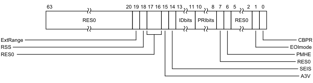
Image text
63 20 19 18 17 16 15 14 13 11 10 8 7 6 5 2 1 0
RES0 IDbits PRIbits RES0
ExtRange CBPR
RSS EOImode
RES0 PMHE
RES0
SEIS
A3V
ExtRange, bit [19]
Extended INTID range (read-only).
0b0 CPU interface does not support INTIDs in the range 1024..8191.
- Behaviour is UNPREDICTABLE if the IRI delivers an interrupt in the range 1024 to 8191 to the CPU interface.
Note Arm strongly recommends that the IRI is not configured to deliver interrupts in this range to a PE that does not support them.
0b1 CPU interface supports INTIDs in the range 1024..8191
- All INTIDs in the range 1024..8191 are treated as requiring deactivation.
If EL3 is implemented, ICC_CTLR_EL1.ExtRange is an alias of ICC_CTLR_EL3.ExtRange.
RSS, bit [18]
Range Selector Support. Possible values are:
0b0 Targeted SGIs with affinity level 0 values of 0 - 15 are supported. 0b1 Targeted SGIs with affinity level 0 values of 0 - 255 are supported. This bit is read-only.
Bits [17:16]
Reserved, RES0.
A3V, bit [15]
Affinity 3 Valid. Read-only and writes are ignored. Possible values are:
0b0 The CPU interface logic only supports zero values of Affinity 3 in SGI generation System registers. 0b1 The CPU interface logic supports non-zero values of Affinity 3 in SGI generation System registers.
If EL3 is implemented, this bit is an alias of ICC_CTLR_EL3.A3V.
SEIS, bit [14]
SEI Support. Read-only and writes are ignored. Indicates whether the CPU interface supports local generation of SEIs:
0b0 The CPU interface logic does not support local generation of SEIs. 0b1 The CPU interface logic supports local generation of SEIs.
If EL3 is implemented, this bit is an alias of ICC_CTLR_EL3.SEIS.
IDbits, bits [13:11]
Identifier bits. Read-only and writes are ignored. The number of physical interrupt identifier bits supported:
0b000 16 bits. 0b001 24 bits. All other values are reserved.
If EL3 is implemented, this field is an alias of ICC_CTLR_EL3.IDbits.
PRIbits, bits [10:8]
Priority bits. Read-only and writes are ignored. The number of priority bits implemented, minus one.
An implementation that supports two Security states must implement at least 32 levels of physical priority (5 priority bits).
An implementation that supports only a single Security state must implement at least 16 levels of physical priority (4 priority bits).
Note
This field always returns the number of priority bits implemented, regardless of the Security state of the access or the value of GICD_CTLR.DS.
For physical accesses, this field determines the minimum value of ICC_BPR0_EL1.
If EL3 is implemented, physical accesses return the value from ICC_CTLR_EL3.PRIbits.
If EL3 is not implemented, physical accesses return the value from this field.
Bit [7]
Reserved, RES0.
PMHE, bit [6]
Priority Mask Hint Enable. Controls whether the priority mask register is used as a hint for interrupt distribution:
0b0 Disables use of ICC_PMR_EL1 as a hint for interrupt distribution. 0b1 Enables use of ICC_PMR_EL1 as a hint for interrupt distribution. If EL3 is implemented, this bit is an alias of ICC_CTLR_EL3.PMHE. Whether this bit can be written as part of an access to this register depends on the value of GICD_CTLR.DS:
-
If GICD_CTLR.DS == 0, this bit is read-only.
-
If GICD_CTLR.DS == 1, this bit is read/write.
-
If EL3 is not implemented, it is IMPLEMENTATION DEFINED whether this bit is read-only or read-write:
-
If this bit is read-only, an implementation can choose to make this field RAZ/WI or RAO/WI.
-
If this bit is read/write, it resets to zero.
Bits [5:2]
Reserved, RES0.
EOImode, bit [1]
EOI mode for the current Security state. Controls whether a write to an End of Interrupt register also deactivates the interrupt:
0b0 ICC_EOIR0_EL1 and ICC_EOIR1_EL1 provide both priority drop and interrupt deactivation functionality. Accesses to ICC_DIR_EL1 are UNPREDICTABLE. 0b1 ICC_EOIR0_EL1 and ICC_EOIR1_EL1 provide priority drop functionality only. ICC_DIR_EL1 provides interrupt deactivation functionality.
The Secure ICC_CTLR_EL1.EOImode is an alias of ICC_CTLR_EL3.EOImode_EL1S.
The Non-secure ICC_CTLR_EL1.EOImode is an alias of ICC_CTLR_EL3.EOImode_EL1NS
CBPR, bit [0]
Common Binary Point Register. Controls whether the same register is used for interrupt preemption of both Group 0 and Group 1 interrupts:
0b0 ICC_BPR0_EL1 determines the preemption group for Group 0 interrupts only. ICC_BPR1_EL1 determines the preemption group for Group 1 interrupts.
0b1 ICC_BPR0_EL1 determines the preemption group for both Group 0 and Group 1 interrupts.
If EL3 is implemented:
-
This bit is an alias of ICC_CTLR_EL3.CBPR_EL1{S,NS} where S or NS corresponds to the current Security state.
-
If GICD_CTLR.DS == 0, this bit is read-only.
-
If GICD_CTLR.DS == 1, this bit is read/write.
If EL3 is not implemented, this bit is read/write.
On a Warm reset, this field resets to an architecturally UNKNOWN value.
Accessing the ICC_CTLR_EL1
Accesses to this register use the following encodings in the System instruction encoding space:
MRS , ICC_CTLR_EL1
| op0 | op1 | CRn | CRm | op2 |
|---|---|---|---|---|
| 0b11 | 0b000 | 0b1100 | 0b1100 | 0b100 |
if PSTATE.EL == EL0 then UNDEFINED;
elsif PSTATE.EL == EL1 then
    if Halted() && HaveEL(EL3) && EDSCR.SDD == '1' &&
    boolean IMPLEMENTATION_DEFINED "EL3 trap priority
when SDD == '1'" && SCR_EL3.<IRQ,FIQ> == '11' then
UNDEFINED;
elsif ICC_SRE_EL1.SRE == '0'
    then AArch64.SystemAccessTrap(EL1, 0x18);
elsif EL2Enabled() && ICH_HCR_EL2.TC == '1'
    then AArch64.SystemAccessTrap(EL2, 0x18);
elsif EL2Enabled() && HCR_EL2.FMO == '1'
    then return ICV_CTLR_EL1;
elsif EL2Enabled() && HCR_EL2.IMO == '1'
    then return ICV_CTLR_EL1;
elsif HaveEL(EL3) && SCR_EL3.<IRQ,FIQ> == '11'
    then if Halted() && EDSCR.SDD == '1'
    then UNDEFINED;
else AArch64.SystemAccessTrap(EL3, 0x18);
elsif HaveEL(EL3)
    then if SCR_EL3.NS == '0'
    then return ICC_CTLR_EL1_S;
else return ICC_CTLR_EL1_NS;
else return ICC_CTLR_EL1;
elsif PSTATE.EL == EL2
    then if Halted() && HaveEL(EL3) && EDSCR.SDD == '1' && boolean IMPLEMENTATION_DEFINED "EL3 trap priority when SDD == '1'" && SCR_EL3.<IRQ,FIQ> == '11'
    then UNDEFINED;
elsif ICC_SRE_EL2.SRE == '0'
    then AArch64.SystemAccessTrap(EL2, 0x18);
elsif HaveEL(EL3) && SCR_EL3.<IRQ,FIQ> == '11'
    then if Halted() && EDSCR.SDD == '1'
    then UNDEFINED;
else AArch64.SystemAccessTrap(EL3, 0x18);
elsif HaveEL(EL3)
    then if SCR_EL3.NS == '0'
    then return ICC_CTLR_EL1_S;
else return ICC_CTLR_EL1_NS;
else return ICC_CTLR_EL1;
elsif PSTATE.EL == EL3
    then if ICC_SRE_EL3.SRE == '0'
    then AArch64.SystemAccessTrap(EL3, 0x18);
else if SCR_EL3.NS == '0'
    then return ICC_CTLR_EL1_S;
else return ICC_CTLR_EL1_NS;
MSR ICC_CTLR_EL1,
| op0 | op1 | CRn | CRm | op2 |
|---|---|---|---|---|
| 0b11 | 0b000 | 0b1100 | 0b1100 | 0b100 |
if PSTATE.EL == EL0 then UNDEFINED;
elsif PSTATE.EL == EL1 then
    if Halted() && HaveEL(EL3) && EDSCR.SDD == '1' &&
    boolean IMPLEMENTATION_DEFINED "EL3 trap priority
when SDD == '1'" && SCR_EL3.<IRQ,FIQ> == '11' then
UNDEFINED;
elsif ICC_SRE_EL1.SRE == '0'
    then AArch64.SystemAccessTrap(EL1, 0x18);
elsif EL2Enabled() && ICH_HCR_EL2.TC == '1'
    then AArch64.SystemAccessTrap(EL2, 0x18);
elsif EL2Enabled() && HCR_EL2.FMO == '1' then
ICV_CTLR_EL1 = X[t];
elsif EL2Enabled() && HCR_EL2.IMO == '1'
    then ICV_CTLR_EL1 = X[t];
elsif HaveEL(EL3) && SCR_EL3.<IRQ,FIQ> == '11'
    then if Halted() && EDSCR.SDD == '1'
    then UNDEFINED;
else AArch64.SystemAccessTrap(EL3, 0x18);
elsif HaveEL(EL3)
    then if SCR_EL3.NS == '0'
    then ICC_CTLR_EL1_S = X[t];
else ICC_CTLR_EL1_NS = X[t];
else ICC_CTLR_EL1 = X[t];
elsif PSTATE.EL == EL2
    then if Halted() && HaveEL(EL3) && EDSCR.SDD == '1' && boolean IMPLEMENTATION_DEFINED "EL3 trap priority when SDD == '1'" && SCR_EL3.<IRQ,FIQ> == '11'
    then UNDEFINED;
elsif ICC_SRE_EL2.SRE == '0'
    then AArch64.SystemAccessTrap(EL2, 0x18);
elsif HaveEL(EL3) && SCR_EL3.<IRQ,FIQ> == '11'
    then if Halted() && EDSCR.SDD == '1'
    then UNDEFINED;
else AArch64.SystemAccessTrap(EL3, 0x18);
elsif HaveEL(EL3)
    then if SCR_EL3.NS == '0'
    then ICC_CTLR_EL1_S = X[t];
else ICC_CTLR_EL1_NS = X[t];
else ICC_CTLR_EL1 = X[t];
elsif PSTATE.EL == EL3
    then if ICC_SRE_EL3.SRE == '0'
    then AArch64.SystemAccessTrap(EL3, 0x18);
else if SCR_EL3.NS == '0'
    then ICC_CTLR_EL1_S = X[t];
else ICC_CTLR_EL1_NS = X[t];
12.2.7 ICC_CTLR_EL3, Interrupt Controller Control Register (EL3)
The ICC_CTLR_EL3 characteristics are:
Purpose
Controls aspects of the behavior of the GIC CPU interface and provides information about the features implemented.
Configurations
AArch64 System register ICC_CTLR_EL3 bits [31:0] can be mapped to AArch32 System register ICC_MCTLR[31:0], but this is not architecturally mandated.
This register is present only when EL3 is implemented. Otherwise, direct accesses to ICC_CTLR_EL3 are UNDEFINED.
Attributes
ICC_CTLR_EL3 is a 64-bit register.
Field descriptions
The ICC_CTLR_EL3 bit assignments are:
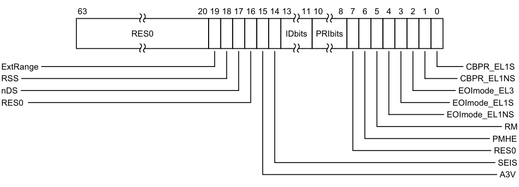
Image text
63 20 19 18 17 16 15 14 13 11 10 8 7 6 5 4 3 2 1 0
RES0 IDbits PRIbits
ExtRange CBPR_EL1S
RSS CBPR_EL1NS
nDS EOImode_EL3
RES0 EOImode_EL1S
EOImode_EL1NS
RM
PMHE
RES0
SEIS
A3V
ExtRange, bit [19]
Extended INTID range (read-only).
-
0b0 CPU interface does not support INTIDs in the range 1024..8191.
- Behaviour is UNPREDICTABLE if the IRI delivers an interrupt in the range 1024 to 8191 to the CPU interface.
Note Arm strongly recommends that the IRI is not configured to deliver interrupts in this range to a PE that does not support them.
-
0b1 CPU interface supports INTIDs in the range 1024..8191
- All INTIDs in the range 1024..8191 are treated as requiring deactivation.
RSS, bit [18]
Range Selector Support. 0b0 Targeted SGIs with affinity level 0 values of 0-15 are supported. 0b1 Targeted SGIs with affinity level 0 values of 0-255 are supported. This bit is read-only.
nDS, bit [17]
Disable Security not supported. Read-only and writes are ignored.
0b0 The CPU interface logic supports disabling of security. 0b1 The CPU interface logic does not support disabling of security, and requires that security is not disabled.
Bit [16]
Reserved, RES0.
A3V, bit [15]
Affinity 3 Valid. Read-only and writes are ignored.
0b0 The CPU interface logic does not support non-zero values of the Aff3 field in SGI generation System registers. 0b1 The CPU interface logic supports non-zero values of the Aff3 field in SGI generation System registers.
If EL3 is present, ICC_CTLR_EL1.A3V is an alias of ICC_CTLR_EL3.A3V
SEIS, bit [14]
SEI Support. Read-only and writes are ignored. Indicates whether the CPU interface supports generation of SEIs: 0b0 The CPU interface logic does not support generation of SEIs. 0b1 The CPU interface logic supports generation of SEIs.
If EL3 is present, ICC_CTLR_EL1.SEIS is an alias of ICC_CTLR_EL3.SEIS
IDbits, bits [13:11]
Identifier bits. Read-only and writes are ignored. Indicates the number of physical interrupt identifier bits supported.
0b000 16 bits. 0b001 24 bits. All other values are reserved.
If EL3 is present, ICC_CTLR_EL1.IDbits is an alias of ICC_CTLR_EL3.IDbits
PRIbits, bits [10:8]
Priority bits. Read-only and writes are ignored. The number of priority bits implemented, minus one.
An implementation that supports two Security states must implement at least 32 levels of physical priority (5 priority bits).
An implementation that supports only a single Security state must implement at least 16 levels of physical priority (4 priority bits).
Note This field always returns the number of priority bits implemented, regardless of the value of SCR_EL3.NS or the value of GICD_CTLR.DS.
The division between group priority and subpriority is defined in the binary point registers ICC_BPR0_EL1 and ICC_BPR1_EL1. This field determines the minimum value of ICC_BPR0_EL1.
Bit [7]
Reserved, RES0.
PMHE, bit [6]
Priority Mask Hint Enable.
0b0 Disables use of the priority mask register as a hint for interrupt distribution. 0b1 Enables use of the priority mask register as a hint for interrupt distribution.
Software must write ICC_PMR_EL1 to 0xFF before clearing this field to 0.
-
An implementation might choose to make this field RAO/WI if priority-based routing is always used
-
An implementation might choose to make this field RAZ/WI if priority-based routing is never used
If EL3 is present, ICC_CTLR_EL1.PMHE is an alias of ICC_CTLR_EL3.PMHE. On a Warm reset, this field resets to 0.
RM, bit [5]
Routing Modifier. For legacy operation of EL1 software with GICC_CTLR.FIQEn set to 1, this bit indicates whether interrupts can be acknowledged or observed as the Highest Priority Pending Interrupt, or whether a special INTID value is returned.
Possible values of this bit are:
0b0 Secure Group 0 and Non-secure Group 1 interrupts can be acknowledged and observed as the highest priority interrupt at the Secure Exception level where the interrupt is taken.
0b1 When accessed at EL3 in AArch64 state:
• Secure Group 0 interrupts return a special INTID value of 1020. This affects accesses to ICC_IAR0_EL1 and ICC_HPPIR0_EL1.
• Non-secure Group 1 interrupts return a special INTID value of 1021. This affects accesses to ICC_IAR1_EL1 and ICC_HPPIR1_EL1.
Note The Routing Modifier bit is supported in AArch64 only. In systems without EL3 the behavior is as if the value is 0. Software must ensure this bit is 0 when the Secure copy of ICC_SRE_EL1.SRE is 1, otherwise system behavior is UNPREDICTABLE. In systems without EL3 or where the Secure copy of ICC_SRE_EL1.SRE is RAO/WI, this bit is RES0.
On a Warm reset, this field resets to an architecturally UNKNOWN value.
EOImode_EL1NS, bit [4]
EOI mode for interrupts handled at Non-secure EL1 and EL2. Controls whether a write to an End of Interrupt register also deactivates the interrupt.
0b0 ICC_EOIR0_EL1 and ICC_EOIR1_EL1 provide both priority drop and interrupt deactivation functionality. Accesses to ICC_DIR_EL1 are UNPREDICTABLE.
0b1 ICC_EOIR0_EL1 and ICC_EOIR1_EL1 provide priority drop functionality only. ICC_DIR_EL1 provides interrupt deactivation functionality.
If EL3 is present, ICC_CTLR_EL1(NS).EOImode is an alias of ICC_CTLR_EL3.EOImode_EL1NS.
On a Warm reset, this field resets to an architecturally UNKNOWN value.
EOImode_EL1S, bit [3]
EOI mode for interrupts handled at Secure EL1 and EL2. Controls whether a write to an End of Interrupt register also deactivates the interrupt.
0b0 ICC_EOIR0_EL1 and ICC_EOIR1_EL1 provide both priority drop and interrupt deactivation functionality. Accesses to ICC_DIR_EL1 are UNPREDICTABLE.
0b1 ICC_EOIR0_EL1 and ICC_EOIR1_EL1 provide priority drop functionality only. ICC_DIR_EL1 provides interrupt deactivation functionality.
If EL3 is present, ICC_CTLR_EL1(S).EOImode is an alias of ICC_CTLR_EL3.EOImode_EL1S.
On a Warm reset, this field resets to an architecturally UNKNOWN value.
EOImode_EL3, bit [2]
EOI mode for interrupts handled at EL3. Controls whether a write to an End of Interrupt register also deactivates the interrupt.
0b0 ICC_EOIR0_EL1 and ICC_EOIR1_EL1 provide both priority drop and interrupt deactivation functionality. Accesses to ICC_DIR_EL1 are UNPREDICTABLE.
0b1 ICC_EOIR0_EL1 and ICC_EOIR1_EL1 provide priority drop functionality only. ICC_DIR_EL1 provides interrupt deactivation functionality.
On a Warm reset, this field resets to an architecturally UNKNOWN value.
CBPR_EL1NS, bit [1]
Common Binary Point Register, EL1 Non-secure. Controls whether the same register is used for interrupt preemption of both Group 0 and Group 1 Non-secure interrupts at EL1 and EL2.
0b0 ICC_BPR0_EL1 determines the preemption group for Group 0 interrupts only. ICC_BPR1_EL1 determines the preemption group for Non-secure Group 1 interrupts.
0b1 ICC_BPR0_EL1 determines the preemption group for Group 0 interrupts and Non-secure Group 1 interrupts. Non-secure accesses to GICC_BPR and ICC_BPR1_EL1 access the state of ICC_BPR0_EL1.
If EL3 is present, ICC_CTLR_EL1(NS).CBPR is an alias of ICC_CTLR_EL3.CBPR_EL1NS.
On a Warm reset, this field resets to an architecturally UNKNOWN value.
CBPR_EL1S, bit [0]
Common Binary Point Register, EL1 Secure. Controls whether the same register is used for interrupt preemption of both Group 0 and Group 1 Secure interrupts at EL1 and EL2.
0b0 ICC_BPR0_EL1 determines the preemption group for Group 0 interrupts only. ICC_BPR1_EL1 determines the preemption group for Secure Group 1 interrupts.
0b1 ICC_BPR0_EL1 determines the preemption group for Group 0 interrupts and Secure Group 1 interrupts. Secure EL1 accesses to ICC_BPR1_EL1 access the state of ICC_BPR0_EL1.
If EL3 is present, ICC_CTLR_EL1(S).CBPR is an alias of ICC_CTLR_EL3.CBPR_EL1S.
On a Warm reset, this field resets to an architecturally UNKNOWN value.
Accessing the ICC_CTLR_EL3
Accesses to this register use the following encodings in the System instruction encoding space:
MRS , ICC_CTLR_EL3
| op0 | op1 | CRn | CRm | op2 |
|---|---|---|---|---|
| 0b11 | 0b110 | 0b1100 | 0b1100 | 0b100 |
if PSTATE.EL == EL0 then UNDEFINED;
elsif PSTATE.EL == EL1 then UNDEFINED;
elsif PSTATE.EL == EL2 then UNDEFINED;
elsif PSTATE.EL == EL3 then
    if ICC_SRE_EL3.SRE == '0' then AArch64.SystemAccessTrap(EL3, 0x18);
else return ICC_CTLR_EL3;
MSR ICC_CTLR_EL3,
| op0 | op1 | CRn | CRm | op2 |
|---|---|---|---|---|
| 0b11 | 0b110 | 0b1100 | 0b1100 | 0b100 |
if PSTATE.EL == EL0 then UNDEFINED;
elsif PSTATE.EL == EL1 then UNDEFINED;
elsif PSTATE.EL == EL2 then UNDEFINED;
elsif PSTATE.EL == EL3 then
    if ICC_SRE_EL3.SRE == '0' then AArch64.SystemAccessTrap(EL3, 0x18);
else ICC_CTLR_EL3 = X[t];
12.2.8 ICC_DIR_EL1, Interrupt Controller Deactivate Interrupt Register
The ICC_DIR_EL1 characteristics are:
Purpose
When interrupt priority drop is separated from interrupt deactivation, a write to this register deactivates the specified interrupt.
Configurations
AArch64 System register ICC_DIR_EL1 performs the same function as AArch32 System register ICC_DIR.
Attributes
ICC_DIR_EL1 is a 64-bit register.
Field descriptions
The ICC_DIR_EL1 bit assignments are:

63 24 23 0
RES0 INTID
Bits [63:24]
Reserved, RES0.
INTID, bits [23:0]
The INTID of the interrupt to be deactivated.
This field has either 16 or 24 bits implemented. The number of implemented bits can be found in ICC_CTLR_EL1.IDbits and ICC_CTLR_EL3.IDbits. If only 16 bits are implemented, bits [23:16] of this register are RES0.
Accessing the ICC_DIR_EL1
There are two cases when writing to ICC_DIR_EL1 that were UNPREDICTABLE for a corresponding GICv2 write to GICC_DIR:
-
When EOImode == 0. GICv3 implementations must ignore such writes. In systems supporting system error generation, an implementation might generate an SEI.
-
When EOImode == 1 but no EOI has been issued. The interrupt will be de-activated by the Distributor, however the active priority in the CPU interface for the interrupt will remain set (because no EOI was issued).
Accesses to this register use the following encodings in the System instruction encoding space:
MSR ICC_DIR_EL1,
| op0 | op1 | CRn | CRm | op2 |
|---|---|---|---|---|
| 0b11 | 0b000 | 0b1100 | 0b1011 | 0b001 |
if PSTATE.EL == EL0 then UNDEFINED;
elsif PSTATE.EL == EL1 then
    if Halted() && HaveEL(EL3) && EDSCR.SDD == '1' &&
    boolean IMPLEMENTATION_DEFINED "EL3 trap priority
when SDD == '1'" && SCR_EL3.<IRQ,FIQ> == '11' then
UNDEFINED;
elsif ICC_SRE_EL1.SRE == '0' then AArch64.SystemAccessTrap(EL1, 0x18);
elsif EL2Enabled() && ICH_HCR_EL2.TDIR == '1' then AArch64.SystemAccessTrap(EL2, 0x18);
elsif EL2Enabled() && ICH_HCR_EL2.TC == '1' then AArch64.SystemAccessTrap(EL2, 0x18);
elsif EL2Enabled() && HCR_EL2.FMO == '1' then ICV_DIR_EL1 = X[t];
elsif EL2Enabled() && HCR_EL2.IMO == '1' then ICV_DIR_EL1 = X[t];
elsif HaveEL(EL3) && SCR_EL3.<IRQ,FIQ> == '11' then
    if Halted() && EDSCR.SDD == '1' then UNDEFINED;
else AArch64.SystemAccessTrap(EL3, 0x18);
else ICC_DIR_EL1 = X[t];
elsif PSTATE.EL == EL2 then
    if Halted() && HaveEL(EL3) && EDSCR.SDD == '1' &&
    boolean IMPLEMENTATION_DEFINED "EL3 trap priority
when SDD == '1'" && SCR_EL3.<IRQ,FIQ> == '11' then UNDEFINED;
elsif ICC_SRE_EL2.SRE == '0' then AArch64.SystemAccessTrap(EL2, 0x18);
elsif HaveEL(EL3) && SCR_EL3.<IRQ,FIQ> == '11' then
    if Halted() && EDSCR.SDD == '1' then UNDEFINED;
else AArch64.SystemAccessTrap(EL3, 0x18);
else ICC_DIR_EL1 = X[t];
elsif PSTATE.EL == EL3 then
    if ICC_SRE_EL3.SRE == '0' then AArch64.SystemAccessTrap(EL3, 0x18);
else ICC_DIR_EL1 = X[t];
12.2.9 ICC_EOIR0_EL1, Interrupt Controller End Of Interrupt Register 0
The ICC_EOIR0_EL1 characteristics are:
Purpose
A PE writes to this register to inform the CPU interface that it has completed the processing of the specified Group 0 interrupt.
Configurations
AArch64 System register ICC_EOIR0_EL1 performs the same function as AArch32 System register ICC_EOIR0.
Attributes
ICC_EOIR0_EL1 is a 64-bit register.
Field descriptions
The ICC_EOIR0_EL1 bit assignments are:

63 24 23 0
RES0 INTID
Bits [63:24]
Reserved, RES0.
INTID, bits [23:0]
The INTID from the corresponding ICC_IAR0_EL1 access.
This field has either 16 or 24 bits implemented. The number of implemented bits can be found in ICC_CTLR_EL1.IDbits and ICC_CTLR_EL3.IDbits. If only 16 bits are implemented, bits [23:16] of this register are RES0.
If the EOImode bit for the current Exception level and Security state is 0, a write to this register drops the priority for the interrupt, and also deactivates the interrupt.
If the EOImode bit for the current Exception level and Security state is 1, a write to this register only drops the priority for the interrupt. Software must write to ICC_DIR_EL1 to deactivate the interrupt.
The EOImode bit for the current Exception level and Security state is determined as follows:
-
If EL3 is not implemented, the appropriate bit is ICC_CTLR_EL1.EOIMode.
-
If EL3 is implemented and the software is executing at EL3, the appropriate bit is ICC_CTLR_EL3.EOImode_EL3.
-
If EL3 is implemented and the software is not executing at EL3, the bit depends on the current Security state:
- If the software is executing in Secure state, the bit is ICC_CTLR_EL3.EOImode_EL1S.
-
If the software is executing in Non-secure state, the bit is ICC_CTLR_EL3.EOImode_EL1NS.
Accessing the ICC_EOIR0_EL1
A write to this register must correspond to the most recent valid read by this PE from an Interrupt Acknowledge Register, and must correspond to the INTID that was read from ICC_IAR0_EL1, otherwise the system behavior is UNPREDICTABLE. A valid read is a read that returns a valid INTID that is not a special INTID.
A write of a Special INTID is ignored. For more information, see Special INTIDs. Accesses to this register use the following encodings in the System instruction encoding space:
MSR ICC_EOIR0_EL1,
| op0 | op1 | CRn | CRm | op2 |
|---|---|---|---|---|
| 0b11 | 0b000 | 0b1100 | 0b1000 | 0b001 |
if PSTATE.EL == EL0 then UNDEFINED;
elsif PSTATE.EL == EL1 then
    if Halted() && HaveEL(EL3) && EDSCR.SDD == '1' &&
    boolean IMPLEMENTATION_DEFINED "EL3 trap priority
when SDD == '1'" && SCR_EL3.FIQ == '1' then UNDEFINED;
elsif ICC_SRE_EL1.SRE == '0' then AArch64.SystemAccessTrap(EL1, 0x18);
elsif EL2Enabled() && ICH_HCR_EL2.TALL0 == '1' then AArch64.SystemAccessTrap(EL2, 0x18);
elsif EL2Enabled() && HCR_EL2.FMO == '1' then ICV_EOIR0_EL1 = X[t];
elsif HaveEL(EL3) && SCR_EL3.FIQ == '1' then
    if Halted() && EDSCR.SDD == '1' then UNDEFINED;
else AArch64.SystemAccessTrap(EL3, 0x18);
else ICC_EOIR0_EL1 = X[t];
elsif PSTATE.EL == EL2 then
    if Halted() && HaveEL(EL3) && EDSCR.SDD == '1' &&
    boolean IMPLEMENTATION_DEFINED "EL3 trap priority
when SDD == '1'" && SCR_EL3.FIQ == '1' then UNDEFINED;
elsif ICC_SRE_EL2.SRE == '0' then AArch64.SystemAccessTrap(EL2, 0x18);
elsif HaveEL(EL3) && SCR_EL3.FIQ == '1' then
    if Halted() && EDSCR.SDD == '1' then UNDEFINED;
else AArch64.SystemAccessTrap(EL3, 0x18);
else ICC_EOIR0_EL1 = X[t];
elsif PSTATE.EL == EL3 then
    if ICC_SRE_EL3.SRE == '0' then AArch64.SystemAccessTrap(EL3, 0x18);
else ICC_EOIR0_EL1 = X[t];
12.2.10 ICC_EOIR1_EL1, Interrupt Controller End Of Interrupt Register 1
The ICC_EOIR1_EL1 characteristics are:
Purpose
A PE writes to this register to inform the CPU interface that it has completed the processing of the specified Group 1 interrupt.
Configurations
AArch64 System register ICC_EOIR1_EL1 performs the same function as AArch32 System register ICC_EOIR1.
Attributes
ICC_EOIR1_EL1 is a 64-bit register.
Field descriptions
The ICC_EOIR1_EL1 bit assignments are:

63 24 23 0
RES0 INTID
Bits [63:24]
Reserved, RES0.
INTID, bits [23:0]
The INTID from the corresponding ICC_IAR1_EL1 access.
This field has either 16 or 24 bits implemented. The number of implemented bits can be found in ICC_CTLR_EL1.IDbits and ICC_CTLR_EL3.IDbits. If only 16 bits are implemented, bits [23:16] of this register are RES0.
If the EOImode bit for the current Exception level and Security state is 0, a write to this register drops the priority for the interrupt, and also deactivates the interrupt.
If the EOImode bit for the current Exception level and Security state is 1, a write to this register only drops the priority for the interrupt. Software must write to ICC_DIR_EL1 to deactivate the interrupt.
The EOImode bit for the current Exception level and Security state is determined as follows:
-
If EL3 is not implemented, the appropriate bit is ICC_CTLR_EL1.EOIMode.
-
If EL3 is implemented and the software is executing at EL3, the appropriate bit is ICC_CTLR_EL3.EOImode_EL3.
-
If EL3 is implemented and the software is not executing at EL3, the bit depends on the current Security state:
- If the software is executing in Secure state, the bit is ICC_CTLR_EL3.EOImode_EL1S.
-
If the software is executing in Non-secure state, the bit is ICC_CTLR_EL3.EOImode_EL1NS.
Accessing the ICC_EOIR1_EL1
A write to this register must correspond to the most recent valid read by this PE from an Interrupt Acknowledge Register, and must correspond to the INTID that was read from ICC_IAR1_EL1, otherwise the system behavior is UNPREDICTABLE. A valid read is a read that returns a valid INTID that is not a special INTID.
A write of a Special INTID is ignored. For more information, see Special INTIDs. Accesses to this register use the following encodings in the System instruction encoding space:
MSR ICC_EOIR1_EL1,
| op0 | op1 | CRn | CRm | op2 |
|---|---|---|---|---|
| 0b11 | 0b000 | 0b1100 | 0b1100 | 0b001 |
if PSTATE.EL == EL0 then UNDEFINED;
elsif PSTATE.EL == EL1 then
    if Halted() && HaveEL(EL3) && EDSCR.SDD == '1' &&
    boolean IMPLEMENTATION_DEFINED "EL3 trap priority
when SDD == '1'" && SCR_EL3.IRQ == '1' then UNDEFINED;
elsif ICC_SRE_EL1.SRE == '0' then AArch64.SystemAccessTrap(EL1, 0x18);
elsif EL2Enabled() && ICH_HCR_EL2.TALL1 == '1' then AArch64.SystemAccessTrap(EL2, 0x18);
elsif EL2Enabled() && HCR_EL2.IMO == '1' then ICV_EOIR1_EL1 = X[t];
elsif HaveEL(EL3) && SCR_EL3.IRQ == '1' then
    if Halted() && EDSCR.SDD == '1' then UNDEFINED;
else AArch64.SystemAccessTrap(EL3, 0x18);
else ICC_EOIR1_EL1 = X[t];
elsif PSTATE.EL == EL2 then
    if Halted() && HaveEL(EL3) && EDSCR.SDD == '1' &&
    boolean IMPLEMENTATION_DEFINED "EL3 trap priority
when SDD == '1'" && SCR_EL3.IRQ == '1' then UNDEFINED;
elsif ICC_SRE_EL2.SRE == '0' then AArch64.SystemAccessTrap(EL2, 0x18);
elsif HaveEL(EL3) && SCR_EL3.IRQ == '1' then
    if Halted() && EDSCR.SDD == '1' then UNDEFINED;
else AArch64.SystemAccessTrap(EL3, 0x18);
else ICC_EOIR1_EL1 = X[t];
elsif PSTATE.EL == EL3 then
    if ICC_SRE_EL3.SRE == '0' then AArch64.SystemAccessTrap(EL3, 0x18);
else ICC_EOIR1_EL1 = X[t];
12.2.11 ICC_HPPIR0_EL1, Interrupt Controller Highest Priority Pending Interrupt Register 0
The ICC_HPPIR0_EL1 characteristics are:
Purpose
Indicates the highest priority pending Group 0 interrupt on the CPU interface.
Configurations
AArch64 System register ICC_HPPIR0_EL1 performs the same function as AArch32 System register ICC_HPPIR0.
Attributes
ICC_HPPIR0_EL1 is a 64-bit register.
Field descriptions
The ICC_HPPIR0_EL1 bit assignments are:
| | 63 | | 24 | 23 | | 0 | | |—|—|—|—|—|—|—| |||||||||
Bits [63:24]
Reserved, RES0.
INTID, bits [23:0]
The INTID of the highest priority pending interrupt, if that interrupt is observable at the current Security state and Exception level.
If the highest priority pending interrupt is not observable, this field contains a special INTID to indicate the reason. These special INTIDs can be one of: 1020, 1021, or 1023. For more information, see Special INTIDs.
This field has either 16 or 24 bits implemented. The number of implemented bits can be found in ICC_CTLR_EL1.IDbits and ICC_CTLR_EL3.IDbits. If only 16 bits are implemented, bits [23:16] of this register are RES0.
Accessing the ICC_HPPIR0_EL1
Accesses to this register use the following encodings in the System instruction encoding space:
MRS , ICC_HPPIR0_EL1
| op0 | op1 | CRn | CRm | op2 |
|---|---|---|---|---|
| 0b11 | 0b000 | 0b1100 | 0b1000 | 0b010 |
if PSTATE.EL == EL0 then UNDEFINED;
elsif PSTATE.EL == EL1 then
    if Halted() && HaveEL(EL3) && EDSCR.SDD == '1' &&
    boolean IMPLEMENTATION_DEFINED "EL3 trap priority
when SDD == '1'" && SCR_EL3.FIQ == '1' then
UNDEFINED;
elsif ICC_SRE_EL1.SRE == '0' then AArch64.SystemAccessTrap(EL1, 0x18);
elsif EL2Enabled() && ICH_HCR_EL2.TALL0 == '1' then AArch64.SystemAccessTrap(EL2, 0x18);
elsif EL2Enabled() && HCR_EL2.FMO == '1' then
    return ICV_HPPIR0_EL1;
elsif HaveEL(EL3) && SCR_EL3.FIQ == '1' then
    if Halted() && EDSCR.SDD == '1' then UNDEFINED;
else AArch64.SystemAccessTrap(EL3, 0x18);
else return ICC_HPPIR0_EL1;
elsif PSTATE.EL == EL2 then
    if Halted() && HaveEL(EL3) && EDSCR.SDD == '1' &&
    boolean IMPLEMENTATION_DEFINED "EL3 trap priority
when SDD == '1'" && SCR_EL3.FIQ == '1' then UNDEFINED;
elsif ICC_SRE_EL2.SRE == '0' then AArch64.SystemAccessTrap(EL2, 0x18);
elsif HaveEL(EL3) && SCR_EL3.FIQ == '1' then
    if Halted() && EDSCR.SDD == '1' then UNDEFINED;
else AArch64.SystemAccessTrap(EL3, 0x18);
else return ICC_HPPIR0_EL1;
elsif PSTATE.EL == EL3 then
    if ICC_SRE_EL3.SRE == '0' then AArch64.SystemAccessTrap(EL3, 0x18);
else return ICC_HPPIR0_EL1;
12.2.12 ICC_HPPIR1_EL1, Interrupt Controller Highest Priority Pending Interrupt Register 1
The ICC_HPPIR1_EL1 characteristics are:
Purpose
Indicates the highest priority pending Group 1 interrupt on the CPU interface.
Configurations
AArch64 System register ICC_HPPIR1_EL1 performs the same function as AArch32 System register ICC_HPPIR1.
Attributes
ICC_HPPIR1_EL1 is a 64-bit register.
Field descriptions
The ICC_HPPIR1_EL1 bit assignments are:
| | 63 | | 24 | 23 | | 0 | | |—|—|—|—|—|—|—| |||||||||
Bits [63:24]
Reserved, RES0.
INTID, bits [23:0]
The INTID of the highest priority pending interrupt, if that interrupt is observable at the current Security state and Exception level.
If the highest priority pending interrupt is not observable, this field contains a special INTID to indicate the reason. These special INTIDs can be one of: 1020, 1021, or 1023. For more information, see Special INTIDs.
This field has either 16 or 24 bits implemented. The number of implemented bits can be found in ICC_CTLR_EL1.IDbits and ICC_CTLR_EL3.IDbits. If only 16 bits are implemented, bits [23:16] of this register are RES0.
Accessing the ICC_HPPIR1_EL1
Accesses to this register use the following encodings in the System instruction encoding space:
MRS , ICC_HPPIR1_EL1
| op0 | op1 | CRn | CRm | op2 |
|---|---|---|---|---|
| 0b11 | 0b000 | 0b1100 | 0b1100 | 0b010 |
if PSTATE.EL == EL0 then
UNDEFINED;
elsif PSTATE.EL == EL1 then

if Halted() && HaveEL(EL3) && EDSCR.SDD == '1' && boolean IMPLEMENTATION_DEFINED "EL3 trap priority when SDD == '1'" && SCR_EL3.IRQ == '1' then
UNDEFINED;
elsif ICC_SRE_EL1.SRE == '0' then AArch64.SystemAccessTrap(EL1, 0x18);
elsif EL2Enabled() && ICH_HCR_EL2.TALL1 == '1' then AArch64.SystemAccessTrap(EL2, 0x18);
elsif EL2Enabled() && HCR_EL2.IMO == '1' then
    return ICV_HPPIR1_EL1;
elsif HaveEL(EL3) && SCR_EL3.IRQ == '1' then
    if Halted() && EDSCR.SDD == '1' then UNDEFINED;
else AArch64.SystemAccessTrap(EL3, 0x18);
else return ICC_HPPIR1_EL1;
elsif PSTATE.EL == EL2 then
    if Halted() && HaveEL(EL3) && EDSCR.SDD == '1' &&
    boolean IMPLEMENTATION_DEFINED "EL3 trap priority
when SDD == '1'" && SCR_EL3.IRQ == '1' then UNDEFINED;
elsif ICC_SRE_EL2.SRE == '0' then AArch64.SystemAccessTrap(EL2, 0x18);
elsif HaveEL(EL3) && SCR_EL3.IRQ == '1' then
    if Halted() && EDSCR.SDD == '1' then UNDEFINED;
else AArch64.SystemAccessTrap(EL3, 0x18);
else return ICC_HPPIR1_EL1;
elsif PSTATE.EL == EL3 then
    if ICC_SRE_EL3.SRE == '0' then AArch64.SystemAccessTrap(EL3, 0x18);
else return ICC_HPPIR1_EL1;
12.2.13 ICC_IAR0_EL1, Interrupt Controller Interrupt Acknowledge Register 0
The ICC_IAR0_EL1 characteristics are:
Purpose
The PE reads this register to obtain the INTID of the signaled Group 0 interrupt. This read acts as an acknowledge for the interrupt.
Configurations
AArch64 System register ICC_IAR0_EL1 performs the same function as AArch32 System register ICC_IAR0.
To allow software to ensure appropriate observability of actions initiated by GIC register accesses, the PE and CPU interface logic must ensure that reads of this register are self-synchronising when interrupts are masked by the PE (that is when PSTATE.{I,F} == {0,0}). This ensures that the effect of activating an interrupt on the signaling of interrupt exceptions is observed when a read of this register is architecturally executed so that no spurious interrupt exception occurs if interrupts are unmasked by an instruction immediately following the read. For more information, see Observability of the effects of accesses to the GIC registers.
Attributes
ICC_IAR0_EL1 is a 64-bit register.
Field descriptions
The ICC_IAR0_EL1 bit assignments are:
| | 63 | | 24 | 23 | | 0 | | |—|—|—|—|—|—|—| |||||||||
Bits [63:24]
Reserved, RES0.
INTID, bits [23:0]
The INTID of the signaled interrupt.
This is the INTID of the highest priority pending interrupt, if that interrupt is of sufficient priority for it to be signaled to the PE, and if it can be acknowledged at the current Security state and Exception level.
If the highest priority pending interrupt is not observable, this field contains a special INTID to indicate the reason. These special INTIDs can be one of: 1020, 1021, or 1023. For more information, see Special INTIDs.
This field has either 16 or 24 bits implemented. The number of implemented bits can be found in ICC_CTLR_EL1.IDbits and ICC_CTLR_EL3.IDbits. If only 16 bits are implemented, bits [23:16] of this register are RES0.
Accessing the ICC_IAR0_EL1
Accesses to this register use the following encodings in the System instruction encoding space:
MRS , ICC_IAR0_EL1
| op0 | op1 | CRn | CRm | op2 |
|---|---|---|---|---|
| 0b11 | 0b000 | 0b1100 | 0b1000 | 0b000 |
if PSTATE.EL == EL0 then UNDEFINED;
elsif PSTATE.EL == EL1 then
    if Halted() && HaveEL(EL3) && EDSCR.SDD == '1' &&
    boolean IMPLEMENTATION_DEFINED "EL3 trap priority
when SDD == '1'" && SCR_EL3.FIQ == '1' then UNDEFINED;
elsif ICC_SRE_EL1.SRE == '0' then AArch64.SystemAccessTrap(EL1, 0x18);
elsif EL2Enabled() && ICH_HCR_EL2.TALL0 == '1' then AArch64.SystemAccessTrap(EL2, 0x18);
elsif EL2Enabled() && HCR_EL2.FMO == '1' then
    return ICV_IAR0_EL1;
elsif HaveEL(EL3) && SCR_EL3.FIQ == '1' then
    if Halted() && EDSCR.SDD == '1' then UNDEFINED;
else AArch64.SystemAccessTrap(EL3, 0x18);
else return ICC_IAR0_EL1;
elsif PSTATE.EL == EL2 then
    if Halted() && HaveEL(EL3) && EDSCR.SDD == '1' &&
    boolean IMPLEMENTATION_DEFINED "EL3 trap priority
when SDD == '1'" && SCR_EL3.FIQ == '1' then UNDEFINED;
elsif ICC_SRE_EL2.SRE == '0' then AArch64.SystemAccessTrap(EL2, 0x18);
elsif HaveEL(EL3) && SCR_EL3.FIQ == '1' then
    if Halted() && EDSCR.SDD == '1' then UNDEFINED;
else AArch64.SystemAccessTrap(EL3, 0x18);
else return ICC_IAR0_EL1;
elsif PSTATE.EL == EL3 then
    if ICC_SRE_EL3.SRE == '0' then AArch64.SystemAccessTrap(EL3, 0x18);
else return ICC_IAR0_EL1;
12.2.14 ICC_IAR1_EL1, Interrupt Controller Interrupt Acknowledge Register 1
The ICC_IAR1_EL1 characteristics are:
Purpose
The PE reads this register to obtain the INTID of the signaled Group 1 interrupt. This read acts as an acknowledge for the interrupt.
Configurations
AArch64 System register ICC_IAR1_EL1 performs the same function as AArch32 System register ICC_IAR1.
To allow software to ensure appropriate observability of actions initiated by GIC register accesses, the PE and CPU interface logic must ensure that reads of this register are self-synchronising when interrupts are masked by the PE (that is when PSTATE.{I,F} == {0,0}). This ensures that the effect of activating an interrupt on the signaling of interrupt exceptions is observed when a read of this register is architecturally executed so that no spurious interrupt exception occurs if interrupts are unmasked by an instruction immediately following the read. For more information, see Observability of the effects of accesses to the GIC registers.
Attributes
ICC_IAR1_EL1 is a 64-bit register.
Field descriptions
The ICC_IAR1_EL1 bit assignments are:
| | 63 | | 24 | 23 | | 0 | | |—|—|—|—|—|—|—| |||||||||
Bits [63:24]
Reserved, RES0.
INTID, bits [23:0]
The INTID of the signaled interrupt.
This is the INTID of the highest priority pending interrupt, if that interrupt is of sufficient priority for it to be signaled to the PE, and if it can be acknowledged at the current Security state and Exception level.
If the highest priority pending interrupt is not observable, this field contains a special INTID to indicate the reason. These special INTIDs can be one of: 1020, 1021, or 1023. For more information, see Special INTIDs.
This field has either 16 or 24 bits implemented. The number of implemented bits can be found in ICC_CTLR_EL1.IDbits and ICC_CTLR_EL3.IDbits. If only 16 bits are implemented, bits [23:16] of this register are RES0.
Accessing the ICC_IAR1_EL1
Accesses to this register use the following encodings in the System instruction encoding space:
MRS , ICC_IAR1_EL1
| op0 | op1 | CRn | CRm | op2 |
|---|---|---|---|---|
| 0b11 | 0b000 | 0b1100 | 0b1100 | 0b000 |
if PSTATE.EL == EL0 then UNDEFINED;
elsif PSTATE.EL == EL1 then
    if Halted() && HaveEL(EL3) && EDSCR.SDD == '1' &&
    boolean IMPLEMENTATION_DEFINED "EL3 trap priority
when SDD == '1'" && SCR_EL3.IRQ == '1' then UNDEFINED;
elsif ICC_SRE_EL1.SRE == '0' then AArch64.SystemAccessTrap(EL1, 0x18);
elsif EL2Enabled() && ICH_HCR_EL2.TALL1 == '1' then AArch64.SystemAccessTrap(EL2, 0x18);
elsif EL2Enabled() && HCR_EL2.IMO == '1' then
    return ICV_IAR1_EL1;
elsif HaveEL(EL3) && SCR_EL3.IRQ == '1' then
    if Halted() && EDSCR.SDD == '1' then UNDEFINED;
else AArch64.SystemAccessTrap(EL3, 0x18);
else return ICC_IAR1_EL1;
elsif PSTATE.EL == EL2 then
    if Halted() && HaveEL(EL3) && EDSCR.SDD == '1' &&
    boolean IMPLEMENTATION_DEFINED "EL3 trap priority
when SDD == '1'" && SCR_EL3.IRQ == '1' then UNDEFINED;
elsif ICC_SRE_EL2.SRE == '0' then AArch64.SystemAccessTrap(EL2, 0x18);
elsif HaveEL(EL3) && SCR_EL3.IRQ == '1' then
    if Halted() && EDSCR.SDD == '1' then UNDEFINED;
else AArch64.SystemAccessTrap(EL3, 0x18);
else return ICC_IAR1_EL1;
elsif PSTATE.EL == EL3 then
    if ICC_SRE_EL3.SRE == '0' then AArch64.SystemAccessTrap(EL3, 0x18);
else return ICC_IAR1_EL1;
12.2.15 ICC_IGRPEN0_EL1, Interrupt Controller Interrupt Group 0 Enable register
The ICC_IGRPEN0_EL1 characteristics are:
Purpose
Controls whether Group 0 interrupts are enabled or not.
Configurations
AArch64 System register ICC_IGRPEN0_EL1 bits [31:0] are architecturally mapped to AArch32 System register ICC_IGRPEN0[31:0].
Attributes
ICC_IGRPEN0_EL1 is a 64-bit register.
Field descriptions
The ICC_IGRPEN0_EL1 bit assignments are:

63 1 0
RES0
Enable
Bits [63:1]
Reserved, RES0.
Enable, bit [0]
Enables Group 0 interrupts.
0b0 Group 0 interrupts are disabled. 0b1 Group 0 interrupts are enabled.
Virtual accesses to this register update ICH_VMCR_EL2.VENG0.
If the highest priority pending interrupt for that PE is a Group 0 interrupt using 1 of N model, then the interrupt will be targeted to another PE as a result of the Enable bit changing from 1 to 0. On a Warm reset, this field resets to 0.
Accessing the ICC_IGRPEN0_EL1
Accesses to this register use the following encodings in the System instruction encoding space:
MRS , ICC_IGRPEN0_EL1
| op0 | op1 | CRn | CRm | op2 |
|---|---|---|---|---|
| 0b11 | 0b000 | 0b1100 | 0b1100 | 0b110 |
if PSTATE.EL == EL0 then UNDEFINED;
elsif PSTATE.EL == EL1 then
    if Halted() && HaveEL(EL3) && EDSCR.SDD == '1' &&
    boolean IMPLEMENTATION_DEFINED "EL3 trap priority
when SDD == '1'" && SCR_EL3.FIQ == '1' then
UNDEFINED;
elsif ICC_SRE_EL1.SRE == '0' then AArch64.SystemAccessTrap(EL1, 0x18);

elsif EL2Enabled() && (!HaveEL(EL3) || SCR_EL3.FGTEn == '1') && HFGRTR_EL2.ICC_IGRPENn_EL1 == '1'
then
AArch64.SystemAccessTrap(EL2, 0x18);
elsif EL2Enabled() && ICH_HCR_EL2.TALL0 == '1'
    then AArch64.SystemAccessTrap(EL2, 0x18);
elsif EL2Enabled() && HCR_EL2.FMO == '1'
    then return ICV_IGRPEN0_EL1;
elsif HaveEL(EL3) && SCR_EL3.FIQ == '1'
    then if Halted() && EDSCR.SDD == '1'
    then UNDEFINED;
else AArch64.SystemAccessTrap(EL3, 0x18);
else return ICC_IGRPEN0_EL1;
elsif PSTATE.EL == EL2
    then if Halted() && HaveEL(EL3) && EDSCR.SDD == '1' && boolean IMPLEMENTATION_DEFINED "EL3 trap priority when SDD == '1'" && SCR_EL3.FIQ == '1'
    then UNDEFINED;
elsif ICC_SRE_EL2.SRE == '0'
    then AArch64.SystemAccessTrap(EL2, 0x18);
elsif HaveEL(EL3) && SCR_EL3.FIQ == '1'
    then if Halted() && EDSCR.SDD == '1'
    then UNDEFINED;
else AArch64.SystemAccessTrap(EL3, 0x18);
else return ICC_IGRPEN0_EL1;
elsif PSTATE.EL == EL3
    then if ICC_SRE_EL3.SRE == '0'
    then AArch64.SystemAccessTrap(EL3, 0x18);
else return ICC_IGRPEN0_EL1;
MSR ICC_IGRPEN0_EL1,
| op0 | op1 | CRn | CRm | op2 |
|---|---|---|---|---|
| 0b11 | 0b000 | 0b1100 | 0b1100 | 0b110 |
if PSTATE.EL == EL0 then UNDEFINED;
elsif PSTATE.EL == EL1 then
    if Halted() && HaveEL(EL3) && EDSCR.SDD == '1' &&
    boolean IMPLEMENTATION_DEFINED "EL3 trap priority
when SDD == '1'" && SCR_EL3.FIQ == '1' then UNDEFINED;
elsif ICC_SRE_EL1.SRE == '0' then AArch64.SystemAccessTrap(EL1, 0x18);
elsif EL2Enabled() && (!HaveEL(EL3) || SCR_EL3.FGTEn == '1') && HFGWTR_EL2.ICC_IGRPENn_EL1 == '1' then AArch64.SystemAccessTrap(EL2, 0x18);
elsif EL2Enabled() && ICH_HCR_EL2.TALL0 == '1' then AArch64.SystemAccessTrap(EL2, 0x18);
elsif EL2Enabled() && HCR_EL2.FMO == '1' then ICV_IGRPEN0_EL1 = X[t];
elsif HaveEL(EL3) && SCR_EL3.FIQ == '1' then
    if Halted() && EDSCR.SDD == '1' then UNDEFINED;
else AArch64.SystemAccessTrap(EL3, 0x18);
else ICC_IGRPEN0_EL1 = X[t];
elsif PSTATE.EL == EL2 then
    if Halted() && HaveEL(EL3) && EDSCR.SDD == '1' &&
    boolean IMPLEMENTATION_DEFINED "EL3 trap priority
when SDD == '1'" && SCR_EL3.FIQ == '1' then UNDEFINED;
elsif ICC_SRE_EL2.SRE == '0' then
AArch64.SystemAccessTrap(EL2, 0x18);
elsif HaveEL(EL3) && SCR_EL3.FIQ == '1'
    then if Halted() && EDSCR.SDD == '1'
    then UNDEFINED;
else AArch64.SystemAccessTrap(EL3, 0x18);
else ICC_IGRPEN0_EL1 = X[t];
elsif PSTATE.EL == EL3
    then if ICC_SRE_EL3.SRE == '0'
    then AArch64.SystemAccessTrap(EL3, 0x18);
else ICC_IGRPEN0_EL1 = X[t];
12.2.16 ICC_IGRPEN1_EL1, Interrupt Controller Interrupt Group 1 Enable register
The ICC_IGRPEN1_EL1 characteristics are:
Purpose
Controls whether Group 1 interrupts are enabled for the current Security state.
Configurations
AArch64 System register ICC_IGRPEN1_EL1 bits [31:0] (S) are architecturally mapped to AArch32 System register ICC_IGRPEN1[31:0] (S).
AArch64 System register ICC_IGRPEN1_EL1 bits [31:0] (NS) are architecturally mapped to AArch32 System register ICC_IGRPEN1[31:0] (NS).
Attributes
ICC_IGRPEN1_EL1 is a 64-bit register.
Field descriptions
The ICC_IGRPEN1_EL1 bit assignments are:

63 1 0
RES0
Enable
Bits [63:1]
Reserved, RES0.
Enable, bit [0]
Enables Group 1 interrupts for the current Security state.
0b0 Group 1 interrupts are disabled for the current Security state. 0b1 Group 1 interrupts are enabled for the current Security state.
Virtual accesses to this register update ICH_VMCR_EL2.VENG1.
If EL3 is present:
-
The Secure ICC_IGRPEN1_EL1.Enable bit is a read/write alias of the ICC_IGRPEN1_EL3.EnableGrp1S bit.
-
The Non-secure ICC_IGRPEN1_EL1.Enable bit is a read/write alias of the ICC_IGRPEN1_EL3.EnableGrp1NS bit.
If the highest priority pending interrupt for that PE is a Group 1 interrupt using 1 of N model, then the interrupt will target another PE as a result of the Enable bit changing from 1 to 0. On a Warm reset, this field resets to 0.
Accessing the ICC_IGRPEN1_EL1
Accesses to this register use the following encodings in the System instruction encoding space:
MRS , ICC_IGRPEN1_EL1
| op0 | op1 | CRn | CRm | op2 |
|---|---|---|---|---|
| 0b11 | 0b000 | 0b1100 | 0b1100 | 0b111 |
if PSTATE.EL == EL0 then UNDEFINED;
elsif PSTATE.EL == EL1 then
    if Halted() && HaveEL(EL3) && EDSCR.SDD == '1' &&
    boolean IMPLEMENTATION_DEFINED "EL3 trap priority
when SDD == '1'" && SCR_EL3.IRQ == '1' then UNDEFINED;
elsif ICC_SRE_EL1.SRE == '0' then AArch64.SystemAccessTrap(EL1, 0x18);
elsif EL2Enabled() && (!HaveEL(EL3) || SCR_EL3.FGTEn == '1') && HFGRTR_EL2.ICC_IGRPENn_EL1 == '1' then AArch64.SystemAccessTrap(EL2, 0x18);
elsif EL2Enabled() && ICH_HCR_EL2.TALL1 == '1' then AArch64.SystemAccessTrap(EL2, 0x18);
elsif EL2Enabled() && HCR_EL2.IMO == '1' then
    return ICV_IGRPEN1_EL1;
elsif HaveEL(EL3) && SCR_EL3.IRQ == '1' then
    if Halted() && EDSCR.SDD == '1' then UNDEFINED;
else AArch64.SystemAccessTrap(EL3, 0x18);
elsif HaveEL(EL3) then
    if SCR_EL3.NS == '0' then
        return ICC_IGRPEN1_EL1_S;
else return ICC_IGRPEN1_EL1_NS;
else return ICC_IGRPEN1_EL1;
elsif PSTATE.EL == EL2 then
    if Halted() && HaveEL(EL3) && EDSCR.SDD == '1' &&
    boolean IMPLEMENTATION_DEFINED "EL3 trap priority
when SDD == '1'" && SCR_EL3.IRQ == '1' then UNDEFINED;
elsif ICC_SRE_EL2.SRE == '0' then AArch64.SystemAccessTrap(EL2, 0x18);
elsif HaveEL(EL3) && SCR_EL3.IRQ == '1' then
    if Halted() && EDSCR.SDD == '1' then UNDEFINED;
else AArch64.SystemAccessTrap(EL3, 0x18);
elsif HaveEL(EL3) then
    if SCR_EL3.NS == '0' then
        return ICC_IGRPEN1_EL1_S;
else return ICC_IGRPEN1_EL1_NS;
else return ICC_IGRPEN1_EL1;
elsif PSTATE.EL == EL3 then
    if ICC_SRE_EL3.SRE == '0' then AArch64.SystemAccessTrap(EL3, 0x18);
else if SCR_EL3.NS == '0' then
    return ICC_IGRPEN1_EL1_S;
else return ICC_IGRPEN1_EL1_NS;
MSR ICC_IGRPEN1_EL1,
| op0 | op1 | CRn | CRm | op2 |
|---|---|---|---|---|
| 0b11 | 0b000 | 0b1100 | 0b1100 | 0b111 |
if PSTATE.EL == EL0 then UNDEFINED;
elsif PSTATE.EL == EL1 then
    if Halted() && HaveEL(EL3) && EDSCR.SDD == '1' &&
    boolean IMPLEMENTATION_DEFINED "EL3 trap priority
when SDD == '1'" && SCR_EL3.IRQ == '1' then UNDEFINED;
elsif ICC_SRE_EL1.SRE == '0' then AArch64.SystemAccessTrap(EL1, 0x18);
elsif EL2Enabled() && (!HaveEL(EL3) || SCR_EL3.FGTEn == '1') && HFGWTR_EL2.ICC_IGRPENn_EL1 == '1' then AArch64.SystemAccessTrap(EL2, 0x18);
elsif EL2Enabled() && ICH_HCR_EL2.TALL1 == '1' then AArch64.SystemAccessTrap(EL2, 0x18);
elsif EL2Enabled() && HCR_EL2.IMO == '1' then ICV_IGRPEN1_EL1 = X[t];
elsif HaveEL(EL3) && SCR_EL3.IRQ == '1' then
    if Halted() && EDSCR.SDD == '1' then UNDEFINED;
else AArch64.SystemAccessTrap(EL3, 0x18);
elsif HaveEL(EL3) then
    if SCR_EL3.NS == '0' then ICC_IGRPEN1_EL1_S = X[t];
else ICC_IGRPEN1_EL1_NS = X[t];
else ICC_IGRPEN1_EL1 = X[t];
elsif PSTATE.EL == EL2 then
    if Halted() && HaveEL(EL3) && EDSCR.SDD == '1' &&
    boolean IMPLEMENTATION_DEFINED "EL3 trap priority
when SDD == '1'" && SCR_EL3.IRQ == '1' then UNDEFINED;
elsif ICC_SRE_EL2.SRE == '0' then AArch64.SystemAccessTrap(EL2, 0x18);
elsif HaveEL(EL3) && SCR_EL3.IRQ == '1' then
    if Halted() && EDSCR.SDD == '1' then UNDEFINED;
else AArch64.SystemAccessTrap(EL3, 0x18);
elsif HaveEL(EL3) then
    if SCR_EL3.NS == '0' then ICC_IGRPEN1_EL1_S = X[t];
else ICC_IGRPEN1_EL1_NS = X[t];
else ICC_IGRPEN1_EL1 = X[t];
elsif PSTATE.EL == EL3 then
    if ICC_SRE_EL3.SRE == '0' then AArch64.SystemAccessTrap(EL3, 0x18);
else if SCR_EL3.NS == '0' then ICC_IGRPEN1_EL1_S = X[t];
else ICC_IGRPEN1_EL1_NS = X[t];
12.2.17 ICC_IGRPEN1_EL3, Interrupt Controller Interrupt Group 1 Enable register (EL3)
The ICC_IGRPEN1_EL3 characteristics are:
Purpose
Controls whether Group 1 interrupts are enabled or not.
Configurations
AArch64 System register ICC_IGRPEN1_EL3 bits [31:0] can be mapped to AArch32 System register ICC_MGRPEN1[31:0], but this is not architecturally mandated.
This register is present only when EL3 is implemented. Otherwise, direct accesses to ICC_IGRPEN1_EL3 are UNDEFINED.
Attributes
ICC_IGRPEN1_EL3 is a 64-bit register.
Field descriptions
The ICC_IGRPEN1_EL3 bit assignments are:
63 2 1 0
RES0
EnableGrp1NS
EnableGrp1S
Bits [63:2]
Reserved, RES0.
EnableGrp1S, bit [1]
Enables Group 1 interrupts for the Secure state.
0b0 Secure Group 1 interrupts are disabled.
0b1 Secure Group 1 interrupts are enabled.
The Secure ICC_IGRPEN1_EL1.Enable bit is a read/write alias of the ICC_IGRPEN1_EL3.EnableGrp1S bit.
If the highest priority pending interrupt for that PE is a Group 1 interrupt using 1 of N model, then the interrupt will target another PE as a result of the Enable bit changing from 1 to 0.
On a Warm reset, this field resets to 0.
EnableGrp1NS, bit [0]
Enables Group 1 interrupts for the Non-secure state.
0b0 Non-secure Group 1 interrupts are disabled. 0b1 Non-secure Group 1 interrupts are enabled. The Non-secure ICC_IGRPEN1_EL1.Enable bit is a read/write alias of the ICC_IGRPEN1_EL3.EnableGrp1NS bit.
If the highest priority pending interrupt for that PE is a Group 1 interrupt using 1 of N model, then the interrupt will target another PE as a result of the Enable bit changing from 1 to 0. On a Warm reset, this field resets to 0.
Accessing the ICC_IGRPEN1_EL3
Accesses to this register use the following encodings in the System instruction encoding space:
MRS , ICC_IGRPEN1_EL3
| op0 | op1 | CRn | CRm | op2 |
|---|---|---|---|---|
| 0b11 | 0b110 | 0b1100 | 0b1100 | 0b111 |
if PSTATE.EL == EL0 then UNDEFINED;
elsif PSTATE.EL == EL1 then UNDEFINED;
elsif PSTATE.EL == EL2 then UNDEFINED;
elsif PSTATE.EL == EL3 then
    if ICC_SRE_EL3.SRE == '0' then AArch64.SystemAccessTrap(EL3, 0x18);
else return ICC_IGRPEN1_EL3;
MSR ICC_IGRPEN1_EL3,
| op0 | op1 | CRn | CRm | op2 |
|---|---|---|---|---|
| 0b11 | 0b110 | 0b1100 | 0b1100 | 0b111 |
if PSTATE.EL == EL0 then UNDEFINED;
elsif PSTATE.EL == EL1 then UNDEFINED;
elsif PSTATE.EL == EL2 then UNDEFINED;
elsif PSTATE.EL == EL3 then
    if ICC_SRE_EL3.SRE == '0' then AArch64.SystemAccessTrap(EL3, 0x18);
else ICC_IGRPEN1_EL3 = X[t];
12.2.18 ICC_PMR_EL1, Interrupt Controller Interrupt Priority Mask Register
The ICC_PMR_EL1 characteristics are:
Purpose
Provides an interrupt priority filter. Only interrupts with a higher priority than the value in this register are signaled to the PE.
Writes to this register must be high performance and must ensure that no interrupt of lower priority than the written value occurs after the write, without requiring an ISB or an exception boundary.
Configurations
AArch64 System register ICC_PMR_EL1 bits [31:0] are architecturally mapped to AArch32 System register ICC_PMR[31:0].
To allow software to ensure appropriate observability of actions initiated by GIC register accesses, the PE and CPU interface logic must ensure that writes to this register are self-synchronising. This ensures that no interrupts below the written PMR value will be taken after a write to this register is architecturally executed. For more information, see Observability of the effects of accesses to the GIC registers.
Attributes
ICC_PMR_EL1 is a 64-bit register.
Field descriptions
The ICC_PMR_EL1 bit assignments are:

63 8 7 0
RES0 Priority
Bits [63:8]
Reserved, RES0.
Priority, bits [7:0]
The priority mask level for the CPU interface. If the priority of an interrupt is higher than the value indicated by this field, the interface signals the interrupt to the PE.
The possible priority field values are as follows:
| Implemented priority bits | Possible priority field values | Number of priority levels |
|---|---|---|
| [7:0] | 0x00-0xFF(0-255), all values | 256 |
| [7:1] | 0x00-0xFE(0-254), even values only | 128 |
| [7:2] | 0x00-0xFC(0-252), in steps of 4 | 64 |
| [7:3] | 0x00-0xF8(0-248), in steps of 8 | 32 |
| [7:4] | 0x00-0xF0(0-240), in steps of 16 | 16 |
Unimplemented priority bits are RAZ/WI.
On a Warm reset, this field resets to 0.
Accessing the ICC_PMR_EL1
Accesses to this register use the following encodings in the System instruction encoding space:
MRS , ICC_PMR_EL1
| op0 | op1 | CRn | CRm | op2 |
|---|---|---|---|---|
| 0b11 | 0b000 | 0b0100 | 0b0110 | 0b000 |
if PSTATE.EL == EL0 then UNDEFINED;
elsif PSTATE.EL == EL1 then
    if Halted() && HaveEL(EL3) && EDSCR.SDD == '1' &&
    boolean IMPLEMENTATION_DEFINED "EL3 trap priority
when SDD == '1'" && SCR_EL3.<IRQ,FIQ> == '11' then UNDEFINED;
elsif ICC_SRE_EL1.SRE == '0' then AArch64.SystemAccessTrap(EL1, 0x18);
elsif EL2Enabled() && ICH_HCR_EL2.TC == '1' then AArch64.SystemAccessTrap(EL2, 0x18);
elsif EL2Enabled() && HCR_EL2.FMO == '1' then
    return ICV_PMR_EL1;
elsif EL2Enabled() && HCR_EL2.IMO == '1' then
    return ICV_PMR_EL1;
elsif HaveEL(EL3) && SCR_EL3.<IRQ,FIQ> == '11' then
    if Halted() && EDSCR.SDD == '1' then UNDEFINED;
else AArch64.SystemAccessTrap(EL3, 0x18);
else return ICC_PMR_EL1;
elsif PSTATE.EL == EL2 then
    if Halted() && HaveEL(EL3) && EDSCR.SDD == '1' &&
    boolean IMPLEMENTATION_DEFINED "EL3 trap priority
when SDD == '1'" && SCR_EL3.<IRQ,FIQ> == '11' then UNDEFINED;
elsif ICC_SRE_EL2.SRE == '0' then AArch64.SystemAccessTrap(EL2, 0x18);
elsif HaveEL(EL3) && SCR_EL3.<IRQ,FIQ> == '11' then
    if Halted() && EDSCR.SDD == '1' then UNDEFINED;
else AArch64.SystemAccessTrap(EL3, 0x18);
else return ICC_PMR_EL1;
elsif PSTATE.EL == EL3 then
    if ICC_SRE_EL3.SRE == '0' then AArch64.SystemAccessTrap(EL3, 0x18);
else return ICC_PMR_EL1;
MSR ICC_PMR_EL1,
| op0 | op1 | CRn | CRm | op2 |
|---|---|---|---|---|
| 0b11 | 0b000 | 0b0100 | 0b0110 | 0b000 |
if PSTATE.EL == EL0 then UNDEFINED;
elsif PSTATE.EL == EL1 then
    if Halted() && HaveEL(EL3) && EDSCR.SDD == '1' &&
    boolean IMPLEMENTATION_DEFINED "EL3 trap priority
when SDD == '1'" && SCR_EL3.<IRQ,FIQ> == '11' then
UNDEFINED;
elsif ICC_SRE_EL1.SRE == '0' then AArch64.SystemAccessTrap(EL1, 0x18);
elsif EL2Enabled() && ICH_HCR_EL2.TC == '1' then AArch64.SystemAccessTrap(EL2, 0x18);
elsif EL2Enabled() && HCR_EL2.FMO == '1' then ICV_PMR_EL1 = X[t];
elsif EL2Enabled() && HCR_EL2.IMO == '1' then ICV_PMR_EL1 = X[t];
elsif HaveEL(EL3) && SCR_EL3.<IRQ,FIQ> == '11' then
    if Halted() && EDSCR.SDD == '1' then UNDEFINED;
else AArch64.SystemAccessTrap(EL3, 0x18);
else ICC_PMR_EL1 = X[t];
elsif PSTATE.EL == EL2 then
    if Halted() && HaveEL(EL3) && EDSCR.SDD == '1' &&
    boolean IMPLEMENTATION_DEFINED "EL3 trap priority
when SDD == '1'" && SCR_EL3.<IRQ,FIQ> == '11' then UNDEFINED;
elsif ICC_SRE_EL2.SRE == '0' then AArch64.SystemAccessTrap(EL2, 0x18);
elsif HaveEL(EL3) && SCR_EL3.<IRQ,FIQ> == '11' then
    if Halted() && EDSCR.SDD == '1' then UNDEFINED;
else AArch64.SystemAccessTrap(EL3, 0x18);
else ICC_PMR_EL1 = X[t];
elsif PSTATE.EL == EL3 then
    if ICC_SRE_EL3.SRE == '0' then AArch64.SystemAccessTrap(EL3, 0x18);
else ICC_PMR_EL1 = X[t];
12.2.19 ICC_RPR_EL1, Interrupt Controller Running Priority Register
The ICC_RPR_EL1 characteristics are:
Purpose
Indicates the Running priority of the CPU interface.
Configurations
AArch64 System register ICC_RPR_EL1 performs the same function as AArch32 System register ICC_RPR.
Attributes
ICC_RPR_EL1 is a 64-bit register.
Field descriptions
The ICC_RPR_EL1 bit assignments are:

63 8 7 0
RES0 Priority
Bits [63:8]
Reserved, RES0.
Priority, bits [7:0]
The current running priority on the CPU interface. This is the group priority of the current active interrupt.
If there are no active interrupts on the CPU interface, or all active interrupts have undergone a priority drop, the value returned is the Idle priority.
The priority returned is the group priority as if the BPR for the current Exception level and Security state was set to the minimum value of BPR for the number of implemented priority bits.
Note
If 8 bits of priority are implemented the group priority is bits[7:1] of the priority.
Accessing the ICC_RPR_EL1
Software cannot determine the number of implemented priority bits from a read of this register.
Accesses to this register use the following encodings in the System instruction encoding space:
MRS , ICC_RPR_EL1
| op0 | op1 | CRn | CRm | op2 |
|---|---|---|---|---|
| 0b11 | 0b000 | 0b1100 | 0b1011 | 0b011 |
if PSTATE.EL == EL0 then UNDEFINED;
elsif PSTATE.EL == EL1 then
    if Halted() && HaveEL(EL3) && EDSCR.SDD == '1' &&
    boolean IMPLEMENTATION_DEFINED "EL3 trap priority
when SDD == '1'" && SCR_EL3.<IRQ,FIQ> == '11' then
UNDEFINED;
elsif ICC_SRE_EL1.SRE == '0' then
AArch64.SystemAccessTrap(EL1, 0x18);
elsif EL2Enabled() && ICH_HCR_EL2.TC == '1'
    then AArch64.SystemAccessTrap(EL2, 0x18);
elsif EL2Enabled() && HCR_EL2.FMO == '1'
    then return ICV_RPR_EL1;
elsif EL2Enabled() && HCR_EL2.IMO == '1'
    then return ICV_RPR_EL1;
elsif HaveEL(EL3) && SCR_EL3.<IRQ,FIQ> == '11'
    then if Halted() && EDSCR.SDD == '1'
    then UNDEFINED;
else AArch64.SystemAccessTrap(EL3, 0x18);
else return ICC_RPR_EL1;
elsif PSTATE.EL == EL2
    then if Halted() && HaveEL(EL3) && EDSCR.SDD == '1' && boolean IMPLEMENTATION_DEFINED "EL3 trap priority when SDD == '1'" && SCR_EL3.<IRQ,FIQ> == '11'
    then UNDEFINED;
elsif ICC_SRE_EL2.SRE == '0'
    then AArch64.SystemAccessTrap(EL2, 0x18);
elsif HaveEL(EL3) && SCR_EL3.<IRQ,FIQ> == '11'
    then if Halted() && EDSCR.SDD == '1'
    then UNDEFINED;
else AArch64.SystemAccessTrap(EL3, 0x18);
else return ICC_RPR_EL1;
elsif PSTATE.EL == EL3
    then if ICC_SRE_EL3.SRE == '0'
    then AArch64.SystemAccessTrap(EL3, 0x18);
else return ICC_RPR_EL1;
12.2.20 ICC_SGI0R_EL1, Interrupt Controller Software Generated Interrupt Group 0 Register
The ICC_SGI0R_EL1 characteristics are:
Purpose
Generates Secure Group 0 SGIs.
Configurations
AArch64 System register ICC_SGI0R_EL1 performs the same function as AArch32 System register ICC_SGI0R.
Attributes
ICC_SGI0R_EL1 is a 64-bit register.
Field descriptions
The ICC_SGI0R_EL1 bit assignments are:
IRM
63 56 55 48 47 44 43 41 40 39 32 31 28 27 24 23 16 15 0
RES0 Aff3 RS RES0 Aff2 RES0 INTID Aff1 TargetList
Bits [63:56]
Reserved, RES0.
Aff3, bits [55:48]
The affinity 3 value of the affinity path of the cluster for which SGI interrupts will be generated. If the IRM bit is 1, this field is RES0.
RS, bits [47:44]
RangeSelector
Controls which group of 16 values is represented by the TargetList field.
TargetList[n] represents aff0 value ((RS * 16) + n).
When ICC_CTLR_EL1.RSS==0, RS is RES0.
When ICC_CTLR_EL1.RSS==1 and GICD_TYPER.RSS==0, writing this register with RS != 0 is a CONSTRAINED UNPREDICTABLE choice of :
-
The write is ignored.
-
• The RS field is treated as 0.
Bits [43:41]
Reserved, RES0.
IRM, bit [40]
Interrupt Routing Mode. Determines how the generated interrupts are distributed to PEs. Possible values are:
0b0 Interrupts routed to the PEs specified by Aff3.Aff2.Aff1.
Aff2, bits [39:32]
The affinity 2 value of the affinity path of the cluster for which SGI interrupts will be generated. If the IRM bit is 1, this field is RES0.
Bits [31:28]
Reserved, RES0.
INTID, bits [27:24]
The INTID of the SGI.
Aff1, bits [23:16]
The affinity 1 value of the affinity path of the cluster for which SGI interrupts will be generated. If the IRM bit is 1, this field is RES0.
TargetList, bits [15:0]
Target List. The set of PEs for which SGI interrupts will be generated. Each bit corresponds to the PE within a cluster with an Affinity 0 value equal to the bit number.
If a bit is 1 and the bit does not correspond to a valid target PE, the bit must be ignored by the Distributor. It is IMPLEMENTATION DEFINED whether, in such cases, a Distributor can signal a system error.
Note
This restricts a system to sending targeted SGIs to PEs with an affinity 0 number that is less than 16.
If SRE is set only for Secure EL3, software executing at EL3 might use the System register interface to generate SGIs. Therefore, the Distributor must always be able to receive and acknowledge Generate SGI packets received from CPU interface regardless of the ARE settings for a Security state. However, the Distributor might discard such packets.
If the IRM bit is 1, this field is RES0.
Accessing the ICC_SGI0R_EL1
This register allows software executing in a Secure state to generate Group 0 SGIs. It will also allow software executing in a Non-secure state to generate Group 0 SGIs, if permitted by the settings of GICR_NSACR in the Redistributor corresponding to the target PE.
When GICD_CTLR.DS==0, Non-secure writes do not generate an interrupt for a target PE if not permitted by the GICR_NSACR register associated with the target PE. For more information, see Use of control registers for SGI forwarding.
Note Accesses at EL3 are treated as Secure regardless of the value of SCR_EL3.NS.
Accesses to this register use the following encodings in the System instruction encoding space:
MSR ICC_SGI0R_EL1,
| op0 | op1 | CRn | CRm | op2 |
|---|---|---|---|---|
| 0b11 | 0b000 | 0b1100 | 0b1011 | 0b111 |
if PSTATE.EL == EL0 then UNDEFINED;
elsif PSTATE.EL == EL1 then
    if Halted() && HaveEL(EL3) && EDSCR.SDD == '1' &&
    boolean IMPLEMENTATION_DEFINED "EL3 trap priority
when SDD == '1'" && SCR_EL3.<IRQ,FIQ> == '11' then
UNDEFINED;
elsif ICC_SRE_EL1.SRE == '0'
    then AArch64.SystemAccessTrap(EL1, 0x18);
elsif EL2Enabled() && ICH_HCR_EL2.TC == '1'
    then AArch64.SystemAccessTrap(EL2, 0x18);
elsif EL2Enabled() && HCR_EL2.FMO == '1' then AArch64.SystemAccessTrap(EL2, 0x18);
elsif EL2Enabled() && HCR_EL2.IMO == '1' then AArch64.SystemAccessTrap(EL2, 0x18);
elsif HaveEL(EL3) && SCR_EL3.<IRQ,FIQ> == '11' then
    if Halted() && EDSCR.SDD == '1' then UNDEFINED;
else AArch64.SystemAccessTrap(EL3, 0x18);
else ICC_SGI0R_EL1 = X[t];
elsif PSTATE.EL == EL2 then
    if Halted() && HaveEL(EL3) && EDSCR.SDD == '1' &&
    boolean IMPLEMENTATION_DEFINED "EL3 trap priority
when SDD == '1'" && SCR_EL3.<IRQ,FIQ> == '11' then UNDEFINED;
elsif ICC_SRE_EL2.SRE == '0' then AArch64.SystemAccessTrap(EL2, 0x18);
elsif HaveEL(EL3) && SCR_EL3.<IRQ,FIQ> == '11' then
    if Halted() && EDSCR.SDD == '1' then UNDEFINED;
else AArch64.SystemAccessTrap(EL3, 0x18);
else ICC_SGI0R_EL1 = X[t];
elsif PSTATE.EL == EL3 then
    if ICC_SRE_EL3.SRE == '0' then AArch64.SystemAccessTrap(EL3, 0x18);
else ICC_SGI0R_EL1 = X[t];
12.2.21 ICC_SGI1R_EL1, Interrupt Controller Software Generated Interrupt Group 1 Register
The ICC_SGI1R_EL1 characteristics are:
Purpose
Generates Group 1 SGIs for the current Security state.
Configurations
AArch64 System register ICC_SGI1R_EL1 performs the same function as AArch32 System register ICC_SGI1R.
Under certain conditions a write to ICC_SGI1R_EL1 can generate Group 0 interrupts, see Table 12-14.
Attributes
ICC_SGI1R_EL1 is a 64-bit register.
Field descriptions
The ICC_SGI1R_EL1 bit assignments are:
IRM

63 56 55 48 47 44 43 41 40 39 32 31 28 27 24 23 16 15 0
RES0 Aff3 RS RES0 Aff2 RES0 INTID Aff1 TargetList
Bits [63:56]
Reserved, RES0.
Aff3, bits [55:48]
The affinity 3 value of the affinity path of the cluster for which SGI interrupts will be generated. If the IRM bit is 1, this field is RES0.
RS, bits [47:44]
RangeSelector Controls which group of 16 values is represented by the TargetList field. TargetList[n] represents aff0 value ((RS * 16) + n). When ICC_CTLR_EL1.RSS==0, RS is RES0. When ICC_CTLR_EL1.RSS==1 and GICD_TYPER.RSS==0, writing this register with RS != 0 is a CONSTRAINED UNPREDICTABLE choice of : • The write is ignored. • The RS field is treated as 0.
Bits [43:41]
Reserved, RES0.
IRM, bit [40]
Interrupt Routing Mode. Determines how the generated interrupts are distributed to PEs. Possible values are: 0b0 Interrupts routed to the PEs specified by Aff3.Aff2.Aff1.
Aff2, bits [39:32]
The affinity 2 value of the affinity path of the cluster for which SGI interrupts will be generated.
If the IRM bit is 1, this field is RES0.
Bits [31:28]
Reserved, RES0.
INTID, bits [27:24]
The INTID of the SGI.
Aff1, bits [23:16]
The affinity 1 value of the affinity path of the cluster for which SGI interrupts will be generated.
If the IRM bit is 1, this field is RES0.
TargetList, bits [15:0]
Target List. The set of PEs for which SGI interrupts will be generated. Each bit corresponds to the PE within a cluster with an Affinity 0 value equal to the bit number.
If a bit is 1 and the bit does not correspond to a valid target PE, the bit must be ignored by the Distributor. It is IMPLEMENTATION DEFINED whether, in such cases, a Distributor can signal a system error.
Note This restricts a system to sending targeted SGIs to PEs with an affinity 0 number that is less than 16.
If SRE is set only for Secure EL3, software executing at EL3 might use the System register interface to generate SGIs. Therefore, the Distributor must always be able to receive and acknowledge Generate SGI packets received from CPU interface regardless of the ARE settings for a Security state. However, the Distributor might discard such packets.
If the IRM bit is 1, this field is RES0.
Accessing the ICC_SGI1R_EL1
Note Accesses at EL3 are treated as Secure regardless of the value of SCR_EL3.NS.
Accesses to this register use the following encodings in the System instruction encoding space:
MSR ICC_SGI1R_EL1,
| op0 | op1 | CRn | CRm | op2 |
|---|---|---|---|---|
| 0b11 | 0b000 | 0b1100 | 0b1011 | 0b101 |
if PSTATE.EL == EL0 then UNDEFINED;
elsif PSTATE.EL == EL1 then
    if Halted() && HaveEL(EL3) && EDSCR.SDD == '1' &&
    boolean IMPLEMENTATION_DEFINED "EL3 trap priority
when SDD == '1'" && SCR_EL3.<IRQ,FIQ> == '11' then
UNDEFINED;
elsif ICC_SRE_EL1.SRE == '0' then AArch64.SystemAccessTrap(EL1, 0x18);
elsif EL2Enabled() && ICH_HCR_EL2.TC == '1' then AArch64.SystemAccessTrap(EL2, 0x18);
elsif EL2Enabled() && HCR_EL2.FMO == '1' then AArch64.SystemAccessTrap(EL2, 0x18);
elsif EL2Enabled() && HCR_EL2.IMO == '1' then
AArch64.SystemAccessTrap(EL2, 0x18);
elsif HaveEL(EL3) && SCR_EL3.<IRQ,FIQ> == '11'
    then if Halted() && EDSCR.SDD == '1'
    then UNDEFINED;
else AArch64.SystemAccessTrap(EL3, 0x18);
else ICC_SGI1R_EL1 = X[t];
elsif PSTATE.EL == EL2
    then if Halted() && HaveEL(EL3) && EDSCR.SDD == '1' && boolean IMPLEMENTATION_DEFINED "EL3 trap priority when SDD == '1'" && SCR_EL3.<IRQ,FIQ> == '11'
    then UNDEFINED;
elsif ICC_SRE_EL2.SRE == '0'
    then AArch64.SystemAccessTrap(EL2, 0x18);
elsif HaveEL(EL3) && SCR_EL3.<IRQ,FIQ> == '11'
    then if Halted() && EDSCR.SDD == '1'
    then UNDEFINED;
else AArch64.SystemAccessTrap(EL3, 0x18);
else ICC_SGI1R_EL1 = X[t];
elsif PSTATE.EL == EL3
    then if ICC_SRE_EL3.SRE == '0'
    then AArch64.SystemAccessTrap(EL3, 0x18);
else ICC_SGI1R_EL1 = X[t];
12.2.22 ICC_SRE_EL1, Interrupt Controller System Register Enable register (EL1)
The ICC_SRE_EL1 characteristics are:
Purpose
Controls whether the System register interface or the memory-mapped interface to the GIC CPU interface is used for EL1.
Configurations
AArch64 System register ICC_SRE_EL1 bits [31:0] (S) are architecturally mapped to AArch32 System register ICC_SRE[31:0] (S).
AArch64 System register ICC_SRE_EL1 bits [31:0] (NS) are architecturally mapped to AArch32 System register ICC_SRE[31:0] (NS).
Attributes
ICC_SRE_EL1 is a 64-bit register.
Field descriptions
The ICC_SRE_EL1 bit assignments are:
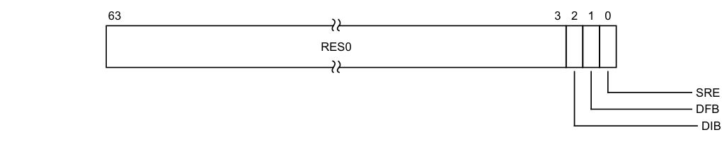
Image text
63 3 2 1 0
RES0
SRE
DFB
DIB
If EL3 is implemented and GICD_CTLR.DS == 1, and EL2 is not implemented, this field is a read-write alias of ICC_SRE_EL3.DIB.
If EL3 is not implemented and EL2 is implemented, this field is a read-only alias of ICC_SRE_EL2.DIB.
If GICD_CTLR.DS == 1 and EL2 is implemented, this field is a read-only alias of ICC_SRE_EL2.DIB.
In systems that do not support IRQ bypass, this field is RAO/WI.
On a Warm reset, this field resets to 0.
DFB, bit [1]
Disable FIQ bypass. 0b0 FIQ bypass enabled. 0b1 FIQ bypass disabled. If EL3 is implemented and GICD_CTLR.DS == 0, this field is a read-only alias of ICC_SRE_EL3.DFB.
If EL3 is implemented and GICD_CTLR.DS == 1, and EL2 is not implemented, this field is a read-write alias of ICC_SRE_EL3.DFB.
If EL3 is not implemented and EL2 is implemented, this field is a read-only alias of ICC_SRE_EL2.DFB.
If GICD_CTLR.DS == 1 and EL2 is implemented, this field is a read-only alias of ICC_SRE_EL2.DFB.
In systems that do not support FIQ bypass, this field is RAO/WI.
On a Warm reset, this field resets to 0.
SRE, bit [0]
System Register Enable.
0b0 The memory-mapped interface must be used. Access at EL1 to any ICC_* System register other than ICC_SRE_EL1 is trapped to EL1.
0b1 The System register interface for the current Security state is enabled.
If software changes this bit from 1 to 0 in the Secure instance of this register, the results are UNPREDICTABLE.
If an implementation supports only a System register interface to the GIC CPU interface, this bit is RAO/WI.
If EL3 is implemented and ICC_SRE_EL3.SRE==0 the Secure copy of this bit is RAZ/WI. If ICC_SRE_EL3.SRE is changed from zero to one, the Secure copy of this bit becomes UNKNOWN.
If EL2 is implemented and ICC_SRE_EL2.SRE==0 the Non-secure copy of this bit is RAZ/WI. If ICC_SRE_EL2.SRE is changed from zero to one, the Non-secure copy of this bit becomes UNKNOWN.
If EL3 is implemented and ICC_SRE_EL3.SRE==0 the Non-secure copy of this bit is RAZ/WI. If ICC_SRE_EL3.SRE is changed from zero to one, the Non-secure copy of this bit becomes UNKNOWN.
GICv3 implementations that do not require GICv2 compatibility might choose to make this bit RAO/WI. The following options are supported:
-
The Non-secure copy of ICC_SRE_EL1.SRE can be RAO/WI if ICC_SRE_EL2.SRE is also RAO/WI. This means all Non-secure software, including VMs using only virtual interrupts, must access the GIC using System registers.
-
The Secure copy of ICC_SRE_EL1.SRE can be RAO/WI if ICC_SRE_EL3.SRE and ICC_SRE_EL2.SRE are also RAO/WI. This means that all Secure software must access the GIC using System registers and all Non-secure accesses to registers for physical interrupts must use System registers.
Note A VM using only virtual interrupts might still use memory-mapped access if the Non-secure copy of ICC_SRE_EL1.SRE is not RAO/WI.
On a Warm reset, this field resets to 0.
Accessing the ICC_SRE_EL1
Execution with ICC_SRE_EL1.SRE set to 0 might make some System registers UNKNOWN.
Accesses to this register use the following encodings in the System instruction encoding space:
MRS , ICC_SRE_EL1
| op0 | op1 | CRn | CRm | op2 |
|---|---|---|---|---|
| 0b11 | 0b000 | 0b1100 | 0b1100 | 0b101 |
if PSTATE.EL == EL0 then UNDEFINED;
elsif PSTATE.EL == EL1 then
    if Halted() && HaveEL(EL3) && EDSCR.SDD == '1' &&
    boolean IMPLEMENTATION_DEFINED "EL3 trap priority
when SDD == '1'" && ICC_SRE_EL3.Enable == '0' then UNDEFINED;
elsif EL2Enabled() && ICC_SRE_EL2.Enable == '0' then AArch64.SystemAccessTrap(EL2, 0x18);
elsif HaveEL(EL3) && ICC_SRE_EL3.Enable == '0' then
    if Halted() && EDSCR.SDD == '1' then UNDEFINED;
else AArch64.SystemAccessTrap(EL3, 0x18);
elsif HaveEL(EL3) then
    if SCR_EL3.NS == '0' then
        return ICC_SRE_EL1_S;
else return ICC_SRE_EL1_NS;
else return ICC_SRE_EL1;
elsif PSTATE.EL == EL2 then
    if Halted() && HaveEL(EL3) && EDSCR.SDD == '1' &&
    boolean IMPLEMENTATION_DEFINED "EL3 trap priority
when SDD == '1'" && ICC_SRE_EL3.Enable == '0' then UNDEFINED;
elsif HaveEL(EL3) && ICC_SRE_EL3.Enable == '0' then
    if Halted() && EDSCR.SDD == '1' then UNDEFINED;
else AArch64.SystemAccessTrap(EL3, 0x18);
elsif HaveEL(EL3) then
    if SCR_EL3.NS == '0' then
        return ICC_SRE_EL1_S;
else return ICC_SRE_EL1_NS;
else return ICC_SRE_EL1;
elsif PSTATE.EL == EL3 then
    if SCR_EL3.NS == '0' then
        return ICC_SRE_EL1_S;
else return ICC_SRE_EL1_NS;
MSR ICC_SRE_EL1,
| op0 | op1 | CRn | CRm | op2 |
|---|---|---|---|---|
| 0b11 | 0b000 | 0b1100 | 0b1100 | 0b101 |
if PSTATE.EL == EL0 then UNDEFINED;
elsif PSTATE.EL == EL1 then
    if Halted() && HaveEL(EL3) && EDSCR.SDD == '1' &&
    boolean IMPLEMENTATION_DEFINED "EL3 trap priority
when SDD == '1'" && ICC_SRE_EL3.Enable == '0' then
UNDEFINED;
elsif EL2Enabled() && ICC_SRE_EL2.Enable == '0'
    then AArch64.SystemAccessTrap(EL2, 0x18);
elsif HaveEL(EL3) && ICC_SRE_EL3.Enable == '0' then
if Halted() && EDSCR.SDD == '1' then UNDEFINED;
else AArch64.SystemAccessTrap(EL3, 0x18);
elsif HaveEL(EL3) then
    if SCR_EL3.NS == '0' then ICC_SRE_EL1_S = X[t];
else ICC_SRE_EL1_NS = X[t];
else ICC_SRE_EL1 = X[t];
elsif PSTATE.EL == EL2 then
    if Halted() && HaveEL(EL3) && EDSCR.SDD == '1' &&
    boolean IMPLEMENTATION_DEFINED "EL3 trap priority
when SDD == '1'" && ICC_SRE_EL3.Enable == '0' then UNDEFINED;
elsif HaveEL(EL3) && ICC_SRE_EL3.Enable == '0' then
    if Halted() && EDSCR.SDD == '1' then UNDEFINED;
else AArch64.SystemAccessTrap(EL3, 0x18);
elsif HaveEL(EL3) then
    if SCR_EL3.NS == '0' then ICC_SRE_EL1_S = X[t];
else ICC_SRE_EL1_NS = X[t];
else ICC_SRE_EL1 = X[t];
elsif PSTATE.EL == EL3 then
    if SCR_EL3.NS == '0' then ICC_SRE_EL1_S = X[t];
else ICC_SRE_EL1_NS = X[t];
12.2.23 ICC_SRE_EL2, Interrupt Controller System Register Enable register (EL2)
The ICC_SRE_EL2 characteristics are:
Purpose
Controls whether the System register interface or the memory-mapped interface to the GIC CPU interface is used for EL2.
Configurations
AArch64 System register ICC_SRE_EL2 is architecturally mapped to AArch32 System register ICC_HSRE.
If EL2 is not implemented, this register is RES0 from EL3.
This register has no effect if EL2 is not enabled in the current Security state.
Attributes
ICC_SRE_EL2 is a 64-bit register.
Field descriptions
The ICC_SRE_EL2 bit assignments are:

Image text
63 4 3 2 1 0
RES0
SRE
DFB
DIB
Enable
Enable, bit [3]
Enable. Enables lower Exception level access to ICC_SRE_EL1.
0b0 When EL2 is implemented and enabled in the current Security state, EL1 accesses to ICC_SRE_EL1 trap to EL2.
0b1 EL1 accesses to ICC_SRE_EL1 do not trap to EL2. If ICC_SRE_EL2.SRE is RAO/WI, an implementation is permitted to make the Enable bit RAO/WI.
If ICC_SRE_EL2.SRE is 0, the Enable bit behaves as 1 for all purposes other than reading the value of the bit.
On a Warm reset, this field resets to an architecturally UNKNOWN value.
DIB, bit [2]
Disable IRQ bypass. 0b0 IRQ bypass enabled. 0b1 IRQ bypass disabled. If EL3 is implemented and GICD_CTLR.DS is 0, this field is a read-only alias of ICC_SRE_EL3.DIB. If EL3 is implemented and GICD_CTLR.DS is 1, this field is a read-write alias of ICC_SRE_EL3.DIB. In systems that do not support IRQ bypass, this bit is RAO/WI. On a Warm reset, this field resets to 0.
DFB, bit [1]
Disable FIQ bypass.
0b0 FIQ bypass enabled. 0b1 FIQ bypass disabled. If EL3 is implemented and GICD_CTLR.DS is 0, this field is a read-only alias of ICC_SRE_EL3.DFB.
If EL3 is implemented and GICD_CTLR.DS is 1, this field is a read-write alias of ICC_SRE_EL3.DFB.
In systems that do not support FIQ bypass, this bit is RAO/WI.
On a Warm reset, this field resets to 0.
SRE, bit [0]
System Register Enable.
0b0 The memory-mapped interface must be used. Access at EL2 to any ICH_* or ICC_* register other than ICC_SRE_EL1 or ICC_SRE_EL2, is trapped to EL2.
0b1 The System register interface to the ICH_* registers and the EL1 and EL2 ICC_* registers is enabled for EL2.
If software changes this bit from 1 to 0, the results are UNPREDICTABLE.
If an implementation supports only a System register interface to the GIC CPU interface, this bit is RAO/WI.
If EL3 is implemented and ICC_SRE_EL3.SRE==0 this bit is RAZ/WI. If ICC_SRE_EL3.SRE is changed from zero to one, this bit becomes UNKNOWN.
FEAT_GICv3 implementations that do not require GICv2 compatibility might choose to make this bit RAO/WI, but this is only allowed if ICC_SRE_EL3.SRE is also RAO/WI.
On a Warm reset, this field resets to 0.
Accessing the ICC_SRE_EL2
Execution with ICC_SRE_EL2.SRE set to 0 might make some System registers UNKNOWN.
Accesses to this register use the following encodings in the System instruction encoding space:
MRS , ICC_SRE_EL2
| op0 | op1 | CRn | CRm | op2 |
|---|---|---|---|---|
| 0b11 | 0b100 | 0b1100 | 0b1001 | 0b101 |
if PSTATE.EL == EL0 then UNDEFINED;
elsif PSTATE.EL == EL1 then
    if EL2Enabled() && HCR_EL2.NV == '1' then AArch64.SystemAccessTrap(EL2, 0x18);
else UNDEFINED;
elsif PSTATE.EL == EL2 then
    if Halted() && HaveEL(EL3) && EDSCR.SDD == '1' &&
    boolean IMPLEMENTATION_DEFINED "EL3 trap priority
when SDD == '1'" && ICC_SRE_EL3.Enable == '0' then
UNDEFINED;
elsif HaveEL(EL3) && ICC_SRE_EL3.Enable == '0'
    then if Halted() && EDSCR.SDD == '1'
    then UNDEFINED;
else AArch64.SystemAccessTrap(EL3, 0x18);
else
    return ICC_SRE_EL2;
elsif PSTATE.EL == EL3
    then if !EL2Enabled()
    then
UNDEFINED;
else
    return ICC_SRE_EL2;
MSR ICC_SRE_EL2,
| op0 | op1 | CRn | CRm | op2 |
|---|---|---|---|---|
| 0b11 | 0b100 | 0b1100 | 0b1001 | 0b101 |
if PSTATE.EL == EL0 then UNDEFINED;
elsif PSTATE.EL == EL1 then
    if EL2Enabled() && HCR_EL2.NV == '1' then AArch64.SystemAccessTrap(EL2, 0x18);
else UNDEFINED;
elsif PSTATE.EL == EL2 then
    if Halted() && HaveEL(EL3) && EDSCR.SDD == '1' &&
    boolean IMPLEMENTATION_DEFINED "EL3 trap priority
when SDD == '1'" && ICC_SRE_EL3.Enable == '0' then UNDEFINED;
elsif HaveEL(EL3) && ICC_SRE_EL3.Enable == '0' then
    if Halted() && EDSCR.SDD == '1' then UNDEFINED;
else AArch64.SystemAccessTrap(EL3, 0x18);
else ICC_SRE_EL2 = X[t];
elsif PSTATE.EL == EL3 then
    if !EL2Enabled() then UNDEFINED;
else ICC_SRE_EL2 = X[t];
12.2.24 ICC_SRE_EL3, Interrupt Controller System Register Enable register (EL3)
The ICC_SRE_EL3 characteristics are:
Purpose
Controls whether the System register interface or the memory-mapped interface to the GIC CPU interface is used for EL3.
Configurations
AArch64 System register ICC_SRE_EL3 bits [31:0] can be mapped to AArch32 System register ICC_MSRE[31:0], but this is not architecturally mandated.
This register is present only when EL3 is implemented. Otherwise, direct accesses to ICC_SRE_EL3 are UNDEFINED.
Attributes
ICC_SRE_EL3 is a 64-bit register.
Field descriptions
The ICC_SRE_EL3 bit assignments are:
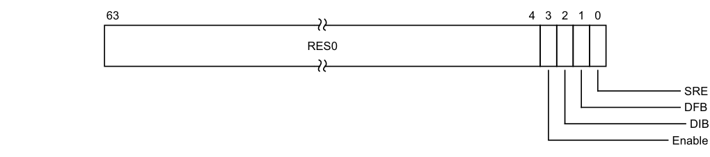
Image text
63 4 3 2 1 0
RES0
SRE
DFB
DIB
Enable
Enable, bit [3]
Enable. Enables lower Exception level access to ICC_SRE_EL1 and ICC_SRE_EL2.
0b0 EL1 accesses to ICC_SRE_EL1 trap to EL3, unless these accesses are trapped to EL2 as a result of ICC_SRE_EL2.Enable == 0. EL2 accesses to ICC_SRE_EL1 and ICC_SRE_EL2 trap to EL3. 0b1 EL1 accesses to ICC_SRE_EL1 do not trap to EL3.
EL2 accesses to ICC_SRE_EL1 and ICC_SRE_EL2 do not trap to EL3.
If ICC_SRE_EL3.SRE is RAO/WI, an implementation is permitted to make the Enable bit RAO/WI.
If ICC_SRE_EL3.SRE is 0, the Enable bit behaves as 1 for all purposes other than reading the value of the bit.
On a Warm reset, this field resets to an architecturally UNKNOWN value.
DIB, bit [2]
Disable IRQ bypass.
0b0 IRQ bypass enabled. 0b1 IRQ bypass disabled.
In systems that do not support IRQ bypass, this bit is RAO/WI.
On a Warm reset, this field resets to 0.
DFB, bit [1]
Disable FIQ bypass. 0b0 FIQ bypass enabled. 0b1 FIQ bypass disabled.
In systems that do not support FIQ bypass, this bit is RAO/WI.
On a Warm reset, this field resets to 0.
SRE, bit [0]
System Register Enable.
0b0 The memory-mapped interface must be used. Access at EL3 to any ICH_* or ICC_* register other than ICC_SRE_EL1, ICC_SRE_EL2, or ICC_SRE_EL3 is trapped to EL3
0b1 The System register interface to the ICH_* registers and the EL1, EL2, and EL3 ICC_* registers is enabled for EL3.
If software changes this bit from 1 to 0, the results are UNPREDICTABLE.
FEAT_GICv3 implementations that do not require GICv2 compatibility might choose to make this bit RAO/WI.
On a Warm reset, this field resets to 0.
Accessing the ICC_SRE_EL3
This register is always System register accessible.
Accesses to this register use the following encodings in the System instruction encoding space:
MRS , ICC_SRE_EL3
| op0 | op1 | CRn | CRm | op2 |
|---|---|---|---|---|
| 0b11 | 0b110 | 0b1100 | 0b1100 | 0b101 |
if PSTATE.EL == EL0
    then
UNDEFINED;
elsif PSTATE.EL == EL1
    then
UNDEFINED;
elsif PSTATE.EL == EL2
    then
UNDEFINED;
elsif PSTATE.EL == EL3
    then return ICC_SRE_EL3;
MSR ICC_SRE_EL3,
| op0 | op1 | CRn | CRm | op2 |
|---|---|---|---|---|
| 0b11 | 0b110 | 0b1100 | 0b1100 | 0b101 |
if PSTATE.EL == EL0
    then
UNDEFINED;
elsif PSTATE.EL == EL1
    then
UNDEFINED;
elsif PSTATE.EL == EL2
    then
UNDEFINED;
elsif PSTATE.EL == EL3
    then ICC_SRE_EL3 = X[t];
12.3 AArch64 System register descriptions of the virtual registers
This section describes each of the virtual AArch64 GIC System registers in register name order. The ICV prefix indicates a virtual GIC CPU interface System register. Each AArch64 System register description contains a reference to the AArch32 register that provides the same functionality.
Unless otherwise stated, the bit assignments for the GIC System registers are the same as those for the equivalent GICC_* and GICV_* memory-mapped registers.
The ICV_* registers are only accessible at EL1, and only if EL2 is enabled for the current Security state. Whether an access encoding maps to an ICC_* register or the equivalent ICV_* register is determined by HCR_EL2, see Chapter 6 Virtual Interrupt Handling and Prioritization . The equivalent virtual interface memory-mapped registers are described in The GIC virtual CPU interface register descriptions.
The encodings for the virtual registers are the same as for the physical registers, see Table 12-21.
12.3.1 ICV_AP0R_EL1, Interrupt Controller Virtual Active Priorities Group 0 Registers, n = 0 - 3
The ICV_AP0R
Purpose
Provides information about virtual Group 0 active priorities.
Configurations
AArch64 System register ICV_AP0R
Attributes
ICV_AP0R
Field descriptions
The ICV_AP0R

63 32 31 0
RES0 IMPLEMENTATION DEFINED
Bits [63:32]
Reserved, RES0.
IMPLEMENTATION DEFINED, bits [31:0]
IMPLEMENTATION DEFINED.
On a Warm reset, this field resets to an architecturally UNKNOWN value.
The contents of these registers are IMPLEMENTATION DEFINED with the one architectural requirement that the value 0x00000000 is consistent with no interrupts being active.
Accessing the ICV_AP0R_EL1
Writing to these registers with any value other than the last read value of the register (or 0x00000000 when there are no Group 0 active priorities) might result in UNPREDICTABLE behavior of the virtual interrupt prioritization system, causing:
-
Interrupts that should preempt execution to not preempt execution.
-
Interrupts that should not preempt execution to preempt execution.
ICV_AP0R1_EL1 is only implemented in implementations that support 6 or more bits of priority.
ICV_AP0R2_EL1 and ICV_AP0R3_EL1 are only implemented in implementations that support 7 bits of priority. Unimplemented registers are UNDEFINED.
Writing to the active priority registers in any order other than the following order might result in UNPREDICTABLE behavior of the interrupt prioritization system:
-
ICV_AP0R
_EL1. -
ICV_AP1R
_EL1.
Accesses to this register use the following encodings in the System instruction encoding space:
MRS , ICC_AP0R_EL1
| op0 | op1 | CRn | CRm | op2 |
|---|---|---|---|---|
| 0b11 | 0b000 | 0b1100 | 0b1000 | 0b1:n[1:0] |
if PSTATE.EL == EL0 then UNDEFINED;
elsif PSTATE.EL == EL1 then
    if Halted() && HaveEL(EL3) && EDSCR.SDD == '1' &&
    boolean IMPLEMENTATION_DEFINED "EL3 trap priority
when SDD == '1'" && SCR_EL3.FIQ == '1' then UNDEFINED;
elsif ICC_SRE_EL1.SRE == '0' then AArch64.SystemAccessTrap(EL1, 0x18);
elsif EL2Enabled() && ICH_HCR_EL2.TALL0 == '1' then AArch64.SystemAccessTrap(EL2, 0x18);
elsif EL2Enabled() && HCR_EL2.FMO == '1' then
    return ICV_AP0R_EL1[UInt(op2<1:0>)];
elsif HaveEL(EL3) && SCR_EL3.FIQ == '1' then
    if Halted() && EDSCR.SDD == '1' then UNDEFINED;
else AArch64.SystemAccessTrap(EL3, 0x18);
else return ICC_AP0R_EL1[UInt(op2<1:0>)];
elsif PSTATE.EL == EL2 then
    if Halted() && HaveEL(EL3) && EDSCR.SDD == '1' &&
    boolean IMPLEMENTATION_DEFINED "EL3 trap priority
when SDD == '1'" && SCR_EL3.FIQ == '1' then
UNDEFINED;
elsif ICC_SRE_EL2.SRE == '0'
    then AArch64.SystemAccessTrap(EL2, 0x18);
elsif HaveEL(EL3) && SCR_EL3.FIQ == '1'
    then if Halted() && EDSCR.SDD == '1'
    then UNDEFINED;
else AArch64.SystemAccessTrap(EL3, 0x18);
else return ICC_AP0R_EL1[UInt(op2<1:0>)];
elsif PSTATE.EL == EL3
    then if ICC_SRE_EL3.SRE == '0'
    then AArch64.SystemAccessTrap(EL3, 0x18);
else return ICC_AP0R_EL1[UInt(op2<1:0>)];
MSR ICC_AP0R_EL1,
| op0 | op1 | CRn | CRm | op2 |
|---|---|---|---|---|
| 0b11 | 0b000 | 0b1100 | 0b1000 | 0b1:n[1:0] |
if PSTATE.EL == EL0 then UNDEFINED;
elsif PSTATE.EL == EL1 then
    if Halted() && HaveEL(EL3) && EDSCR.SDD == '1' &&
    boolean IMPLEMENTATION_DEFINED "EL3 trap priority
when SDD == '1'" && SCR_EL3.FIQ == '1' then
UNDEFINED;
elsif ICC_SRE_EL1.SRE == '0'
    then AArch64.SystemAccessTrap(EL1, 0x18);
elsif EL2Enabled() && ICH_HCR_EL2.TALL0 == '1'
    then AArch64.SystemAccessTrap(EL2, 0x18);
elsif EL2Enabled() && HCR_EL2.FMO == '1'
    then ICV_AP0R_EL1[UInt(op2<1:0>)] = X[t];
elsif HaveEL(EL3) && SCR_EL3.FIQ == '1' then
if Halted() && EDSCR.SDD == '1' then UNDEFINED;
else AArch64.SystemAccessTrap(EL3, 0x18);
else ICC_AP0R_EL1[UInt(op2<1:0>)] = X[t];
elsif PSTATE.EL == EL2 then
    if Halted() && HaveEL(EL3) && EDSCR.SDD == '1' &&
    boolean IMPLEMENTATION_DEFINED "EL3 trap priority
when SDD == '1'" && SCR_EL3.FIQ == '1' then UNDEFINED;
elsif ICC_SRE_EL2.SRE == '0' then AArch64.SystemAccessTrap(EL2, 0x18);
elsif HaveEL(EL3) && SCR_EL3.FIQ == '1' then
    if Halted() && EDSCR.SDD == '1' then UNDEFINED;
else AArch64.SystemAccessTrap(EL3, 0x18);
else ICC_AP0R_EL1[UInt(op2<1:0>)] = X[t];
elsif PSTATE.EL == EL3 then
    if ICC_SRE_EL3.SRE == '0' then AArch64.SystemAccessTrap(EL3, 0x18);
else ICC_AP0R_EL1[UInt(op2<1:0>)] = X[t];
12.3.2 ICV_AP1R_EL1, Interrupt Controller Virtual Active Priorities Group 1 Registers, n = 0 - 3
The ICV_AP1R
Purpose
Provides information about virtual Group 1 active priorities.
Configurations
AArch64 System register ICV_AP1R
Attributes
ICV_AP1R
Field descriptions
The ICV_AP1R

63 32 31 0
RES0 IMPLEMENTATION DEFINED
Bits [63:32]
Reserved, RES0.
IMPLEMENTATION DEFINED, bits [31:0]
IMPLEMENTATION DEFINED.
On a Warm reset, this field resets to an architecturally UNKNOWN value.
The contents of these registers are IMPLEMENTATION DEFINED with the one architectural requirement that the value 0x00000000 is consistent with no interrupts being active.
Accessing the ICV_AP1R_EL1
Writing to these registers with any value other than the last read value of the register (or 0x00000000 when there are no Group 1 active priorities) might result in UNPREDICTABLE behavior of the virtual interrupt prioritization system, causing:
-
Interrupts that should preempt execution to not preempt execution.
-
Interrupts that should not preempt execution to preempt execution.
ICV_AP1R1_EL1 is only implemented in implementations that support 6 or more bits of priority.
ICV_AP1R2_EL1 and ICV_AP1R3_EL1 are only implemented in implementations that support 7 bits of priority. Unimplemented registers are UNDEFINED.
Writing to the active priority registers in any order other than the following order might result in UNPREDICTABLE behavior of the interrupt prioritization system:
-
ICV_AP0R
_EL1. -
ICV_AP1R
_EL1.
Accesses to this register use the following encodings in the System instruction encoding space:
MRS , ICC_AP1R_EL1
| op0 | op1 | CRn | CRm | op2 |
|---|---|---|---|---|
| 0b11 | 0b000 | 0b1100 | 0b1001 | 0b0:n[1:0] |
if PSTATE.EL == EL0 then UNDEFINED;
elsif PSTATE.EL == EL1 then
    if Halted() && HaveEL(EL3) && EDSCR.SDD == '1' &&
    boolean IMPLEMENTATION_DEFINED "EL3 trap priority
when SDD == '1'" && SCR_EL3.IRQ == '1' then UNDEFINED;
elsif ICC_SRE_EL1.SRE == '0' then AArch64.SystemAccessTrap(EL1, 0x18);
elsif EL2Enabled() && ICH_HCR_EL2.TALL1 == '1' then AArch64.SystemAccessTrap(EL2, 0x18);
elsif EL2Enabled() && HCR_EL2.IMO == '1' then
    return ICV_AP1R_EL1[UInt(op2<1:0>)];
elsif HaveEL(EL3) && SCR_EL3.IRQ == '1' then
    if Halted() && EDSCR.SDD == '1' then UNDEFINED;
else AArch64.SystemAccessTrap(EL3, 0x18);
elsif HaveEL(EL3) then
    if SCR_EL3.NS == '0' then
        return ICC_AP1R_EL1_S[UInt(op2<1:0>)];
else return ICC_AP1R_EL1_NS[UInt(op2<1:0>)];
else return ICC_AP1R_EL1[UInt(op2<1:0>)];
elsif PSTATE.EL == EL2 then
    if Halted() && HaveEL(EL3) && EDSCR.SDD == '1' &&
    boolean IMPLEMENTATION_DEFINED "EL3 trap priority
when SDD == '1'" && SCR_EL3.IRQ == '1' then UNDEFINED;
elsif ICC_SRE_EL2.SRE == '0' then AArch64.SystemAccessTrap(EL2, 0x18);
elsif HaveEL(EL3) && SCR_EL3.IRQ == '1' then
    if Halted() && EDSCR.SDD == '1' then UNDEFINED;
else AArch64.SystemAccessTrap(EL3, 0x18);
elsif HaveEL(EL3) then
    if SCR_EL3.NS == '0' then
        return ICC_AP1R_EL1_S[UInt(op2<1:0>)];
else return ICC_AP1R_EL1_NS[UInt(op2<1:0>)];
else return ICC_AP1R_EL1[UInt(op2<1:0>)];
elsif PSTATE.EL == EL3 then
    if ICC_SRE_EL3.SRE == '0' then AArch64.SystemAccessTrap(EL3, 0x18);
else if SCR_EL3.NS == '0' then
    return ICC_AP1R_EL1_S[UInt(op2<1:0>)];
else return ICC_AP1R_EL1_NS[UInt(op2<1:0>)];
MSR ICC_AP1R_EL1,
| op0 | op1 | CRn | CRm | op2 |
|---|---|---|---|---|
| 0b11 | 0b000 | 0b1100 | 0b1001 | 0b0:n[1:0] |
if PSTATE.EL == EL0 then UNDEFINED;
elsif PSTATE.EL == EL1 then
    if Halted() && HaveEL(EL3) && EDSCR.SDD == '1' &&
    boolean IMPLEMENTATION_DEFINED "EL3 trap priority
when SDD == '1'" && SCR_EL3.IRQ == '1' then UNDEFINED;
elsif ICC_SRE_EL1.SRE == '0' then AArch64.SystemAccessTrap(EL1, 0x18);
elsif EL2Enabled() && ICH_HCR_EL2.TALL1 == '1' then AArch64.SystemAccessTrap(EL2, 0x18);
elsif EL2Enabled() && HCR_EL2.IMO == '1' then ICV_AP1R_EL1[UInt(op2<1:0>)] = X[t];
elsif HaveEL(EL3) && SCR_EL3.IRQ == '1' then
    if Halted() && EDSCR.SDD == '1' then UNDEFINED;
else AArch64.SystemAccessTrap(EL3, 0x18);
elsif HaveEL(EL3) then
    if SCR_EL3.NS == '0' then ICC_AP1R_EL1_S[UInt(op2<1:0>)] = X[t];
else ICC_AP1R_EL1_NS[UInt(op2<1:0>)] = X[t];
else ICC_AP1R_EL1[UInt(op2<1:0>)] = X[t];
elsif PSTATE.EL == EL2 then
    if Halted() && HaveEL(EL3) && EDSCR.SDD == '1' &&
    boolean IMPLEMENTATION_DEFINED "EL3 trap priority
when SDD == '1'" && SCR_EL3.IRQ == '1' then UNDEFINED;
elsif ICC_SRE_EL2.SRE == '0' then AArch64.SystemAccessTrap(EL2, 0x18);
elsif HaveEL(EL3) && SCR_EL3.IRQ == '1' then
    if Halted() && EDSCR.SDD == '1' then UNDEFINED;
else AArch64.SystemAccessTrap(EL3, 0x18);
elsif HaveEL(EL3) then
    if SCR_EL3.NS == '0' then ICC_AP1R_EL1_S[UInt(op2<1:0>)] = X[t];
else ICC_AP1R_EL1_NS[UInt(op2<1:0>)] = X[t];
else ICC_AP1R_EL1[UInt(op2<1:0>)] = X[t];
elsif PSTATE.EL == EL3 then
    if ICC_SRE_EL3.SRE == '0' then AArch64.SystemAccessTrap(EL3, 0x18);
else if SCR_EL3.NS == '0' then ICC_AP1R_EL1_S[UInt(op2<1:0>)] = X[t];
else ICC_AP1R_EL1_NS[UInt(op2<1:0>)] = X[t];
12.3.3 ICV_BPR0_EL1, Interrupt Controller Virtual Binary Point Register 0
The ICV_BPR0_EL1 characteristics are:
Purpose
Defines the point at which the priority value fields split into two parts, the group priority field and the subpriority field. The group priority field determines virtual Group 0 interrupt preemption.
Configurations
AArch64 System register ICV_BPR0_EL1 bits [31:0] are architecturally mapped to AArch32 System register ICV_BPR0[31:0].
Attributes
ICV_BPR0_EL1 is a 64-bit register.
Field descriptions
The ICV_BPR0_EL1 bit assignments are:

63 3 2 0
RES0
BinaryPoint
Bits [63:3]
Reserved, RES0.
BinaryPoint, bits [2:0]
The value of this field controls how the 8-bit interrupt priority field is split into a group priority field, that determines interrupt preemption, and a subpriority field. This is done as follows:
| Binary point value | Group priority field | Subpriority field | Field with binary point |
|---|---|---|---|
| 0 | [7:1] | [0] | ggggggg.s |
| 1 | [7:2] | [1:0] | gggggg.ss |
| 2 | [7:3] | [2:0] | ggggg.sss |
| 3 | [7:4] | [3:0] | gggg.ssss |
| 4 | [7:5] | [4:0] | ggg.sssss |
| 5 | [7:6] | [5:0] | gg.ssssss |
| 6 | [7] | [6:0] | g.sssssss |
| 7 | No preemption | [7:0] | .ssssssss |
On a Warm reset, this field resets to an architecturally UNKNOWN value.
Accessing the ICV_BPR0_EL1
The minimum binary point value is derived from the number of implemented preemption bits, as shown in the following table:
| Number of implemented preemption bits | Minimum value of BPR0 |
|---|---|
| 7 | 0 |
| 6 | 1 |
| 5 | 2 |
The number of implemented preemption bits is indicated by ICH_VTR_EL2.PREbits.
An attempt to program the binary point field to a value less than the minimum value sets the field to the minimum value. On a reset, the binary point field is UNKNOWN.
Accesses to this register use the following encodings in the System instruction encoding space:
MRS , ICC_BPR0_EL1
| op0 | op1 | CRn | CRm | op2 |
|---|---|---|---|---|
| 0b11 | 0b000 | 0b1100 | 0b1000 | 0b011 |
if PSTATE.EL == EL0 then UNDEFINED;
elsif PSTATE.EL == EL1 then
    if Halted() && HaveEL(EL3) && EDSCR.SDD == '1' &&
    boolean IMPLEMENTATION_DEFINED "EL3 trap priority
when SDD == '1'" && SCR_EL3.FIQ == '1' then
UNDEFINED;
elsif ICC_SRE_EL1.SRE == '0'
    then AArch64.SystemAccessTrap(EL1, 0x18);
elsif EL2Enabled() && ICH_HCR_EL2.TALL0 == '1'
    then AArch64.SystemAccessTrap(EL2, 0x18);
elsif EL2Enabled() && HCR_EL2.FMO == '1'
    then return ICV_BPR0_EL1;
elsif HaveEL(EL3) && SCR_EL3.FIQ == '1'
    then if Halted() && EDSCR.SDD == '1'
    then UNDEFINED;
else AArch64.SystemAccessTrap(EL3, 0x18);
else return ICC_BPR0_EL1;
elsif PSTATE.EL == EL2
    then if Halted() && HaveEL(EL3) && EDSCR.SDD == '1' && boolean IMPLEMENTATION_DEFINED "EL3 trap priority when SDD == '1'" && SCR_EL3.FIQ == '1'
    then UNDEFINED;
elsif ICC_SRE_EL2.SRE == '0'
    then AArch64.SystemAccessTrap(EL2, 0x18);
elsif HaveEL(EL3) && SCR_EL3.FIQ == '1'
    then if Halted() && EDSCR.SDD == '1'
    then UNDEFINED;
else AArch64.SystemAccessTrap(EL3, 0x18);
else return ICC_BPR0_EL1;
elsif PSTATE.EL == EL3
    then if ICC_SRE_EL3.SRE == '0'
    then AArch64.SystemAccessTrap(EL3, 0x18);
else return ICC_BPR0_EL1;
MSR ICC_BPR0_EL1,
| op0 | op1 | CRn | CRm | op2 |
|---|---|---|---|---|
| 0b11 | 0b000 | 0b1100 | 0b1000 | 0b011 |
if PSTATE.EL == EL0 then UNDEFINED;
elsif PSTATE.EL == EL1 then
    if Halted() && HaveEL(EL3) && EDSCR.SDD == '1' &&
    boolean IMPLEMENTATION_DEFINED "EL3 trap priority
when SDD == '1'" && SCR_EL3.FIQ == '1' then UNDEFINED;
elsif ICC_SRE_EL1.SRE == '0' then AArch64.SystemAccessTrap(EL1, 0x18);
elsif EL2Enabled() && ICH_HCR_EL2.TALL0 == '1' then AArch64.SystemAccessTrap(EL2, 0x18);
elsif EL2Enabled() && HCR_EL2.FMO == '1' then ICV_BPR0_EL1 = X[t];
elsif HaveEL(EL3) && SCR_EL3.FIQ == '1' then
    if Halted() && EDSCR.SDD == '1' then UNDEFINED;
else AArch64.SystemAccessTrap(EL3, 0x18);
else ICC_BPR0_EL1 = X[t];
elsif PSTATE.EL == EL2 then
    if Halted() && HaveEL(EL3) && EDSCR.SDD == '1' &&
    boolean IMPLEMENTATION_DEFINED "EL3 trap priority
when SDD == '1'" && SCR_EL3.FIQ == '1' then UNDEFINED;
elsif ICC_SRE_EL2.SRE == '0' then AArch64.SystemAccessTrap(EL2, 0x18);
elsif HaveEL(EL3) && SCR_EL3.FIQ == '1' then
    if Halted() && EDSCR.SDD == '1' then UNDEFINED;
else AArch64.SystemAccessTrap(EL3, 0x18);
else ICC_BPR0_EL1 = X[t];
elsif PSTATE.EL == EL3 then
    if ICC_SRE_EL3.SRE == '0' then AArch64.SystemAccessTrap(EL3, 0x18);
else ICC_BPR0_EL1 = X[t];
12.3.4 ICV_BPR1_EL1, Interrupt Controller Virtual Binary Point Register 1
The ICV_BPR1_EL1 characteristics are:
Purpose
Defines the point at which the priority value fields split into two parts, the group priority field and the subpriority field. The group priority field determines virtual Group 1 interrupt preemption.
Configurations
AArch64 System register ICV_BPR1_EL1 bits [31:0] are architecturally mapped to AArch32 System register ICV_BPR1[31:0].
Attributes
ICV_BPR1_EL1 is a 64-bit register.
Field descriptions
The ICV_BPR1_EL1 bit assignments are:

63 3 2 0
RES0
BinaryPoint
Bits [63:3]
Reserved, RES0.
BinaryPoint, bits [2:0]
If the GIC is configured to use separate binary point fields for virtual Group 0 and virtual Group 1 interrupts, the value of this field controls how the 8-bit interrupt priority field is split into a group priority field, that determines interrupt preemption, and a subpriority field. This is done as follows:
Binary point value Group priority field Subpriority field Field with binary point
| 0 | - | - | - |
|---|---|---|---|
| 1 | [7:1] | [0] | ggggggg.s |
| 2 | [7:2] | [1:0] | gggggg.ss |
| 3 | [7:3] | [2:0] | ggggg.sss |
| 4 | [7:4] | [3:0] | gggg.ssss |
| 5 | [7:5] | [4:0] | ggg.sssss |
| 6 | [7:6] | [5:0] | gg.ssssss |
| 7 | [7] | [6:0] | g.sssssss |
Writing 0 to this field will set this field to its reset value.
If ICV_CTLR_EL1.CBPR is set to 1, Non-secure EL1 reads return ICV_BPR0_EL1 + 1 saturated to 0b111. Non-secure EL1 writes are ignored.
If ICV_CTLR_EL1.CBPR is set to 1, Secure EL1 reads return ICV_BPR0_EL1. Secure EL1 writes modify ICV_BPR0_EL1. On a Warm reset, this field resets to an architecturally UNKNOWN value.
Accessing the ICV_BPR1_EL1
For Non-secure writes, the minimum value of this field is the minimum value of ICH_VMCR_EL2.VBPR0 plus one.
For Secure writes, the minimum value of this field is the minimum value of ICH_VMCR_EL2.VBPR0.
An attempt to program the binary point field to a value less than the minimum value sets the field to the minimum value. On a reset, the binary point field is UNKNOWN.
Accesses to this register use the following encodings in the System instruction encoding space:
MRS , ICC_BPR1_EL1
| op0 | op1 | CRn | CRm | op2 |
|---|---|---|---|---|
| 0b11 | 0b000 | 0b1100 | 0b1100 | 0b011 |
if PSTATE.EL == EL0 then UNDEFINED;
elsif PSTATE.EL == EL1 then
    if Halted() && HaveEL(EL3) && EDSCR.SDD == '1' &&
    boolean IMPLEMENTATION_DEFINED "EL3 trap priority
when SDD == '1'" && SCR_EL3.IRQ == '1' then UNDEFINED;
elsif ICC_SRE_EL1.SRE == '0' then AArch64.SystemAccessTrap(EL1, 0x18);
elsif EL2Enabled() && ICH_HCR_EL2.TALL1 == '1' then AArch64.SystemAccessTrap(EL2, 0x18);
elsif EL2Enabled() && HCR_EL2.IMO == '1' then
    return ICV_BPR1_EL1;
elsif HaveEL(EL3) && SCR_EL3.IRQ == '1' then
    if Halted() && EDSCR.SDD == '1' then UNDEFINED;
else AArch64.SystemAccessTrap(EL3, 0x18);
elsif HaveEL(EL3) then
    if SCR_EL3.NS == '0' then
        return ICC_BPR1_EL1_S;
else return ICC_BPR1_EL1_NS;
else return ICC_BPR1_EL1;
elsif PSTATE.EL == EL2 then
    if Halted() && HaveEL(EL3) && EDSCR.SDD == '1' &&
    boolean IMPLEMENTATION_DEFINED "EL3 trap priority
when SDD == '1'" && SCR_EL3.IRQ == '1' then UNDEFINED;
elsif ICC_SRE_EL2.SRE == '0' then AArch64.SystemAccessTrap(EL2, 0x18);
elsif HaveEL(EL3) && SCR_EL3.IRQ == '1' then
    if Halted() && EDSCR.SDD == '1' then UNDEFINED;
else AArch64.SystemAccessTrap(EL3, 0x18);
elsif HaveEL(EL3) then
    if SCR_EL3.NS == '0' then
        return ICC_BPR1_EL1_S;
else return ICC_BPR1_EL1_NS;
else return ICC_BPR1_EL1;
elsif PSTATE.EL == EL3 then
    if ICC_SRE_EL3.SRE == '0' then AArch64.SystemAccessTrap(EL3, 0x18);
else if SCR_EL3.NS == '0' then
    return ICC_BPR1_EL1_S;
else return ICC_BPR1_EL1_NS;
MSR ICC_BPR1_EL1,
| op0 | op1 | CRn | CRm | op2 |
|---|---|---|---|---|
| 0b11 | 0b000 | 0b1100 | 0b1100 | 0b011 |
if PSTATE.EL == EL0 then UNDEFINED;
elsif PSTATE.EL == EL1 then
    if Halted() && HaveEL(EL3) && EDSCR.SDD == '1' &&
    boolean IMPLEMENTATION_DEFINED "EL3 trap priority
when SDD == '1'" && SCR_EL3.IRQ == '1' then UNDEFINED;
elsif ICC_SRE_EL1.SRE == '0' then AArch64.SystemAccessTrap(EL1, 0x18);
elsif EL2Enabled() && ICH_HCR_EL2.TALL1 == '1' then AArch64.SystemAccessTrap(EL2, 0x18);
elsif EL2Enabled() && HCR_EL2.IMO == '1' then ICV_BPR1_EL1 = X[t];
elsif HaveEL(EL3) && SCR_EL3.IRQ == '1' then
    if Halted() && EDSCR.SDD == '1' then UNDEFINED;
else AArch64.SystemAccessTrap(EL3, 0x18);
elsif HaveEL(EL3) then
    if SCR_EL3.NS == '0' then ICC_BPR1_EL1_S = X[t];
else ICC_BPR1_EL1_NS = X[t];
else ICC_BPR1_EL1 = X[t];
elsif PSTATE.EL == EL2 then
    if Halted() && HaveEL(EL3) && EDSCR.SDD == '1' &&
    boolean IMPLEMENTATION_DEFINED "EL3 trap priority
when SDD == '1'" && SCR_EL3.IRQ == '1' then UNDEFINED;
elsif ICC_SRE_EL2.SRE == '0' then AArch64.SystemAccessTrap(EL2, 0x18);
elsif HaveEL(EL3) && SCR_EL3.IRQ == '1' then
    if Halted() && EDSCR.SDD == '1' then UNDEFINED;
else AArch64.SystemAccessTrap(EL3, 0x18);
elsif HaveEL(EL3) then
    if SCR_EL3.NS == '0' then ICC_BPR1_EL1_S = X[t];
else ICC_BPR1_EL1_NS = X[t];
else ICC_BPR1_EL1 = X[t];
elsif PSTATE.EL == EL3 then
    if ICC_SRE_EL3.SRE == '0' then AArch64.SystemAccessTrap(EL3, 0x18);
else if SCR_EL3.NS == '0' then ICC_BPR1_EL1_S = X[t];
else ICC_BPR1_EL1_NS = X[t];
12.3.5 ICV_CTLR_EL1, Interrupt Controller Virtual Control Register
The ICV_CTLR_EL1 characteristics are:
Purpose
Controls aspects of the behavior of the GIC virtual CPU interface and provides information about the features implemented.
Configurations
AArch64 System register ICV_CTLR_EL1 bits [31:0] are architecturally mapped to AArch32 System register ICV_CTLR[31:0].
Attributes
ICV_CTLR_EL1 is a 64-bit register.
Field descriptions
The ICV_CTLR_EL1 bit assignments are:
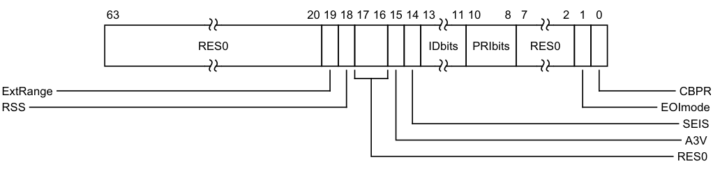
Image text
63 20 19 18 17 16 15 14 13 11 10 8 7 2 1 0
RES0 IDbits PRIbits RES0
ExtRange CBPR
RSS EOImode
SEIS
A3V
RES0
Reserved, RES0.
ExtRange, bit [19]
Extended INTID range (read-only).
-
0b0 CPU interface does not support INTIDs in the range 1024..8191.
- Behaviour is UNPREDICTABLE if the IRI delivers an interrupt in the range 1024 to 8191 to the CPU interface.
Note Arm strongly recommends that the IRI is not configured to deliver interrupts in this range to a PE that does not support them.
-
0b1 CPU interface supports INTIDs in the range 1024..8191
- All INTIDs in the range 1024..8191 are treated as requiring deactivation.
ICV_CTLR_EL1.ExtRange is an alias of ICC_CTLR_EL1.ExtRange.
RSS, bit [18]
Range Selector Support. Possible values are:
-
0b0 Targeted SGIs with affinity level 0 values of 0 - 15 are supported.
-
0b1 Targeted SGIs with affinity level 0 values of 0 - 255 are supported.
-
This bit is read-only.
Bits [17:16]
Reserved, RES0.
A3V, bit [15]
Affinity 3 Valid. Read-only and writes are ignored. Possible values are:
0b0 The virtual CPU interface logic only supports zero values of Affinity 3 in SGI generation System registers. 0b1 The virtual CPU interface logic supports non-zero values of Affinity 3 in SGI generation System registers.
SEIS, bit [14]
SEI Support. Read-only and writes are ignored. Indicates whether the virtual CPU interface supports local generation of SEIs:
0b0 The virtual CPU interface logic does not support local generation of SEIs. 0b1 The virtual CPU interface logic supports local generation of SEIs.
IDbits, bits [13:11]
Identifier bits. Read-only and writes are ignored. The number of virtual interrupt identifier bits supported:
0b000 16 bits. 0b001 24 bits. All other values are reserved.
PRIbits, bits [10:8]
Priority bits. Read-only and writes are ignored. The number of priority bits implemented, minus one.
An implementation must implement at least 32 levels of physical priority (5 priority bits).
Note This field always returns the number of priority bits implemented.
The division between group priority and subpriority is defined in the binary point registers ICV_BPR0_EL1 and ICV_BPR1_EL1.
Bits [7:2]
Reserved, RES0.
EOImode, bit [1]
Virtual EOI mode. Controls whether a write to an End of Interrupt register also deactivates the virtual interrupt:
0b0 ICV_EOIR0_EL1 and ICV_EOIR1_EL1 provide both priority drop and interrupt deactivation functionality. Accesses to ICV_DIR_EL1 are UNPREDICTABLE. 0b1 ICV_EOIR0_EL1 and ICV_EOIR1_EL1 provide priority drop functionality only. ICV_DIR_EL1 provides interrupt deactivation functionality.
On a Warm reset, this field resets to an architecturally UNKNOWN value.
CBPR, bit [0]
Common Binary Point Register. Controls whether the same register is used for interrupt preemption of both virtual Group 0 and virtual Group 1 interrupts:
0b0 ICV_BPR1_EL1 determines the preemption group for virtual Group 1 interrupts. 0b1 Reads of ICV_BPR1_EL1 return ICV_BPR0_EL1 plus one, saturated to 0b111. Writes to ICV_BPR1_EL1 are ignored.
On a Warm reset, this field resets to an architecturally UNKNOWN value.
Accessing the ICV_CTLR_EL1
Accesses to this register use the following encodings in the System instruction encoding space:
MRS , ICC_CTLR_EL1
| op0 | op1 | CRn | CRm | op2 |
|---|---|---|---|---|
| 0b11 | 0b000 | 0b1100 | 0b1100 | 0b100 |
if PSTATE.EL == EL0 then UNDEFINED;
elsif PSTATE.EL == EL1 then
    if Halted() && HaveEL(EL3) && EDSCR.SDD == '1' &&
    boolean IMPLEMENTATION_DEFINED "EL3 trap priority
when SDD == '1'" && SCR_EL3.<IRQ,FIQ> == '11' then UNDEFINED;
elsif ICC_SRE_EL1.SRE == '0' then AArch64.SystemAccessTrap(EL1, 0x18);
elsif EL2Enabled() && ICH_HCR_EL2.TC == '1' then AArch64.SystemAccessTrap(EL2, 0x18);
elsif EL2Enabled() && HCR_EL2.FMO == '1' then
    return ICV_CTLR_EL1;
elsif EL2Enabled() && HCR_EL2.IMO == '1' then
    return ICV_CTLR_EL1;
elsif HaveEL(EL3) && SCR_EL3.<IRQ,FIQ> == '11' then
    if Halted() && EDSCR.SDD == '1' then UNDEFINED;
else AArch64.SystemAccessTrap(EL3, 0x18);
elsif HaveEL(EL3) then
    if SCR_EL3.NS == '0' then
        return ICC_CTLR_EL1_S;
else return ICC_CTLR_EL1_NS;
else return ICC_CTLR_EL1;
elsif PSTATE.EL == EL2 then
    if Halted() && HaveEL(EL3) && EDSCR.SDD == '1' &&
    boolean IMPLEMENTATION_DEFINED "EL3 trap priority
when SDD == '1'" && SCR_EL3.<IRQ,FIQ> == '11' then UNDEFINED;
elsif ICC_SRE_EL2.SRE == '0' then AArch64.SystemAccessTrap(EL2, 0x18);
elsif HaveEL(EL3) && SCR_EL3.<IRQ,FIQ> == '11' then
    if Halted() && EDSCR.SDD == '1' then UNDEFINED;
else AArch64.SystemAccessTrap(EL3, 0x18);
elsif HaveEL(EL3) then
    if SCR_EL3.NS == '0' then
        return ICC_CTLR_EL1_S;
else return ICC_CTLR_EL1_NS;
else return ICC_CTLR_EL1;
elsif PSTATE.EL == EL3 then
    if ICC_SRE_EL3.SRE == '0' then AArch64.SystemAccessTrap(EL3, 0x18);
else if SCR_EL3.NS == '0' then
    return ICC_CTLR_EL1_S;
else return ICC_CTLR_EL1_NS;
MSR ICC_CTLR_EL1,
| op0 | op1 | CRn | CRm | op2 |
|---|---|---|---|---|
| 0b11 | 0b000 | 0b1100 | 0b1100 | 0b100 |
if PSTATE.EL == EL0 then UNDEFINED;
elsif PSTATE.EL == EL1 then
    if Halted() && HaveEL(EL3) && EDSCR.SDD == '1' &&
    boolean IMPLEMENTATION_DEFINED "EL3 trap priority
when SDD == '1'" && SCR_EL3.<IRQ,FIQ> == '11' then UNDEFINED;
elsif ICC_SRE_EL1.SRE == '0' then AArch64.SystemAccessTrap(EL1, 0x18);
elsif EL2Enabled() && ICH_HCR_EL2.TC == '1' then AArch64.SystemAccessTrap(EL2, 0x18);
elsif EL2Enabled() && HCR_EL2.FMO == '1' then ICV_CTLR_EL1 = X[t];
elsif EL2Enabled() && HCR_EL2.IMO == '1' then ICV_CTLR_EL1 = X[t];
elsif HaveEL(EL3) && SCR_EL3.<IRQ,FIQ> == '11' then
    if Halted() && EDSCR.SDD == '1' then UNDEFINED;
else AArch64.SystemAccessTrap(EL3, 0x18);
elsif HaveEL(EL3) then
    if SCR_EL3.NS == '0' then ICC_CTLR_EL1_S = X[t];
else ICC_CTLR_EL1_NS = X[t];
else ICC_CTLR_EL1 = X[t];
elsif PSTATE.EL == EL2 then
    if Halted() && HaveEL(EL3) && EDSCR.SDD == '1' &&
    boolean IMPLEMENTATION_DEFINED "EL3 trap priority
when SDD == '1'" && SCR_EL3.<IRQ,FIQ> == '11' then UNDEFINED;
elsif ICC_SRE_EL2.SRE == '0' then AArch64.SystemAccessTrap(EL2, 0x18);
elsif HaveEL(EL3) && SCR_EL3.<IRQ,FIQ> == '11' then
    if Halted() && EDSCR.SDD == '1' then UNDEFINED;
else AArch64.SystemAccessTrap(EL3, 0x18);
elsif HaveEL(EL3) then
    if SCR_EL3.NS == '0' then ICC_CTLR_EL1_S = X[t];
else ICC_CTLR_EL1_NS = X[t];
else ICC_CTLR_EL1 = X[t];
elsif PSTATE.EL == EL3 then
    if ICC_SRE_EL3.SRE == '0' then AArch64.SystemAccessTrap(EL3, 0x18);
else if SCR_EL3.NS == '0' then ICC_CTLR_EL1_S = X[t];
else ICC_CTLR_EL1_NS = X[t];
12.3.6 ICV_DIR_EL1, Interrupt Controller Deactivate Virtual Interrupt Register
The ICV_DIR_EL1 characteristics are:
Purpose
When interrupt priority drop is separated from interrupt deactivation, a write to this register deactivates the specified virtual interrupt.
Configurations
AArch64 System register ICV_DIR_EL1 bits [31:0] performs the same function as AArch32 System register ICV_DIR[31:0].
Attributes
ICV_DIR_EL1 is a 64-bit register.
Field descriptions
The ICV_DIR_EL1 bit assignments are:

63 24 23 0
RES0 INTID
Bits [63:24]
Reserved, RES0.
INTID, bits [23:0]
The INTID of the virtual interrupt to be deactivated.
This field has either 16 or 24 bits implemented. The number of implemented bits can be found in ICV_CTLR_EL1.IDbits. If only 16 bits are implemented, bits [23:16] of this register are RES0.
Accessing the ICV_DIR_EL1
When EOImode == 0, writes are ignored. In systems supporting system error generation, an implementation might generate an SEI.
Accesses to this register use the following encodings in the System instruction encoding space:
MSR ICC_DIR_EL1,
| op0 | op1 | CRn | CRm | op2 |
|---|---|---|---|---|
| 0b11 | 0b000 | 0b1100 | 0b1011 | 0b001 |
if PSTATE.EL == EL0 then UNDEFINED;
elsif PSTATE.EL == EL1 then
    if Halted() && HaveEL(EL3) && EDSCR.SDD == '1' &&
    boolean IMPLEMENTATION_DEFINED "EL3 trap priority
when SDD == '1'" && SCR_EL3.<IRQ,FIQ> == '11' then
UNDEFINED;
elsif ICC_SRE_EL1.SRE == '0'
    then AArch64.SystemAccessTrap(EL1, 0x18);
elsif EL2Enabled() && ICH_HCR_EL2.TDIR == '1'
    then AArch64.SystemAccessTrap(EL2, 0x18);
elsif EL2Enabled() && ICH_HCR_EL2.TC == '1'
    then AArch64.SystemAccessTrap(EL2, 0x18);
elsif EL2Enabled() && HCR_EL2.FMO == '1' then
ICV_DIR_EL1 = X[t];
elsif EL2Enabled() && HCR_EL2.IMO == '1'
    then ICV_DIR_EL1 = X[t];
elsif HaveEL(EL3) && SCR_EL3.<IRQ,FIQ> == '11'
    then if Halted() && EDSCR.SDD == '1'
    then UNDEFINED;
else AArch64.SystemAccessTrap(EL3, 0x18);
else ICC_DIR_EL1 = X[t];
elsif PSTATE.EL == EL2
    then if Halted() && HaveEL(EL3) && EDSCR.SDD == '1' && boolean IMPLEMENTATION_DEFINED "EL3 trap priority when SDD == '1'" && SCR_EL3.<IRQ,FIQ> == '11'
    then UNDEFINED;
elsif ICC_SRE_EL2.SRE == '0'
    then AArch64.SystemAccessTrap(EL2, 0x18);
elsif HaveEL(EL3) && SCR_EL3.<IRQ,FIQ> == '11'
    then if Halted() && EDSCR.SDD == '1'
    then UNDEFINED;
else AArch64.SystemAccessTrap(EL3, 0x18);
else ICC_DIR_EL1 = X[t];
elsif PSTATE.EL == EL3
    then if ICC_SRE_EL3.SRE == '0'
    then AArch64.SystemAccessTrap(EL3, 0x18);
else ICC_DIR_EL1 = X[t];
12.3.7 ICV_EOIR0_EL1, Interrupt Controller Virtual End Of Interrupt Register 0
The ICV_EOIR0_EL1 characteristics are:
Purpose
A PE writes to this register to inform the CPU interface that it has completed the processing of the specified virtual Group 0 interrupt.
Configurations
AArch64 System register ICV_EOIR0_EL1 performs the same function as AArch32 System register ICV_EOIR0.
Attributes
ICV_EOIR0_EL1 is a 64-bit register.
Field descriptions
The ICV_EOIR0_EL1 bit assignments are:

63 24 23 0
RES0 INTID
Bits [63:24]
Reserved, RES0.
INTID, bits [23:0]
The INTID from the corresponding ICV_IAR0_EL1 access.
This field has either 16 or 24 bits implemented. The number of implemented bits can be found in ICV_CTLR_EL1.IDbits. If only 16 bits are implemented, bits [23:16] of this register are RES0.
If the ICV_CTLR.EOImode bit is 0, a write to this register drops the priority for the virtual interrupt, and also deactivates the virtual interrupt.
If the ICV_CTLR.EOImode bit is 1, a write to this register only drops the priority for the virtual interrupt. Software must write to ICV_DIR_EL1 to deactivate the virtual interrupt.
Accessing the ICV_EOIR0_EL1
A write to this register must correspond to the most recent valid read by this vPE from a Virtual Interrupt Acknowledge Register, and must correspond to the INTID that was read from ICV_IAR0_EL1, otherwise the system behavior is UNPREDICTABLE. A valid read is a read that returns a valid INTID that is not a special INTID.
Accesses to this register use the following encodings in the System instruction encoding space:
MSR ICC_EOIR0_EL1,
| op0 | op1 | CRn | CRm | op2 |
|---|---|---|---|---|
| 0b11 | 0b000 | 0b1100 | 0b1000 | 0b001 |
if PSTATE.EL == EL0 then UNDEFINED;
elsif PSTATE.EL == EL1 then
    if Halted() && HaveEL(EL3) && EDSCR.SDD == '1' &&
    boolean IMPLEMENTATION_DEFINED "EL3 trap priority
when SDD == '1'" && SCR_EL3.FIQ == '1' then
UNDEFINED;
elsif ICC_SRE_EL1.SRE == '0' then
AArch64.SystemAccessTrap(EL1, 0x18);
elsif EL2Enabled() && ICH_HCR_EL2.TALL0 == '1'
    then AArch64.SystemAccessTrap(EL2, 0x18);
elsif EL2Enabled() && HCR_EL2.FMO == '1'
    then ICV_EOIR0_EL1 = X[t];
elsif HaveEL(EL3) && SCR_EL3.FIQ == '1'
    then if Halted() && EDSCR.SDD == '1'
    then UNDEFINED;
else AArch64.SystemAccessTrap(EL3, 0x18);
else ICC_EOIR0_EL1 = X[t];
elsif PSTATE.EL == EL2
    then if Halted() && HaveEL(EL3) && EDSCR.SDD == '1' && boolean IMPLEMENTATION_DEFINED "EL3 trap priority when SDD == '1'" && SCR_EL3.FIQ == '1'
    then UNDEFINED;
elsif ICC_SRE_EL2.SRE == '0'
    then AArch64.SystemAccessTrap(EL2, 0x18);
elsif HaveEL(EL3) && SCR_EL3.FIQ == '1'
    then if Halted() && EDSCR.SDD == '1'
    then UNDEFINED;
else AArch64.SystemAccessTrap(EL3, 0x18);
else ICC_EOIR0_EL1 = X[t];
elsif PSTATE.EL == EL3
    then if ICC_SRE_EL3.SRE == '0'
    then AArch64.SystemAccessTrap(EL3, 0x18);
else ICC_EOIR0_EL1 = X[t];
12.3.8 ICV_EOIR1_EL1, Interrupt Controller Virtual End Of Interrupt Register 1
The ICV_EOIR1_EL1 characteristics are:
Purpose
A PE writes to this register to inform the CPU interface that it has completed the processing of the specified virtual Group 1 interrupt.
Configurations
AArch64 System register ICV_EOIR1_EL1 performs the same function as AArch32 System register ICV_EOIR1.
Attributes
ICV_EOIR1_EL1 is a 64-bit register.
Field descriptions
The ICV_EOIR1_EL1 bit assignments are:

63 24 23 0
RES0 INTID
Bits [63:24]
Reserved, RES0.
INTID, bits [23:0]
The INTID from the corresponding ICV_IAR1_EL1 access.
This field has either 16 or 24 bits implemented. The number of implemented bits can be found in ICV_CTLR_EL1.IDbits. If only 16 bits are implemented, bits [23:16] of this register are RES0.
If the ICV_CTLR.EOImode bit is 0, a write to this register drops the priority for the virtual interrupt, and also deactivates the virtual interrupt.
If the ICV_CTLR.EOImode bit is 1, a write to this register only drops the priority for the virtual interrupt. Software must write to ICV_DIR_EL1 to deactivate the virtual interrupt.
Accessing the ICV_EOIR1_EL1
A write to this register must correspond to the most recent valid read by this vPE from a Virtual Interrupt Acknowledge Register, and must correspond to the INTID that was read from ICV_IAR1_EL1, otherwise the system behavior is UNPREDICTABLE. A valid read is a read that returns a valid INTID that is not a special INTID.
Accesses to this register use the following encodings in the System instruction encoding space:
MSR ICC_EOIR1_EL1,
| op0 | op1 | CRn | CRm | op2 |
|---|---|---|---|---|
| 0b11 | 0b000 | 0b1100 | 0b1100 | 0b001 |
if PSTATE.EL == EL0 then UNDEFINED;
elsif PSTATE.EL == EL1 then
    if Halted() && HaveEL(EL3) && EDSCR.SDD == '1' &&
    boolean IMPLEMENTATION_DEFINED "EL3 trap priority
when SDD == '1'" && SCR_EL3.IRQ == '1' then
UNDEFINED;
elsif ICC_SRE_EL1.SRE == '0' then
AArch64.SystemAccessTrap(EL1, 0x18);
elsif EL2Enabled() && ICH_HCR_EL2.TALL1 == '1'
    then AArch64.SystemAccessTrap(EL2, 0x18);
elsif EL2Enabled() && HCR_EL2.IMO == '1'
    then ICV_EOIR1_EL1 = X[t];
elsif HaveEL(EL3) && SCR_EL3.IRQ == '1'
    then if Halted() && EDSCR.SDD == '1'
    then UNDEFINED;
else AArch64.SystemAccessTrap(EL3, 0x18);
else ICC_EOIR1_EL1 = X[t];
elsif PSTATE.EL == EL2
    then if Halted() && HaveEL(EL3) && EDSCR.SDD == '1' && boolean IMPLEMENTATION_DEFINED "EL3 trap priority when SDD == '1'" && SCR_EL3.IRQ == '1'
    then UNDEFINED;
elsif ICC_SRE_EL2.SRE == '0'
    then AArch64.SystemAccessTrap(EL2, 0x18);
elsif HaveEL(EL3) && SCR_EL3.IRQ == '1'
    then if Halted() && EDSCR.SDD == '1'
    then UNDEFINED;
else AArch64.SystemAccessTrap(EL3, 0x18);
else ICC_EOIR1_EL1 = X[t];
elsif PSTATE.EL == EL3
    then if ICC_SRE_EL3.SRE == '0'
    then AArch64.SystemAccessTrap(EL3, 0x18);
else ICC_EOIR1_EL1 = X[t];
12.3.9 ICV_HPPIR0_EL1, Interrupt Controller Virtual Highest Priority Pending Interrupt Register 0
The ICV_HPPIR0_EL1 characteristics are:
Purpose
Indicates the highest priority pending virtual Group 0 interrupt on the virtual CPU interface.
Configurations
AArch64 System register ICV_HPPIR0_EL1 performs the same function as AArch32 System register ICV_HPPIR0.
Attributes
ICV_HPPIR0_EL1 is a 64-bit register.
Field descriptions
The ICV_HPPIR0_EL1 bit assignments are:
| | 63 | | 24 | 23 | | 0 | | |—|—|—|—|—|—|—| |||||||||
Bits [63:24]
Reserved, RES0.
INTID, bits [23:0]
The INTID of the highest priority pending virtual interrupt.
If the highest priority pending interrupt is not observable, this field contains a special INTID to indicate the reason. This special INTID can take the value 1023 only. For more information, see special interrupt.
This field has either 16 or 24 bits implemented. The number of implemented bits can be found in ICV_CTLR_EL1.IDbits. If only 16 bits are implemented, bits [23:16] of this register are RES0.
Accessing the ICV_HPPIR0_EL1
Accesses to this register use the following encodings in the System instruction encoding space:
MRS , ICC_HPPIR0_EL1
| op0 | op1 | CRn | CRm | op2 |
|---|---|---|---|---|
| 0b11 | 0b000 | 0b1100 | 0b1000 | 0b010 |
if PSTATE.EL == EL0 then UNDEFINED;
elsif PSTATE.EL == EL1 then
    if Halted() && HaveEL(EL3) && EDSCR.SDD == '1' &&
    boolean IMPLEMENTATION_DEFINED "EL3 trap priority
when SDD == '1'" && SCR_EL3.FIQ == '1' then
UNDEFINED;
elsif ICC_SRE_EL1.SRE == '0'
    then AArch64.SystemAccessTrap(EL1, 0x18);
elsif EL2Enabled() && ICH_HCR_EL2.TALL0 == '1'
    then AArch64.SystemAccessTrap(EL2, 0x18);
elsif EL2Enabled() && HCR_EL2.FMO == '1'
    then return ICV_HPPIR0_EL1;
elsif HaveEL(EL3) && SCR_EL3.FIQ == '1' then
if Halted() && EDSCR.SDD == '1' then UNDEFINED;
else AArch64.SystemAccessTrap(EL3, 0x18);
else return ICC_HPPIR0_EL1;
elsif PSTATE.EL == EL2 then
    if Halted() && HaveEL(EL3) && EDSCR.SDD == '1' &&
    boolean IMPLEMENTATION_DEFINED "EL3 trap priority
when SDD == '1'" && SCR_EL3.FIQ == '1' then UNDEFINED;
elsif ICC_SRE_EL2.SRE == '0' then AArch64.SystemAccessTrap(EL2, 0x18);
elsif HaveEL(EL3) && SCR_EL3.FIQ == '1' then
    if Halted() && EDSCR.SDD == '1' then UNDEFINED;
else AArch64.SystemAccessTrap(EL3, 0x18);
else return ICC_HPPIR0_EL1;
elsif PSTATE.EL == EL3 then
    if ICC_SRE_EL3.SRE == '0' then AArch64.SystemAccessTrap(EL3, 0x18);
else return ICC_HPPIR0_EL1;
12.3.10 ICV_HPPIR1_EL1, Interrupt Controller Virtual Highest Priority Pending Interrupt Register 1
The ICV_HPPIR1_EL1 characteristics are:
Purpose
Indicates the highest priority pending virtual Group 1 interrupt on the virtual CPU interface.
Configurations
AArch64 System register ICV_HPPIR1_EL1 performs the same function as AArch32 System register ICV_HPPIR1.
Attributes
ICV_HPPIR1_EL1 is a 64-bit register.
Field descriptions
The ICV_HPPIR1_EL1 bit assignments are:
| | 63 | | 24 | 23 | | 0 | | |—|—|—|—|—|—|—| |||||||||
Bits [63:24]
Reserved, RES0.
INTID, bits [23:0]
The INTID of the highest priority pending virtual interrupt.
If the highest priority pending interrupt is not observable, this field contains a special INTID to indicate the reason. This special INTID can take the value 1023 only. For more information, see special interrupt.
This field has either 16 or 24 bits implemented. The number of implemented bits can be found in ICV_CTLR_EL1.IDbits. If only 16 bits are implemented, bits [23:16] of this register are RES0.
Accessing the ICV_HPPIR1_EL1
Accesses to this register use the following encodings in the System instruction encoding space:
MRS , ICC_HPPIR1_EL1
| op0 | op1 | CRn | CRm | op2 |
|---|---|---|---|---|
| 0b11 | 0b000 | 0b1100 | 0b1100 | 0b010 |
if PSTATE.EL == EL0 then UNDEFINED;
elsif PSTATE.EL == EL1 then
    if Halted() && HaveEL(EL3) && EDSCR.SDD == '1' &&
    boolean IMPLEMENTATION_DEFINED "EL3 trap priority
when SDD == '1'" && SCR_EL3.IRQ == '1' then
UNDEFINED;
elsif ICC_SRE_EL1.SRE == '0'
    then AArch64.SystemAccessTrap(EL1, 0x18);
elsif EL2Enabled() && ICH_HCR_EL2.TALL1 == '1'
    then AArch64.SystemAccessTrap(EL2, 0x18);
elsif EL2Enabled() && HCR_EL2.IMO == '1'
    then return ICV_HPPIR1_EL1;
elsif HaveEL(EL3) && SCR_EL3.IRQ == '1' then
if Halted() && EDSCR.SDD == '1' then UNDEFINED;
else AArch64.SystemAccessTrap(EL3, 0x18);
else return ICC_HPPIR1_EL1;
elsif PSTATE.EL == EL2 then
    if Halted() && HaveEL(EL3) && EDSCR.SDD == '1' &&
    boolean IMPLEMENTATION_DEFINED "EL3 trap priority
when SDD == '1'" && SCR_EL3.IRQ == '1' then UNDEFINED;
elsif ICC_SRE_EL2.SRE == '0' then AArch64.SystemAccessTrap(EL2, 0x18);
elsif HaveEL(EL3) && SCR_EL3.IRQ == '1' then
    if Halted() && EDSCR.SDD == '1' then UNDEFINED;
else AArch64.SystemAccessTrap(EL3, 0x18);
else return ICC_HPPIR1_EL1;
elsif PSTATE.EL == EL3 then
    if ICC_SRE_EL3.SRE == '0' then AArch64.SystemAccessTrap(EL3, 0x18);
else return ICC_HPPIR1_EL1;
12.3.11 ICV_IAR0_EL1, Interrupt Controller Virtual Interrupt Acknowledge Register 0
The ICV_IAR0_EL1 characteristics are:
Purpose
The PE reads this register to obtain the INTID of the signaled virtual Group 0 interrupt. This read acts as an acknowledge for the interrupt.
Configurations
AArch64 System register ICV_IAR0_EL1 performs the same function as AArch32 System register ICV_IAR0.
To allow software to ensure appropriate observability of actions initiated by GIC register accesses, the PE and CPU interface logic must ensure that reads of this register are self-synchronising when interrupts are masked by the PE (that is when PSTATE.{I,F} == {0,0}). This ensures that the effect of activating an interrupt on the signaling of interrupt exceptions is observed when a read of this register is architecturally executed so that no spurious interrupt exception occurs if interrupts are unmasked by an instruction immediately following the read. For more information, see .
Attributes
ICV_IAR0_EL1 is a 64-bit register.
Field descriptions
The ICV_IAR0_EL1 bit assignments are:
| | 63 | | 24 | 23 | | 0 | | |—|—|—|—|—|—|—| |||||||||
Bits [63:24]
Reserved, RES0.
INTID, bits [23:0]
The INTID of the signaled virtual interrupt.
This is the INTID of the highest priority pending virtual interrupt, if that interrupt is of sufficient priority for it to be signaled to the PE, and if it can be acknowledged.
If the highest priority pending interrupt is not observable, this field contains a special INTID to indicate the reason. This special INTID can take the value 1023 only. For more information, see special interrupt.
This field has either 16 or 24 bits implemented. The number of implemented bits can be found in ICV_CTLR_EL1.IDbits. If only 16 bits are implemented, bits [23:16] of this register are RES0.
Accessing the ICV_IAR0_EL1
Accesses to this register use the following encodings in the System instruction encoding space:
MRS , ICC_IAR0_EL1
| op0 | op1 | CRn | CRm | op2 |
|---|---|---|---|---|
| 0b11 | 0b000 | 0b1100 | 0b1000 | 0b000 |
if PSTATE.EL == EL0 then UNDEFINED;
elsif PSTATE.EL == EL1 then
    if Halted() && HaveEL(EL3) && EDSCR.SDD == '1' &&
    boolean IMPLEMENTATION_DEFINED "EL3 trap priority
when SDD == '1'" && SCR_EL3.FIQ == '1' then UNDEFINED;
elsif ICC_SRE_EL1.SRE == '0' then AArch64.SystemAccessTrap(EL1, 0x18);
elsif EL2Enabled() && ICH_HCR_EL2.TALL0 == '1' then AArch64.SystemAccessTrap(EL2, 0x18);
elsif EL2Enabled() && HCR_EL2.FMO == '1' then
    return ICV_IAR0_EL1;
elsif HaveEL(EL3) && SCR_EL3.FIQ == '1' then
    if Halted() && EDSCR.SDD == '1' then UNDEFINED;
else AArch64.SystemAccessTrap(EL3, 0x18);
else return ICC_IAR0_EL1;
elsif PSTATE.EL == EL2 then
    if Halted() && HaveEL(EL3) && EDSCR.SDD == '1' &&
    boolean IMPLEMENTATION_DEFINED "EL3 trap priority
when SDD == '1'" && SCR_EL3.FIQ == '1' then UNDEFINED;
elsif ICC_SRE_EL2.SRE == '0' then AArch64.SystemAccessTrap(EL2, 0x18);
elsif HaveEL(EL3) && SCR_EL3.FIQ == '1' then
    if Halted() && EDSCR.SDD == '1' then UNDEFINED;
else AArch64.SystemAccessTrap(EL3, 0x18);
else return ICC_IAR0_EL1;
elsif PSTATE.EL == EL3 then
    if ICC_SRE_EL3.SRE == '0' then AArch64.SystemAccessTrap(EL3, 0x18);
else return ICC_IAR0_EL1;
12.3.12 ICV_IAR1_EL1, Interrupt Controller Virtual Interrupt Acknowledge Register 1
The ICV_IAR1_EL1 characteristics are:
Purpose
The PE reads this register to obtain the INTID of the signaled virtual Group 1 interrupt. This read acts as an acknowledge for the interrupt.
Configurations
AArch64 System register ICV_IAR1_EL1 performs the same function as AArch32 System register ICV_IAR1.
To allow software to ensure appropriate observability of actions initiated by GIC register accesses, the PE and CPU interface logic must ensure that reads of this register are self-synchronising when interrupts are masked by the PE (that is when PSTATE.{I,F} == {0,0}). This ensures that the effect of activating an interrupt on the signaling of interrupt exceptions is observed when a read of this register is architecturally executed so that no spurious interrupt exception occurs if interrupts are unmasked by an instruction immediately following the read. For more information, see .
Attributes
ICV_IAR1_EL1 is a 64-bit register.
Field descriptions
The ICV_IAR1_EL1 bit assignments are:
| | 63 | | 24 | 23 | | 0 | | |—|—|—|—|—|—|—| |||||||||
Bits [63:24]
Reserved, RES0.
INTID, bits [23:0]
The INTID of the signaled virtual interrupt.
This is the INTID of the highest priority pending virtual interrupt, if that interrupt is of sufficient priority for it to be signaled to the PE, and if it can be acknowledged.
If the highest priority pending interrupt is not observable, this field contains a special INTID to indicate the reason. This special INTID can take the value 1023 only. For more information, see special interrupt.
This field has either 16 or 24 bits implemented. The number of implemented bits can be found in ICV_CTLR_EL1.IDbits. If only 16 bits are implemented, bits [23:16] of this register are RES0.
Accessing the ICV_IAR1_EL1
Accesses to this register use the following encodings in the System instruction encoding space:
MRS , ICC_IAR1_EL1
| op0 | op1 | CRn | CRm | op2 |
|---|---|---|---|---|
| 0b11 | 0b000 | 0b1100 | 0b1100 | 0b000 |
if PSTATE.EL == EL0 then UNDEFINED;
elsif PSTATE.EL == EL1 then
    if Halted() && HaveEL(EL3) && EDSCR.SDD == '1' &&
    boolean IMPLEMENTATION_DEFINED "EL3 trap priority
when SDD == '1'" && SCR_EL3.IRQ == '1' then UNDEFINED;
elsif ICC_SRE_EL1.SRE == '0' then AArch64.SystemAccessTrap(EL1, 0x18);
elsif EL2Enabled() && ICH_HCR_EL2.TALL1 == '1' then AArch64.SystemAccessTrap(EL2, 0x18);
elsif EL2Enabled() && HCR_EL2.IMO == '1' then
    return ICV_IAR1_EL1;
elsif HaveEL(EL3) && SCR_EL3.IRQ == '1' then
    if Halted() && EDSCR.SDD == '1' then UNDEFINED;
else AArch64.SystemAccessTrap(EL3, 0x18);
else return ICC_IAR1_EL1;
elsif PSTATE.EL == EL2 then
    if Halted() && HaveEL(EL3) && EDSCR.SDD == '1' &&
    boolean IMPLEMENTATION_DEFINED "EL3 trap priority
when SDD == '1'" && SCR_EL3.IRQ == '1' then UNDEFINED;
elsif ICC_SRE_EL2.SRE == '0' then AArch64.SystemAccessTrap(EL2, 0x18);
elsif HaveEL(EL3) && SCR_EL3.IRQ == '1' then
    if Halted() && EDSCR.SDD == '1' then UNDEFINED;
else AArch64.SystemAccessTrap(EL3, 0x18);
else return ICC_IAR1_EL1;
elsif PSTATE.EL == EL3 then
    if ICC_SRE_EL3.SRE == '0' then AArch64.SystemAccessTrap(EL3, 0x18);
else return ICC_IAR1_EL1;
12.3.13 ICV_IGRPEN0_EL1, Interrupt Controller Virtual Interrupt Group 0 Enable register
The ICV_IGRPEN0_EL1 characteristics are:
Purpose
Controls whether virtual Group 0 interrupts are enabled or not.
Configurations
AArch64 System register ICV_IGRPEN0_EL1 bits [31:0] are architecturally mapped to AArch32 System register ICV_IGRPEN0[31:0].
Attributes
ICV_IGRPEN0_EL1 is a 64-bit register.
Field descriptions
The ICV_IGRPEN0_EL1 bit assignments are:

63 1 0
RES0
Enable
Bits [63:1]
Reserved, RES0.
Enable, bit [0]
Enables virtual Group 0 interrupts.
0b0 Virtual Group 0 interrupts are disabled. 0b1 Virtual Group 0 interrupts are enabled. On a Warm reset, this field resets to an architecturally UNKNOWN value.
Accessing the ICV_IGRPEN0_EL1
Accesses to this register use the following encodings in the System instruction encoding space:
MRS , ICC_IGRPEN0_EL1
| op0 | op1 | CRn | CRm | op2 |
|---|---|---|---|---|
| 0b11 | 0b000 | 0b1100 | 0b1100 | 0b110 |
if PSTATE.EL == EL0 then UNDEFINED;
elsif PSTATE.EL == EL1 then
    if Halted() && HaveEL(EL3) && EDSCR.SDD == '1' &&
    boolean IMPLEMENTATION_DEFINED "EL3 trap priority
when SDD == '1'" && SCR_EL3.FIQ == '1' then
UNDEFINED;
elsif ICC_SRE_EL1.SRE == '0' then
AArch64.SystemAccessTrap(EL1, 0x18);
elsif EL2Enabled() && (!HaveEL(EL3) || SCR_EL3.FGTEn == '1') && HFGRTR_EL2.ICC_IGRPENn_EL1 == '1' then
AArch64.SystemAccessTrap(EL2, 0x18);
elsif EL2Enabled() && ICH_HCR_EL2.TALL0 == '1'
    then AArch64.SystemAccessTrap(EL2, 0x18);
elsif EL2Enabled() && HCR_EL2.FMO == '1' then
    return ICV_IGRPEN0_EL1;
elsif HaveEL(EL3) && SCR_EL3.FIQ == '1' then
    if Halted() && EDSCR.SDD == '1' then UNDEFINED;
else AArch64.SystemAccessTrap(EL3, 0x18);
else return ICC_IGRPEN0_EL1;
elsif PSTATE.EL == EL2 then
    if Halted() && HaveEL(EL3) && EDSCR.SDD == '1' &&
    boolean IMPLEMENTATION_DEFINED "EL3 trap priority
when SDD == '1'" && SCR_EL3.FIQ == '1' then UNDEFINED;
elsif ICC_SRE_EL2.SRE == '0' then AArch64.SystemAccessTrap(EL2, 0x18);
elsif HaveEL(EL3) && SCR_EL3.FIQ == '1' then
    if Halted() && EDSCR.SDD == '1' then UNDEFINED;
else AArch64.SystemAccessTrap(EL3, 0x18);
else return ICC_IGRPEN0_EL1;
elsif PSTATE.EL == EL3 then
    if ICC_SRE_EL3.SRE == '0' then AArch64.SystemAccessTrap(EL3, 0x18);
else return ICC_IGRPEN0_EL1;
MSR ICC_IGRPEN0_EL1,
| op0 | op1 | CRn | CRm | op2 |
|---|---|---|---|---|
| 0b11 | 0b000 | 0b1100 | 0b1100 | 0b110 |
if PSTATE.EL == EL0 then UNDEFINED;
elsif PSTATE.EL == EL1 then
    if Halted() && HaveEL(EL3) && EDSCR.SDD == '1' &&
    boolean IMPLEMENTATION_DEFINED "EL3 trap priority
when SDD == '1'" && SCR_EL3.FIQ == '1' then UNDEFINED;
elsif ICC_SRE_EL1.SRE == '0' then AArch64.SystemAccessTrap(EL1, 0x18);
elsif EL2Enabled() && (!HaveEL(EL3) || SCR_EL3.FGTEn == '1') && HFGWTR_EL2.ICC_IGRPENn_EL1 == '1' then AArch64.SystemAccessTrap(EL2, 0x18);
elsif EL2Enabled() && ICH_HCR_EL2.TALL0 == '1' then AArch64.SystemAccessTrap(EL2, 0x18);
elsif EL2Enabled() && HCR_EL2.FMO == '1' then ICV_IGRPEN0_EL1 = X[t];
elsif HaveEL(EL3) && SCR_EL3.FIQ == '1' then
    if Halted() && EDSCR.SDD == '1' then UNDEFINED;
else AArch64.SystemAccessTrap(EL3, 0x18);
else ICC_IGRPEN0_EL1 = X[t];
elsif PSTATE.EL == EL2 then
    if Halted() && HaveEL(EL3) && EDSCR.SDD == '1' &&
    boolean IMPLEMENTATION_DEFINED "EL3 trap priority
when SDD == '1'" && SCR_EL3.FIQ == '1' then UNDEFINED;
elsif ICC_SRE_EL2.SRE == '0' then AArch64.SystemAccessTrap(EL2, 0x18);
elsif HaveEL(EL3) && SCR_EL3.FIQ == '1' then
    if Halted() && EDSCR.SDD == '1' then UNDEFINED;
else AArch64.SystemAccessTrap(EL3, 0x18);
else ICC_IGRPEN0_EL1 = X[t];
elsif PSTATE.EL == EL3 then
    if ICC_SRE_EL3.SRE == '0' then AArch64.SystemAccessTrap(EL3, 0x18);
else ICC_IGRPEN0_EL1 = X[t];
12.3.14 ICV_IGRPEN1_EL1, Interrupt Controller Virtual Interrupt Group 1 Enable register
The ICV_IGRPEN1_EL1 characteristics are:
Purpose
Controls whether virtual Group 1 interrupts are enabled for the current Security state.
Configurations
AArch64 System register ICV_IGRPEN1_EL1 bits [31:0] are architecturally mapped to AArch32 System register ICV_IGRPEN1[31:0].
Attributes
ICV_IGRPEN1_EL1 is a 64-bit register.
Field descriptions
The ICV_IGRPEN1_EL1 bit assignments are:

63 1 0
RES0
Enable
Bits [63:1]
Reserved, RES0.
Enable, bit [0]
Enables virtual Group 1 interrupts.
0b0 Virtual Group 1 interrupts are disabled. 0b1 Virtual Group 1 interrupts are enabled. On a Warm reset, this field resets to an architecturally UNKNOWN value.
Accessing the ICV_IGRPEN1_EL1
Accesses to this register use the following encodings in the System instruction encoding space:
MRS , ICC_IGRPEN1_EL1
| op0 | op1 | CRn | CRm | op2 |
|---|---|---|---|---|
| 0b11 | 0b000 | 0b1100 | 0b1100 | 0b111 |
if PSTATE.EL == EL0 then UNDEFINED;
elsif PSTATE.EL == EL1 then
    if Halted() && HaveEL(EL3) && EDSCR.SDD == '1' &&
    boolean IMPLEMENTATION_DEFINED "EL3 trap priority
when SDD == '1'" && SCR_EL3.IRQ == '1' then
UNDEFINED;
elsif ICC_SRE_EL1.SRE == '0' then
AArch64.SystemAccessTrap(EL1, 0x18);
elsif EL2Enabled() && (!HaveEL(EL3) || SCR_EL3.FGTEn == '1') && HFGRTR_EL2.ICC_IGRPENn_EL1 == '1' then
AArch64.SystemAccessTrap(EL2, 0x18);
elsif EL2Enabled() && ICH_HCR_EL2.TALL1 == '1'
    then AArch64.SystemAccessTrap(EL2, 0x18);
elsif EL2Enabled() && HCR_EL2.IMO == '1' then
    return ICV_IGRPEN1_EL1;
elsif HaveEL(EL3) && SCR_EL3.IRQ == '1' then
    if Halted() && EDSCR.SDD == '1' then UNDEFINED;
else AArch64.SystemAccessTrap(EL3, 0x18);
elsif HaveEL(EL3) then
    if SCR_EL3.NS == '0' then
        return ICC_IGRPEN1_EL1_S;
else return ICC_IGRPEN1_EL1_NS;
else return ICC_IGRPEN1_EL1;
elsif PSTATE.EL == EL2 then
    if Halted() && HaveEL(EL3) && EDSCR.SDD == '1' &&
    boolean IMPLEMENTATION_DEFINED "EL3 trap priority
when SDD == '1'" && SCR_EL3.IRQ == '1' then UNDEFINED;
elsif ICC_SRE_EL2.SRE == '0' then AArch64.SystemAccessTrap(EL2, 0x18);
elsif HaveEL(EL3) && SCR_EL3.IRQ == '1' then
    if Halted() && EDSCR.SDD == '1' then UNDEFINED;
else AArch64.SystemAccessTrap(EL3, 0x18);
elsif HaveEL(EL3) then
    if SCR_EL3.NS == '0' then
        return ICC_IGRPEN1_EL1_S;
else return ICC_IGRPEN1_EL1_NS;
else return ICC_IGRPEN1_EL1;
elsif PSTATE.EL == EL3 then
    if ICC_SRE_EL3.SRE == '0' then AArch64.SystemAccessTrap(EL3, 0x18);
else if SCR_EL3.NS == '0' then
    return ICC_IGRPEN1_EL1_S;
else return ICC_IGRPEN1_EL1_NS;
MSR ICC_IGRPEN1_EL1,
| op0 | op1 | CRn | CRm | op2 |
|---|---|---|---|---|
| 0b11 | 0b000 | 0b1100 | 0b1100 | 0b111 |
if PSTATE.EL == EL0 then UNDEFINED;
elsif PSTATE.EL == EL1 then
    if Halted() && HaveEL(EL3) && EDSCR.SDD == '1' &&
    boolean IMPLEMENTATION_DEFINED "EL3 trap priority
when SDD == '1'" && SCR_EL3.IRQ == '1' then UNDEFINED;
elsif ICC_SRE_EL1.SRE == '0' then AArch64.SystemAccessTrap(EL1, 0x18);
elsif EL2Enabled() && (!HaveEL(EL3) || SCR_EL3.FGTEn == '1') && HFGWTR_EL2.ICC_IGRPENn_EL1 == '1' then AArch64.SystemAccessTrap(EL2, 0x18);
elsif EL2Enabled() && ICH_HCR_EL2.TALL1 == '1' then AArch64.SystemAccessTrap(EL2, 0x18);
elsif EL2Enabled() && HCR_EL2.IMO == '1' then ICV_IGRPEN1_EL1 = X[t];
elsif HaveEL(EL3) && SCR_EL3.IRQ == '1' then
    if Halted() && EDSCR.SDD == '1' then UNDEFINED;
else AArch64.SystemAccessTrap(EL3, 0x18);
elsif HaveEL(EL3) then
    if SCR_EL3.NS == '0' then ICC_IGRPEN1_EL1_S = X[t];
else ICC_IGRPEN1_EL1_NS = X[t];
else ICC_IGRPEN1_EL1 = X[t];
elsif PSTATE.EL == EL2 then
    if Halted() && HaveEL(EL3) && EDSCR.SDD == '1' &&
    boolean IMPLEMENTATION_DEFINED "EL3 trap priority
when SDD == '1'" && SCR_EL3.IRQ == '1' then UNDEFINED;
elsif ICC_SRE_EL2.SRE == '0' then AArch64.SystemAccessTrap(EL2, 0x18);
elsif HaveEL(EL3) && SCR_EL3.IRQ == '1' then
    if Halted() && EDSCR.SDD == '1' then UNDEFINED;
else AArch64.SystemAccessTrap(EL3, 0x18);
elsif HaveEL(EL3) then
    if SCR_EL3.NS == '0' then ICC_IGRPEN1_EL1_S = X[t];
else ICC_IGRPEN1_EL1_NS = X[t];
else ICC_IGRPEN1_EL1 = X[t];
elsif PSTATE.EL == EL3 then
    if ICC_SRE_EL3.SRE == '0' then AArch64.SystemAccessTrap(EL3, 0x18);
else if SCR_EL3.NS == '0' then ICC_IGRPEN1_EL1_S = X[t];
else ICC_IGRPEN1_EL1_NS = X[t];
12.3.15 ICV_PMR_EL1, Interrupt Controller Virtual Interrupt Priority Mask Register
The ICV_PMR_EL1 characteristics are:
Purpose
Provides a virtual interrupt priority filter. Only virtual interrupts with a higher priority than the value in this register are signaled to the PE.
Configurations
AArch64 System register ICV_PMR_EL1 bits [31:0] are architecturally mapped to AArch32 System register ICV_PMR[31:0].
To allow software to ensure appropriate observability of actions initiated by GIC register accesses, the PE and CPU interface logic must ensure that writes to this register are self-synchronising. This ensures that no interrupts below the written PMR value will be taken after a write to this register is architecturally executed. For more information, see .
Attributes
ICV_PMR_EL1 is a 64-bit register.
Field descriptions
The ICV_PMR_EL1 bit assignments are:

63 8 7 0
RES0 Priority
Bits [63:8]
Reserved, RES0.
Priority, bits [7:0]
The priority mask level for the virtual CPU interface. If the priority of a virtual interrupt is higher than the value indicated by this field, the interface signals the virtual interrupt to the PE.
The possible priority field values are as follows:
| Implemented priority bits | Possible priority field values | Number of priority levels |
|---|---|---|
| [7:0] | 0x00-0xFF(0-255), all values | 256 |
| [7:1] | 0x00-0xFE(0-254), even values only | 128 |
| [7:2] | 0x00-0xFC(0-252), in steps of 4 | 64 |
| [7:3] | 0x00-0xF8(0-248), in steps of 8 | 32 |
| [7:4] | 0x00-0xF0(0-240), in steps of 16 | 16 |
Unimplemented priority bits are RAZ/WI.
On a Warm reset, this field resets to an architecturally UNKNOWN value.
Accessing the ICV_PMR_EL1
Accesses to this register use the following encodings in the System instruction encoding space:
MRS , ICC_PMR_EL1
| op0 | op1 | CRn | CRm | op2 |
|---|---|---|---|---|
| 0b11 | 0b000 | 0b0100 | 0b0110 | 0b000 |
if PSTATE.EL == EL0 then UNDEFINED;
elsif PSTATE.EL == EL1 then
    if Halted() && HaveEL(EL3) && EDSCR.SDD == '1' &&
    boolean IMPLEMENTATION_DEFINED "EL3 trap priority
when SDD == '1'" && SCR_EL3.<IRQ,FIQ> == '11' then UNDEFINED;
elsif ICC_SRE_EL1.SRE == '0' then AArch64.SystemAccessTrap(EL1, 0x18);
elsif EL2Enabled() && ICH_HCR_EL2.TC == '1' then AArch64.SystemAccessTrap(EL2, 0x18);
elsif EL2Enabled() && HCR_EL2.FMO == '1' then
    return ICV_PMR_EL1;
elsif EL2Enabled() && HCR_EL2.IMO == '1' then
    return ICV_PMR_EL1;
elsif HaveEL(EL3) && SCR_EL3.<IRQ,FIQ> == '11' then
    if Halted() && EDSCR.SDD == '1' then UNDEFINED;
else AArch64.SystemAccessTrap(EL3, 0x18);
else return ICC_PMR_EL1;
elsif PSTATE.EL == EL2 then
    if Halted() && HaveEL(EL3) && EDSCR.SDD == '1' &&
    boolean IMPLEMENTATION_DEFINED "EL3 trap priority
when SDD == '1'" && SCR_EL3.<IRQ,FIQ> == '11' then UNDEFINED;
elsif ICC_SRE_EL2.SRE == '0' then AArch64.SystemAccessTrap(EL2, 0x18);
elsif HaveEL(EL3) && SCR_EL3.<IRQ,FIQ> == '11' then
    if Halted() && EDSCR.SDD == '1' then UNDEFINED;
else AArch64.SystemAccessTrap(EL3, 0x18);
else return ICC_PMR_EL1;
elsif PSTATE.EL == EL3 then
    if ICC_SRE_EL3.SRE == '0' then AArch64.SystemAccessTrap(EL3, 0x18);
else return ICC_PMR_EL1;
MSR ICC_PMR_EL1,
| op0 | op1 | CRn | CRm | op2 |
|---|---|---|---|---|
| 0b11 | 0b000 | 0b0100 | 0b0110 | 0b000 |
if PSTATE.EL == EL0 then UNDEFINED;
elsif PSTATE.EL == EL1 then
    if Halted() && HaveEL(EL3) && EDSCR.SDD == '1' &&
    boolean IMPLEMENTATION_DEFINED "EL3 trap priority
when SDD == '1'" && SCR_EL3.<IRQ,FIQ> == '11' then
UNDEFINED;
elsif ICC_SRE_EL1.SRE == '0'
    then AArch64.SystemAccessTrap(EL1, 0x18);
elsif EL2Enabled() && ICH_HCR_EL2.TC == '1'
    then AArch64.SystemAccessTrap(EL2, 0x18);
elsif EL2Enabled() && HCR_EL2.FMO == '1' then
ICV_PMR_EL1 = X[t];
elsif EL2Enabled() && HCR_EL2.IMO == '1'
    then ICV_PMR_EL1 = X[t];
elsif HaveEL(EL3) && SCR_EL3.<IRQ,FIQ> == '11'
    then if Halted() && EDSCR.SDD == '1'
    then UNDEFINED;
else AArch64.SystemAccessTrap(EL3, 0x18);
else ICC_PMR_EL1 = X[t];
elsif PSTATE.EL == EL2
    then if Halted() && HaveEL(EL3) && EDSCR.SDD == '1' && boolean IMPLEMENTATION_DEFINED "EL3 trap priority when SDD == '1'" && SCR_EL3.<IRQ,FIQ> == '11'
    then UNDEFINED;
elsif ICC_SRE_EL2.SRE == '0'
    then AArch64.SystemAccessTrap(EL2, 0x18);
elsif HaveEL(EL3) && SCR_EL3.<IRQ,FIQ> == '11'
    then if Halted() && EDSCR.SDD == '1'
    then UNDEFINED;
else AArch64.SystemAccessTrap(EL3, 0x18);
else ICC_PMR_EL1 = X[t];
elsif PSTATE.EL == EL3
    then if ICC_SRE_EL3.SRE == '0'
    then AArch64.SystemAccessTrap(EL3, 0x18);
else ICC_PMR_EL1 = X[t];
12.3.16 ICV_RPR_EL1, Interrupt Controller Virtual Running Priority Register
The ICV_RPR_EL1 characteristics are:
Purpose
Indicates the Running priority of the virtual CPU interface.
Configurations
AArch64 System register ICV_RPR_EL1 performs the same function as AArch32 System register ICV_RPR.
Attributes
ICV_RPR_EL1 is a 64-bit register.
Field descriptions
The ICV_RPR_EL1 bit assignments are:

63 8 7 0
RES0 Priority
Bits [63:8]
Reserved, RES0.
Priority, bits [7:0]
The current running priority on the virtual CPU interface. This is the group priority of the current active virtual interrupt.
If there are no active interrupts on the virtual CPU interface, or all active interrupts have undergone a priority drop, the value returned is the Idle priority.
The priority returned is the group priority as if the BPR for the current Exception level and Security state was set to the minimum value of BPR for the number of implemented priority bits.

Note If 8 bits of priority are implemented the group priority is bits[7:1] of the priority.
Accessing the ICV_RPR_EL1
If there are no active interrupts on the virtual CPU interface, or all active interrupts have undergone a priority drop, the value returned is the Idle priority.
Software cannot determine the number of implemented priority bits from a read of this register.
Accesses to this register use the following encodings in the System instruction encoding space:
MRS , ICC_RPR_EL1
| op0 | op1 | CRn | CRm | op2 |
|---|---|---|---|---|
| 0b11 | 0b000 | 0b1100 | 0b1011 | 0b011 |
if PSTATE.EL == EL0 then UNDEFINED;
elsif PSTATE.EL == EL1 then
if Halted() && HaveEL(EL3) && EDSCR.SDD == '1' &&
boolean IMPLEMENTATION_DEFINED "EL3 trap priority
when SDD == '1'" && SCR_EL3.<IRQ,FIQ> == '11' then UNDEFINED;
elsif ICC_SRE_EL1.SRE == '0' then AArch64.SystemAccessTrap(EL1, 0x18);
elsif EL2Enabled() && ICH_HCR_EL2.TC == '1' then AArch64.SystemAccessTrap(EL2, 0x18);
elsif EL2Enabled() && HCR_EL2.FMO == '1' then
return ICV_RPR_EL1;
elsif EL2Enabled() && HCR_EL2.IMO == '1' then
return ICV_RPR_EL1;
elsif HaveEL(EL3) && SCR_EL3.<IRQ,FIQ> == '11' then
if Halted() && EDSCR.SDD == '1' then UNDEFINED;
else AArch64.SystemAccessTrap(EL3, 0x18);
else return ICC_RPR_EL1;
elsif PSTATE.EL == EL2 then
if Halted() && HaveEL(EL3) && EDSCR.SDD == '1' &&
boolean IMPLEMENTATION_DEFINED "EL3 trap priority
when SDD == '1'" && SCR_EL3.<IRQ,FIQ> == '11' then UNDEFINED;
elsif ICC_SRE_EL2.SRE == '0' then AArch64.SystemAccessTrap(EL2, 0x18);
elsif HaveEL(EL3) && SCR_EL3.<IRQ,FIQ> == '11' then
if Halted() && EDSCR.SDD == '1' then UNDEFINED;
else AArch64.SystemAccessTrap(EL3, 0x18);
else return ICC_RPR_EL1;
elsif PSTATE.EL == EL3 then
if ICC_SRE_EL3.SRE == '0' then AArch64.SystemAccessTrap(EL3, 0x18);
else return ICC_RPR_EL1;
12.4 AArch64 virtualization control System registers
This section describes each of the virtualization control AArch64 GIC System registers in register name order. The ICH prefix indicates a virtual interface control System register. Each AArch64 System register description contains a reference to the AArch32 register that provides the same functionality.
Unless otherwise stated, the bit assignments for the GIC System registers are the same as those for the equivalent GICH_* memory-mapped registers. See The GIC virtual interface control register descriptions.
Table 12-22 shows the encodings for the AArch64 virtualization control System registers.
Table 12-22 Encodings for AArch64 virtualization control System registers
| Register Width (bits) ICH_AP0R
12.4.1 ICH_AP0R_EL2, Interrupt Controller Hyp Active Priorities Group 0 Registers, n = 0 - 3
The ICH_AP0R
Purpose
Provides information about Group 0 virtual active priorities for EL2.
Configurations
AArch64 System register ICH_AP0R
If EL2 is not implemented, this register is RES0 from EL3.
This register has no effect if EL2 is not enabled in the current Security state.
Attributes
ICH_AP0R
Field descriptions
The ICH_AP0R

Image text
63 32 31 30 29 28 27 26 25 24 23 22 21 20 19 18 17 16 15 14 13 12 11 10 9 8 7 6 5 4 3 2 1 0
RES0 P9 P8 P7 P6 P5 P4 P3 P2 P1 P0
P31 P10
P30 P11
P29 P12
P28 P13
P27 P14
P26 P15
P25 P16
P24 P17
P23 P18
P22 P19
P21
P20
P, bit [x], for x = 31 to 0
Provides the access to the virtual active priorities for Group 0 interrupts. Possible values of each bit are:
0b0 There is no Group 0 interrupt active with this priority level, or all active Group 0 interrupts with this priority level have undergone priority-drop.
- 0b1 There is a Group 0 interrupt active with this priority level which has not undergone priority drop.
The correspondence between priority levels and bits depends on the number of bits of priority that are implemented.
If 5 bits of preemption are implemented (bits [7:3] of priority), then there are 32 preemption levels, and the active state of these preemption levels are held in ICH_AP0R0_EL2 in the bits corresponding to Priority[7:3]. If 6 bits of preemption are implemented (bits [7:2] of priority), then there are 64 preemption levels, and:
-
The active state of preemption levels 0 - 124 are held in ICH_AP0R0_EL2 in the bits corresponding to 0:Priority[6:2].
-
The active state of preemption levels 128 - 252 are held in ICH_AP0R1_EL2 in the bits corresponding to 1:Priority[6:2].
If 7 bits of preemption are implemented (bits [7:1] of priority), then there are 128 preemption levels, and:
-
The active state of preemption levels 0 - 62 are held in ICH_AP0R0_EL2 in the bits corresponding to 00:Priority[5:1].
-
The active state of preemption levels 64 - 126 are held in ICH_AP0R1_EL2 in the bits corresponding to 01:Priority[5:1].
-
The active state of preemption levels 128 - 190 are held in ICH_AP0R2_EL2 in the bits corresponding to 10:Priority[5:1].
-
The active state of preemption levels 192 - 254 are held in ICH_AP0R3_EL2 in the bits corresponding to 11:Priority[5:1].
Note Having the bit corresponding to a priority set to 1 in both ICH_AP0R
_EL2 and ICH_AP1R _EL2 might result in UNPREDICTABLE behavior of the interrupt prioritization system for virtual interrupts.
On a Warm reset, this field resets to 0.
Software must ensure that ICH_AP0R
The active priorities for Group 0 and Group 1 interrupts for legacy VMs are held in ICH_AP1R
Accessing the ICH_AP0R_EL2
ICH_AP0R1_EL2 is only implemented in implementations that support 6 or more bits of preemption. ICH_AP0R2_EL2 and ICH_AP0R3_EL2 are only implemented in implementations that support 7 bits of preemption. Unimplemented registers are UNDEFINED.
Note The number of bits of preemption is indicated by ICH_VTR_EL2.PREbits
Writing to these registers with any value other than the last read value of the register (or 0x00000000 for a newly set up virtual machine) can result in UNPREDICTABLE behavior of the virtual interrupt prioritization system allowing either:
-
Virtual interrupts that should preempt execution to not preempt execution.
-
Interrupts that should not preempt execution to preempt execution at EL1 or EL0.
Writing to the active priority registers in any order other than the following order will result in UNPREDICTABLE behavior:
-
ICH_AP0R
_EL2. -
ICH_AP1R
_EL2.
Having the bit corresponding to a priority set in both ICH_AP0R
Accesses to this register use the following encodings in the System instruction encoding space:
MRS , ICH_AP0R_EL2
| op0 | op1 | CRn | CRm | op2 |
|---|---|---|---|---|
| 0b11 | 0b100 | 0b1100 | 0b1000 | 0b0:n[1:0] |
if PSTATE.EL == EL0 then UNDEFINED;
elsif PSTATE.EL == EL1 then
if EL2Enabled() && HCR_EL2.<NV2,NV> == '11' then
return NVMem[0x480+8*UInt(op2<1:0>)];
elsif EL2Enabled() && HCR_EL2.NV == '1' then AArch64.SystemAccessTrap(EL2, 0x18);
else UNDEFINED;
elsif PSTATE.EL == EL2 then
if ICC_SRE_EL2.SRE == '0' then AArch64.SystemAccessTrap(EL2, 0x18);
else return ICH_AP0R_EL2[UInt(op2<1:0>)];
elsif PSTATE.EL == EL3 then
if ICC_SRE_EL3.SRE == '0' then AArch64.SystemAccessTrap(EL3, 0x18);
else return ICH_AP0R_EL2[UInt(op2<1:0>)];
MSR ICH_AP0R_EL2,
| op0 | op1 | CRn | CRm | op2 |
|---|---|---|---|---|
| 0b11 | 0b100 | 0b1100 | 0b1000 | 0b0:n[1:0] |
if PSTATE.EL == EL0 then UNDEFINED;
elsif PSTATE.EL == EL1 then
if EL2Enabled() && HCR_EL2.<NV2,NV> == '11' then NVMem[0x480+8*UInt(op2<1:0>)] = X[t];
elsif EL2Enabled() && HCR_EL2.NV == '1' then AArch64.SystemAccessTrap(EL2, 0x18);
else UNDEFINED;
elsif PSTATE.EL == EL2 then
if ICC_SRE_EL2.SRE == '0' then AArch64.SystemAccessTrap(EL2, 0x18);
else ICH_AP0R_EL2[UInt(op2<1:0>)] = X[t];
elsif PSTATE.EL == EL3 then
if ICC_SRE_EL3.SRE == '0' then AArch64.SystemAccessTrap(EL3, 0x18);
else ICH_AP0R_EL2[UInt(op2<1:0>)] = X[t];
12.4.2 ICH_AP1R_EL2, Interrupt Controller Hyp Active Priorities Group 1 Registers, n = 0 - 3
The ICH_AP1R
Purpose
Provides information about Group 1 virtual active priorities for EL2.
Configurations
AArch64 System register ICH_AP1R
If EL2 is not implemented, this register is RES0 from EL3.
This register has no effect if EL2 is not enabled in the current Security state.
Attributes
ICH_AP1R
Field descriptions
The ICH_AP1R
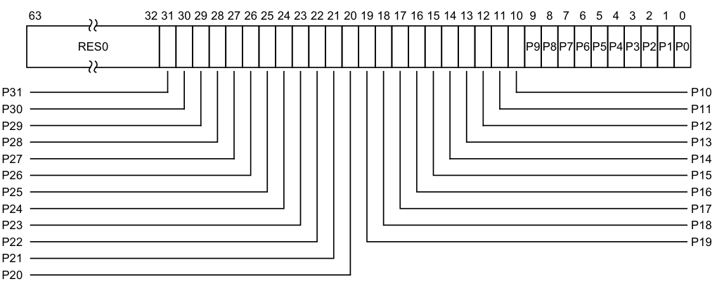
Image text
63 32 31 30 29 28 27 26 25 24 23 22 21 20 19 18 17 16 15 14 13 12 11 10 9 8 7 6 5 4 3 2 1 0
RES0 P9 P8 P7 P6 P5 P4 P3 P2 P1 P0
P31 P10
P30 P11
P29 P12
P28 P13
P27 P14
P26 P15
P25 P16
P24 P17
P23 P18
P22 P19
P21
P20
P, bit [x], for x = 31 to 0
Group 1 interrupt active priorities. Possible values of each bit are:
0b0 There is no Group 1 interrupt active with this priority level, or all active Group 1 interrupts with this priority level have undergone priority-drop.
0b1 There is a Group 1 interrupt active with this priority level which has not undergone priority drop.
The correspondence between priority levels and bits depends on the number of bits of priority that are implemented.
If 5 bits of preemption are implemented (bits [7:3] of priority), then there are 32 preemption levels, and the active state of these preemption levels are held in ICH_AP1R0_EL2 in the bits corresponding to Priority[7:3]. If 6 bits of preemption are implemented (bits [7:2] of priority), then there are 64 preemption levels, and:
-
The active state of preemption levels 0 - 124 are held in ICH_AP1R0_EL2 in the bits corresponding to 0:Priority[6:2].
-
The active state of preemption levels 128 - 252 are held in ICH_AP1R1_EL2 in the bits corresponding to 1:Priority[6:2].
If 7 bits of preemption are implemented (bits [7:1] of priority), then there are 128 preemption levels, and:
-
The active state of preemption levels 0 - 62 are held in ICH_AP1R0_EL2 in the bits corresponding to 00:Priority[5:1].
-
The active state of preemption levels 64 - 126 are held in ICH_AP1R1_EL2 in the bits corresponding to 01:Priority[5:1].
-
The active state of preemption levels 128 - 190 are held in ICH_AP1R2_EL2 in the bits corresponding to 10:Priority[5:1].
-
The active state of preemption levels 192 - 254 are held in ICH_AP1R3_EL2 in the bits corresponding to 11:Priority[5:1].
Note Having the bit corresponding to a priority set to 1 in both ICH_AP0R
_EL2 and
ICH_AP1R
On a Warm reset, this field resets to 0.
This register is always used for legacy VMs, regardless of the group of the virtual interrupt. Reads and writes to GICV_APR
Accessing the ICH_AP1R_EL2
ICH_AP1R1_EL2 is only implemented in implementations that support 6 or more bits of preemption. ICH_AP1R2_EL2 and ICH_AP1R3_EL2 are only implemented in implementations that support 7 bits of preemption. Unimplemented registers are UNDEFINED.
Note The number of bits of preemption is indicated by ICH_VTR_EL2.PREbits
Writing to these registers with any value other than the last read value of the register (or 0x00000000 for a newly set up virtual machine) can result in UNPREDICTABLE behavior of the virtual interrupt prioritization system allowing either:
Writing to the active priority registers in any order other than the following order will result in UNPREDICTABLE behavior:
Accesses to this register use the following encodings in the System instruction encoding space:
MRS , ICH_AP1R_EL2
| op0 | op1 | CRn | CRm | op2 |
|---|---|---|---|---|
| 0b11 | 0b100 | 0b1100 | 0b1001 | 0b0:n[1:0] |
if PSTATE.EL == EL0 then UNDEFINED;
elsif PSTATE.EL == EL1 then
if EL2Enabled() && HCR_EL2.<NV2,NV> == '11' then
return NVMem[0x4A0+8*UInt(op2<1:0>)];
elsif EL2Enabled() && HCR_EL2.NV == '1' then AArch64.SystemAccessTrap(EL2, 0x18);
else UNDEFINED;
elsif PSTATE.EL == EL2 then
if ICC_SRE_EL2.SRE == '0' then AArch64.SystemAccessTrap(EL2, 0x18);
else return ICH_AP1R_EL2[UInt(op2<1:0>)];
elsif PSTATE.EL == EL3 then
if ICC_SRE_EL3.SRE == '0' then AArch64.SystemAccessTrap(EL3, 0x18);
else return ICH_AP1R_EL2[UInt(op2<1:0>)];
MSR ICH_AP1R_EL2,
| op0 | op1 | CRn | CRm | op2 |
|---|---|---|---|---|
| 0b11 | 0b100 | 0b1100 | 0b1001 | 0b0:n[1:0] |
if PSTATE.EL == EL0 then UNDEFINED;
elsif PSTATE.EL == EL1 then
if EL2Enabled() && HCR_EL2.<NV2,NV> == '11' then NVMem[0x4A0+8*UInt(op2<1:0>)] = X[t];
elsif EL2Enabled() && HCR_EL2.NV == '1' then AArch64.SystemAccessTrap(EL2, 0x18);
else UNDEFINED;
elsif PSTATE.EL == EL2 then
if ICC_SRE_EL2.SRE == '0' then AArch64.SystemAccessTrap(EL2, 0x18);
else
ICH_AP1R_EL2[UInt(op2<1:0>)] = X[t];
elsif PSTATE.EL == EL3 then
if ICC_SRE_EL3.SRE == '0' then AArch64.SystemAccessTrap(EL3, 0x18);
else ICH_AP1R_EL2[UInt(op2<1:0>)] = X[t];
12.4.3 ICH_EISR_EL2, Interrupt Controller End of Interrupt Status Register
The ICH_EISR_EL2 characteristics are:
Purpose
Indicates which List registers have outstanding EOI maintenance interrupts.
Configurations
AArch64 System register ICH_EISR_EL2 bits [31:0] are architecturally mapped to AArch32 System register ICH_EISR[31:0].
If EL2 is not implemented, this register is RES0 from EL3.
This register has no effect if EL2 is not enabled in the current Security state.
Attributes
ICH_EISR_EL2 is a 64-bit register.
Field descriptions
The ICH_EISR_EL2 bit assignments are:
Image text
63 16 15 14 13 12 11 10 9 8 7 6 5 4 3 2 1 0
RES0
Status15 Status0
Status1
Status2
Status3
Status4
Status5
Status6
Status7
Status8
Status9
Status10
Status11
Status12
Status13
Status14
Status, bit [n], for n = 15 to 0
EOI maintenance interrupt status bit for List register
-
0b0 List register
, ICH_LR _EL2, does not have an EOI maintenance interrupt. -
0b1 List register
, ICH_LR _EL2, has an EOI maintenance interrupt that has not been handled.
For any ICH_LR
-
ICH_LR
_EL2.State is 0b00. -
ICH_LR
_EL2.HW is 0. -
ICH_LR
_EL2.EOI (bit [41]) is 1, indicating that when the interrupt corresponding to that List register is deactivated, a maintenance interrupt is asserted. Otherwise the status bit takes the value 0.
Accessing the ICH_EISR_EL2
Accesses to this register use the following encodings in the System instruction encoding space:
MRS , ICH_EISR_EL2
| op0 | op1 | CRn | CRm | op2 |
|---|---|---|---|---|
| 0b11 | 0b100 | 0b1100 | 0b1011 | 0b011 |
if PSTATE.EL == EL0 then UNDEFINED;
elsif PSTATE.EL == EL1 then
if EL2Enabled() && HCR_EL2.NV == '1' then AArch64.SystemAccessTrap(EL2, 0x18);
else UNDEFINED;
elsif PSTATE.EL == EL2 then
if ICC_SRE_EL2.SRE == '0' then AArch64.SystemAccessTrap(EL2, 0x18);
else return ICH_EISR_EL2;
elsif PSTATE.EL == EL3 then
if ICC_SRE_EL3.SRE == '0' then AArch64.SystemAccessTrap(EL3, 0x18);
else return ICH_EISR_EL2;
12.4.4 ICH_ELRSR_EL2, Interrupt Controller Empty List Register Status Register
The ICH_ELRSR_EL2 characteristics are:
Purpose
These registers can be used to locate a usable List register when the hypervisor is delivering an interrupt to a VM.
Configurations
AArch64 System register ICH_ELRSR_EL2 bits [31:0] are architecturally mapped to AArch32 System register ICH_ELRSR[31:0].
If EL2 is not implemented, this register is RES0 from EL3.
This register has no effect if EL2 is not enabled in the current Security state.
Attributes
ICH_ELRSR_EL2 is a 64-bit register.
Field descriptions
The ICH_ELRSR_EL2 bit assignments are:
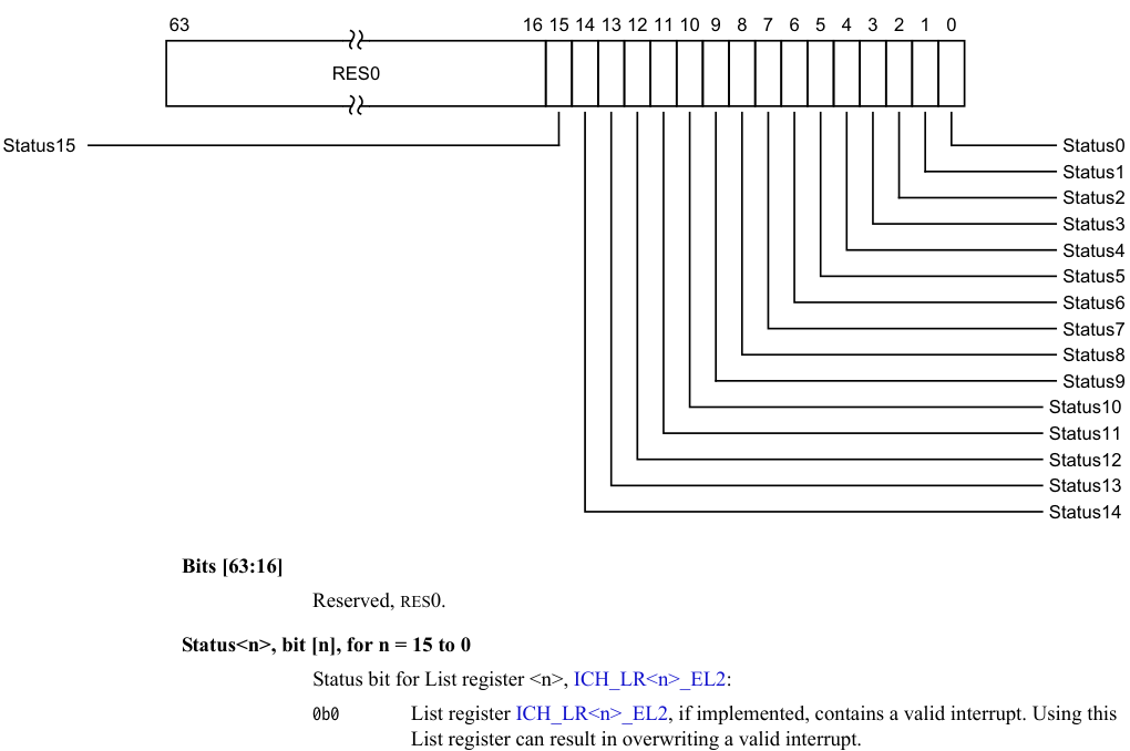
Image text
63 16 15 14 13 12 11 10 9 8 7 6 5 4 3 2 1 0
RES0
Status15 Status0
Status1
Status2
Status3
Status4
Status5
Status6
Status7
Status8
Status9
Status10
Status11
Status12
Status13
Status14
Bits [63:16]
Reserved, RES0.
Status
Status bit for List register
0b0 List register ICH_LR
List register can result in overwriting a valid interrupt.
For any List register
Accessing the ICH_ELRSR_EL2
Accesses to this register use the following encodings in the System instruction encoding space:
MRS , ICH_ELRSR_EL2
| op0 | op1 | CRn | CRm | op2 |
|---|---|---|---|---|
| 0b11 | 0b100 | 0b1100 | 0b1011 | 0b101 |
if PSTATE.EL == EL0 then UNDEFINED;
elsif PSTATE.EL == EL1 then
if EL2Enabled() && HCR_EL2.NV == '1' then AArch64.SystemAccessTrap(EL2, 0x18);
else UNDEFINED;
elsif PSTATE.EL == EL2 then
if ICC_SRE_EL2.SRE == '0' then AArch64.SystemAccessTrap(EL2, 0x18);
else return ICH_ELRSR_EL2;
elsif PSTATE.EL == EL3 then
if ICC_SRE_EL3.SRE == '0' then AArch64.SystemAccessTrap(EL3, 0x18);
else return ICH_ELRSR_EL2;
12.4.5 ICH_HCR_EL2, Interrupt Controller Hyp Control Register
The ICH_HCR_EL2 characteristics are:
Purpose
Controls the environment for VMs.
Configurations
AArch64 System register ICH_HCR_EL2 bits [31:0] are architecturally mapped to AArch32 System register ICH_HCR[31:0].
If EL2 is not implemented, this register is RES0 from EL3.
This register has no effect if EL2 is not enabled in the current Security state.
Attributes
ICH_HCR_EL2 is a 64-bit register.
Field descriptions
The ICH_HCR_EL2 bit assignments are:
Image text
63 32 31 27 26 16 15 14 13 12 11 10 9 8 7 6 5 4 3 2 1 0
RES0 EOIcount RES0 TC En
DVIM UIE
LRENPIE
NPIE
VGrp0EIE
VGrp0DIE
VGrp1EIE
VGrp1DIE
vSGIEOICount
RES0
TALL0
TALL1
TSEI
TDIR
EOIcount, bits [31:27]
This field is incremented whenever a successful write to a virtual EOIR or DIR register would have resulted in a virtual interrupt deactivation. That is either:
-
A virtual write to EOIR with a valid interrupt identifier that is not in the LPI range (that is < 8192) when EOI mode is zero and no List Register was found.
-
A virtual write to DIR with a valid interrupt identifier that is not in the LPI range (that is < 8192) when EOI mode is one and no List Register was found.
This allows software to manage more active interrupts than there are implemented List Registers.
It is CONSTRAINED UNPREDICTABLE whether a virtual write to EOIR that does not clear a bit in the Active Priorities registers (ICH_AP0R
- Increment EOIcount. • Leave EOIcount unchanged. On a Warm reset, this field resets to 0.
Bits [26:16]
Reserved, RES0.
DVIM, bit [15]
When ICH_VTR_EL2.DVIM == 1:
DVIM
Directly-injected Virtual Interrupt Mask.
0b0 This control has no effect on the signalling of virtual interrupts.
0b1 Virtual interrupts received via direct-injection are not presented to the virtual CPU interface and not considered when determining the highest priority pending virtual interrupt.
On a Warm reset, this field resets to 0.
Otherwise:
Reserved, RES0.
When ICH_VTR_EL2.DVIM == 1:
DVIM
Directly-injected Virtual Interrupt Mask.
0b0 This control has no effect on the signalling of virtual interrupts. 0b1 Virtual interrupts received via direct-injection are not presented to the virtual CPU interface and not considered when determining the highest priority pending virtual interrupt.
On a Warm reset, this field resets to 0.
Otherwise:
Reserved, RES0.
TDIR, bit [14]
Trap EL1 writes to ICC_DIR_EL1 and ICV_DIR_EL1.
0b0 EL1 writes of ICC_DIR_EL1 and ICV_DIR_EL1 are not trapped to EL2, unless trapped by other mechanisms.
0b1 EL1 writes of ICV_DIR_EL1 are trapped to EL2. It is IMPLEMENTATION DEFINED whether writes of ICC_DIR_EL1 are trapped. Not trapping ICC_DIR_EL1 writes is DEPRECATED.
Support for this bit is OPTIONAL, with support indicated by ICH_VTR_EL2.
If the implementation does not support this trap, this bit is RES0.
Arm deprecates not including this trap bit.
On a Warm reset, this field resets to 0.
TSEI, bit [13]
Trap all locally generated SEIs. This bit allows the hypervisor to intercept locally generated SEIs that would otherwise be taken at EL1.
0b0 Locally generated SEIs do not cause a trap to EL2. 0b1 Locally generated SEIs trap to EL2.
If ICH_VTR_EL2.SEIS is 0, this bit is RES0. On a Warm reset, this field resets to 0.
TALL1, bit [12]
Trap all EL1 accesses to ICC_* and ICV_* System registers for Group 1 interrupts to EL2. 0b0 EL1 accesses to ICC_* and ICV_* registers for Group 1 interrupts proceed as normal. 0b1 EL1 accesses to ICC_* and ICV_* registers for Group 1 interrupts trap to EL2. On a Warm reset, this field resets to 0.
TALL0, bit [11]
Trap all EL1 accesses to ICC_* and ICV_* System registers for Group 0 interrupts to EL2. 0b0 EL1 accesses to ICC_* and ICV_* registers for Group 0 interrupts proceed as normal. 0b1 EL1 accesses to ICC_* and ICV_* registers for Group 0 interrupts trap to EL2. On a Warm reset, this field resets to 0.
TC, bit [10]
Trap all EL1 accesses to System registers that are common to Group 0 and Group 1 to EL2. 0b0 EL1 accesses to common registers proceed as normal. 0b1 EL1 accesses to common registers trap to EL2. This affects accesses to ICC_SGI0R_EL1, ICC_SGI1R_EL1, ICC_ASGI1R_EL1, ICC_CTLR_EL1, ICC_DIR_EL1, ICC_PMR_EL1, ICC_RPR_EL1, ICV_CTLR_EL1, ICV_DIR_EL1, ICV_PMR_EL1, and ICV_RPR_EL1.
On a Warm reset, this field resets to 0.
Bit [9]
Reserved, RES0.
vSGIEOICount, bit [8]
When FEAT_GICv4p1 is implemented:
vSGIEOICount
Controls whether deactivation of virtual SGIs can increment ICH_HCR_EL2.EOIcount 0b0 Deactivation of virtual SGIs can increment ICH_HCR_EL2.EOIcount. 0b1 Deactivation of virtual SGIs does not increment ICH_HCR_EL2.EOIcount. On a Warm reset, this field resets to 0.
Otherwise:
Reserved, RES0.
VGrp1DIE, bit [7]
VM Group 1 Disabled Interrupt Enable. Enables the signaling of a maintenance interrupt while signaling of Group 1 interrupts from the virtual CPU interface to the connected vPE is disabled: 0b0 Maintenance interrupt disabled. 0b1 Maintenance interrupt signaled when ICH_VMCR_EL2.VENG1 is 0. On a Warm reset, this field resets to 0.
VGrp1EIE, bit [6]
VM Group 1 Enabled Interrupt Enable. Enables the signaling of a maintenance interrupt while signaling of Group 1 interrupts from the virtual CPU interface to the connected vPE is enabled: 0b0 Maintenance interrupt disabled. 0b1 Maintenance interrupt signaled when ICH_VMCR_EL2.VENG1 is 1. On a Warm reset, this field resets to 0.
VGrp0DIE, bit [5]
VM Group 0 Disabled Interrupt Enable. Enables the signaling of a maintenance interrupt while signaling of Group 0 interrupts from the virtual CPU interface to the connected vPE is disabled: 0b0 Maintenance interrupt disabled. 0b1 Maintenance interrupt signaled when ICH_VMCR_EL2.VENG0 is 0. On a Warm reset, this field resets to 0.
VGrp0EIE, bit [4]
VM Group 0 Enabled Interrupt Enable. Enables the signaling of a maintenance interrupt while signaling of Group 0 interrupts from the virtual CPU interface to the connected vPE is enabled: 0b0 Maintenance interrupt disabled. 0b1 Maintenance interrupt signaled when ICH_VMCR_EL2.VENG0 is 1. On a Warm reset, this field resets to 0.
NPIE, bit [3]
No Pending Interrupt Enable. Enables the signaling of a maintenance interrupt when there are no List registers with the State field set to 0b01 (pending): 0b0 Maintenance interrupt disabled. 0b1 Maintenance interrupt signaled while the List registers contain no interrupts in the pending state.
On a Warm reset, this field resets to 0.
LRENPIE, bit [2]
List Register Entry Not Present Interrupt Enable. Enables the signaling of a maintenance interrupt while the virtual CPU interface does not have a corresponding valid List register entry for an EOI request: 0b0 Maintenance interrupt disabled. 0b1 Maintenance interrupt is asserted while the EOIcount field is not 0. On a Warm reset, this field resets to 0.
UIE, bit [1]
Underflow Interrupt Enable. Enables the signaling of a maintenance interrupt when the List registers are empty, or hold only one valid entry:
0b0 Maintenance interrupt disabled. 0b1 Maintenance interrupt is asserted if none, or only one, of the List register entries is marked as a valid interrupt.
On a Warm reset, this field resets to 0.
En, bit [0]
Enable. Global enable bit for the virtual CPU interface:
0b0 Virtual CPU interface operation disabled.
0b1 Virtual CPU interface operation enabled.
When this field is set to 0:
-
The virtual CPU interface does not signal any maintenance interrupts.
-
The virtual CPU interface does not signal any virtual interrupts.
-
A read of ICV_IAR0_EL1, ICV_IAR1_EL1, GICV_IAR or GICV_AIAR returns a spurious interrupt ID.
Note This field is RES0 when SCR_EL3.{NS,EEL2}=={0,0}
On a Warm reset, this field resets to 0.
Accessing the ICH_HCR_EL2
Accesses to this register use the following encodings in the System instruction encoding space:
MRS , ICH_HCR_EL2
| op0 | op1 | CRn | CRm | op2 |
|---|---|---|---|---|
| 0b11 | 0b100 | 0b1100 | 0b1011 | 0b000 |
if PSTATE.EL == EL0 then UNDEFINED;
elsif PSTATE.EL == EL1 then
if EL2Enabled() && HCR_EL2.<NV2,NV> == '11' then
return NVMem[0x4C0];
elsif EL2Enabled() && HCR_EL2.NV == '1' then AArch64.SystemAccessTrap(EL2, 0x18);
else UNDEFINED;
elsif PSTATE.EL == EL2 then
if ICC_SRE_EL2.SRE == '0' then AArch64.SystemAccessTrap(EL2, 0x18);
else return ICH_HCR_EL2;
elsif PSTATE.EL == EL3 then
if ICC_SRE_EL3.SRE == '0' then AArch64.SystemAccessTrap(EL3, 0x18);
else return ICH_HCR_EL2;
MSR ICH_HCR_EL2,
| op0 | op1 | CRn | CRm | op2 |
|---|---|---|---|---|
| 0b11 | 0b100 | 0b1100 | 0b1011 | 0b000 |
if PSTATE.EL == EL0
then
UNDEFINED;
elsif PSTATE.EL == EL1
then if EL2Enabled() && HCR_EL2.<NV2,NV> == '11'
then NVMem[0x4C0] = X[t];
elsif EL2Enabled() && HCR_EL2.NV == '1' then
AArch64.SystemAccessTrap(EL2, 0x18);
else UNDEFINED;
elsif PSTATE.EL == EL2
then if ICC_SRE_EL2.SRE == '0'
then AArch64.SystemAccessTrap(EL2, 0x18);
else ICH_HCR_EL2 = X[t];
elsif PSTATE.EL == EL3
then if ICC_SRE_EL3.SRE == '0'
then AArch64.SystemAccessTrap(EL3, 0x18);
else ICH_HCR_EL2 = X[t];
12.4.6 ICH_LR_EL2, Interrupt Controller List Registers, n = 0 - 15
The ICH_LR
Purpose
Provides interrupt context information for the virtual CPU interface.
Configurations
AArch64 System register ICH_LR
AArch64 System register ICH_LR
If EL2 is not implemented, this register is RES0 from EL3.
If list register n is not implemented, then accesses to this register are UNDEFINED.
This register has no effect if EL2 is not enabled in the current Security state.
Attributes
ICH_LR
Field descriptions
The ICH_LR
| HW Group | | State 63 62 61 60 RES0 59 56 Priority 55 48 RES0 47 45 pINTID 44 32 vINTID 31 0 | State 63 62 61 60 RES0 59 56 Priority 55 48 RES0 47 45 pINTID 44 32 vINTID 31 0 | State 63 62 61 60 RES0 59 56 Priority 55 48 RES0 47 45 pINTID 44 32 vINTID 31 0 | State 63 62 61 60 RES0 59 56 Priority 55 48 RES0 47 45 pINTID 44 32 vINTID 31 0 | State 63 62 61 60 RES0 59 56 Priority 55 48 RES0 47 45 pINTID 44 32 vINTID 31 0 | State 63 62 61 60 RES0 59 56 Priority 55 48 RES0 47 45 pINTID 44 32 vINTID 31 0 | State 63 62 61 60 RES0 59 56 Priority 55 48 RES0 47 45 pINTID 44 32 vINTID 31 0 | State 63 62 61 60 RES0 59 56 Priority 55 48 RES0 47 45 pINTID 44 32 vINTID 31 0 | State 63 62 61 60 RES0 59 56 Priority 55 48 RES0 47 45 pINTID 44 32 vINTID 31 0 | State 63 62 61 60 RES0 59 56 Priority 55 48 RES0 47 45 pINTID 44 32 vINTID 31 0 | |—|—|— State RES0 Priority RES0 pINTID vINTID |— State |—|—|—|— RES0 |— Priority |— RES0 |— pINTID |— vINTID | ||||||||||||| |||||||||||||
State, bits [63:62]
The state of the interrupt: 0b00 Invalid (Inactive). 0b01 Pending. 0b10 Active. 0b11 Pending and active.
The GIC updates these state bits as virtual interrupts proceed through the interrupt life cycle. Entries in the invalid state are ignored, except for the purpose of generating virtual maintenance interrupts. For hardware interrupts, the pending and active state is held in the physical Distributor rather than the virtual CPU interface. A hypervisor must only use the pending and active state for software originated interrupts, which are typically associated with virtual devices, or SGIs.
On a Warm reset, this field resets to an architecturally UNKNOWN value.
HW, bit [61]
Indicates whether this virtual interrupt maps directly to a hardware interrupt, meaning that it corresponds to a physical interrupt. Deactivation of the virtual interrupt also causes the deactivation of the physical interrupt with the ID that the pINTID field indicates.
0b0 The interrupt is triggered entirely by software. No notification is sent to the Distributor when the virtual interrupt is deactivated.
0b1 The interrupt maps directly to a hardware interrupt. A deactivate interrupt request is sent to the Distributor when the virtual interrupt is deactivated, using the pINTID field from this register to indicate the physical interrupt ID. If ICH_VMCR_EL2.VEOIM is 0, this request corresponds to a write to ICC_EOIR0_EL1 or ICC_EOIR1_EL1. Otherwise, it corresponds to a write to ICC_DIR_EL1.
On a Warm reset, this field resets to an architecturally UNKNOWN value.
Group, bit [60]
Indicates the group for this virtual interrupt.
0b0 This is a Group 0 virtual interrupt. ICH_VMCR_EL2.VFIQEn determines whether it is signaled as a virtual IRQ or as a virtual FIQ, and ICH_VMCR_EL2.VENG0 enables signaling of this interrupt to the virtual machine.
0b1 This is a Group 1 virtual interrupt, signaled as a virtual IRQ. ICH_VMCR_EL2.VENG1 enables the signalling of this interrupt to the virtual machine.
If ICH_VMCR_EL2.VCBPR is 0, then ICC_BPR1_EL1 determines if a pending Group 1 interrupt has sufficient priority to preempt current execution. Otherwise, ICH_LR
On a Warm reset, this field resets to an architecturally UNKNOWN value.
Bits [59:56]
Reserved, RES0.
Priority, bits [55:48]
The priority of this interrupt.
It is IMPLEMENTATION DEFINED how many bits of priority are implemented, though at least five bits must be implemented. Unimplemented bits are RES0 and start from bit[48] up to bit[50]. The number of implemented bits can be discovered from ICH_VTR_EL2.PRIbits.
On a Warm reset, this field resets to an architecturally UNKNOWN value.
Bits [47:45]
Reserved, RES0.
pINTID, bits [44:32]
Physical INTID, for hardware interrupts.
When ICH_LR
-
Bits[44:42] : RES0.
-
Bit[41] : EOI. If this bit is 1, then when the interrupt identified by vINTID is deactivated, a maintenance interrupt is asserted.
-
Bits[40:32] : RES0.
When ICH_LR
-
This field indicates the physical INTID. This field is only required to implement enough bits to hold a valid value for the implemented INTID size. Any unused higher order bits are RES0.
-
When ICC_CTLR_EL1.ExtRange is 0, then bits[44:42] of this field are RES0.
-
If the value of pINTID is not a vald INTID, behavior is UNPREDICTABLE. If the value of pINTID indicates a PPI, this field applies to the PPI associated with this same physical PE ID as the virtual CPU interface requesting the deactivation.
A hardware physical identifier is only required in List Registers for interrupts that require deactivation. This means only 13 bits of Physical INTID are required, regardless of the number specified by ICC_CTLR_EL1.IDbits.
On a Warm reset, this field resets to an architecturally UNKNOWN value.
vINTID, bits [31:0]
Virtual INTID of the interrupt.
If the value of vINTID is 1020-1023 and ICH_LR
Behavior is UNPREDICTABLE if two or more List Registers specify the same vINTID when:
-
ICH_LR
_EL2.State == 0b01. -
ICH_LR
_EL2.State == 0b10. -
ICH_LR
_EL2.State == 0b11.
It is IMPLEMENTATION DEFINED how many bits are implemented, though at least 16 bits must be implemented. Unimplemented bits are RES0. The number of implemented bits can be discovered from ICH_VTR_EL2.IDbits.
When ICC_SRE_EL1.SRE == 0, specifying a vINTID in the LPI range is UNPREDICTABLE Note When a VM is using memory-mapped access to the GIC, software must ensure that the correct source PE ID is provided in bits[12:10].
On a Warm reset, this field resets to an architecturally UNKNOWN value.
Accessing the ICH_LR_EL2
Accesses to this register use the following encodings in the System instruction encoding space:
MRS , ICH_LR_EL2
| op0 | op1 | CRn | CRm | op2 |
|---|---|---|---|---|
| 0b11 | 0b100 | 0b1100 | 0b110:n[3] | n[2:0] |
if PSTATE.EL == EL0 then UNDEFINED;
elsif PSTATE.EL == EL1 then
if EL2Enabled() && HCR_EL2.<NV2,NV> == '11' then
return NVMem[0x400+8*UInt(CRm<0>:op2<2:0>)];
elsif EL2Enabled() && HCR_EL2.NV == '1' then AArch64.SystemAccessTrap(EL2, 0x18);
else UNDEFINED;
elsif PSTATE.EL == EL2 then
if ICC_SRE_EL2.SRE == '0' then AArch64.SystemAccessTrap(EL2, 0x18);
else return ICH_LR_EL2[UInt(CRm<0>:op2<2:0>)];
elsif PSTATE.EL == EL3 then
if ICC_SRE_EL3.SRE == '0' then AArch64.SystemAccessTrap(EL3, 0x18);
else return ICH_LR_EL2[UInt(CRm<0>:op2<2:0>)];
MSR ICH_LR_EL2,
| op0 | op1 | CRn | CRm | op2 |
|---|---|---|---|---|
| 0b11 | 0b100 | 0b1100 | 0b110:n[3] | n[2:0] |
if PSTATE.EL == EL0 then UNDEFINED;
elsif PSTATE.EL == EL1 then
if EL2Enabled() && HCR_EL2.<NV2,NV> == '11' then
NVMem[0x400+8*UInt(CRm<0>:op2<2:0>)] = X[t];
elsif EL2Enabled() && HCR_EL2.NV == '1' then AArch64.SystemAccessTrap(EL2, 0x18);
else UNDEFINED;
elsif PSTATE.EL == EL2 then
if ICC_SRE_EL2.SRE == '0' then AArch64.SystemAccessTrap(EL2, 0x18);
else ICH_LR_EL2[UInt(CRm<0>:op2<2:0>)] = X[t];
elsif PSTATE.EL == EL3 then
if ICC_SRE_EL3.SRE == '0' then AArch64.SystemAccessTrap(EL3, 0x18);
else ICH_LR_EL2[UInt(CRm<0>:op2<2:0>)] = X[t];
12.4.7 ICH_MISR_EL2, Interrupt Controller Maintenance Interrupt State Register
The ICH_MISR_EL2 characteristics are:
Purpose
Indicates which maintenance interrupts are asserted.
Configurations
AArch64 System register ICH_MISR_EL2 bits [31:0] are architecturally mapped to AArch32 System register ICH_MISR[31:0].
If EL2 is not implemented, this register is RES0 from EL3.
This register has no effect if EL2 is not enabled in the current Security state.
Attributes
ICH_MISR_EL2 is a 64-bit register.
Field descriptions
The ICH_MISR_EL2 bit assignments are:
Image text
63 8 7 6 5 4 3 2 1 0
RES0 NP U
EOI
LRENP
VGrp0E
VGrp0D
VGrp1E
VGrp1D
VGrp1D, bit [7]
vPE Group 1 Disabled.
0b0 vPE Group 1 Disabled maintenance interrupt not asserted.
0b1 vPE Group 1 Disabled maintenance interrupt asserted.
This maintenance interrupt is asserted when ICH_HCR_EL2.VGrp1DIE==1 and ICH_VMCR_EL2.VENG1==is 0.
On a Warm reset, this field resets to 0.
VGrp1E, bit [6]
vPE Group 1 Enabled.
0b0 vPE Group 1 Enabled maintenance interrupt not asserted. 0b1 vPE Group 1 Enabled maintenance interrupt asserted. This maintenance interrupt is asserted when ICH_HCR_EL2.VGrp1EIE==1 and ICH_VMCR_EL2.VENG1==is 1.
On a Warm reset, this field resets to 0.
VGrp0D, bit [5]
vPE Group 0 Disabled. 0b0 vPE Group 0 Disabled maintenance interrupt not asserted. 0b1 vPE Group 0 Disabled maintenance interrupt asserted. This maintenance interrupt is asserted when ICH_HCR_EL2.VGrp0DIE==1 and ICH_VMCR_EL2.VENG0==0. On a Warm reset, this field resets to 0.
VGrp0E, bit [4]
vPE Group 0 Enabled. 0b0 vPE Group 0 Enabled maintenance interrupt not asserted. 0b1 vPE Group 0 Enabled maintenance interrupt asserted. This maintenance interrupt is asserted when ICH_HCR_EL2.VGrp0EIE==1 and ICH_VMCR_EL2.VENG0==1. On a Warm reset, this field resets to 0. NP, bit [3] No Pending. 0b0 No Pending maintenance interrupt not asserted. 0b1 No Pending maintenance interrupt asserted. This maintenance interrupt is asserted when ICH_HCR_EL2.NPIE==1 and no List register is in pending state.
On a Warm reset, this field resets to 0.
LRENP, bit [2]
List Register Entry Not Present. 0b0 List Register Entry Not Present maintenance interrupt not asserted. 0b1 List Register Entry Not Present maintenance interrupt asserted. This maintenance interrupt is asserted when ICH_HCR_EL2.LRENPIE==1 and ICH_HCR_EL2.EOIcount is non-zero. On a Warm reset, this field resets to 0. U, bit [1] Underflow. 0b0 Underflow maintenance interrupt not asserted. 0b1 Underflow maintenance interrupt asserted. This maintenance interrupt is asserted when ICH_HCR_EL2.UIE==1 and zero or one of the List register entries are marked as a valid interrupt, that is, if the corresponding ICH_LR
Accessing the ICH_MISR_EL2
Accesses to this register use the following encodings in the System instruction encoding space:
MRS , ICH_MISR_EL2
| op0 | op1 | CRn | CRm | op2 |
|---|---|---|---|---|
| 0b11 | 0b100 | 0b1100 | 0b1011 | 0b010 |
if PSTATE.EL == EL0 then UNDEFINED;
elsif PSTATE.EL == EL1 then
if EL2Enabled() && HCR_EL2.NV == '1' then AArch64.SystemAccessTrap(EL2, 0x18);
else UNDEFINED;
elsif PSTATE.EL == EL2 then
if ICC_SRE_EL2.SRE == '0' then AArch64.SystemAccessTrap(EL2, 0x18);
else return ICH_MISR_EL2;
elsif PSTATE.EL == EL3 then
if ICC_SRE_EL3.SRE == '0' then AArch64.SystemAccessTrap(EL3, 0x18);
else return ICH_MISR_EL2;
12.4.8 ICH_VMCR_EL2, Interrupt Controller Virtual Machine Control Register
The ICH_VMCR_EL2 characteristics are:
Purpose
Enables the hypervisor to save and restore the virtual machine view of the GIC state.
Configurations
AArch64 System register ICH_VMCR_EL2 bits [31:0] are architecturally mapped to AArch32 System register ICH_VMCR[31:0].
If EL2 is not implemented, this register is RES0 from EL3.
This register has no effect if EL2 is not enabled in the current Security state.
Attributes
ICH_VMCR_EL2 is a 64-bit register.
Field descriptions
The ICH_VMCR_EL2 bit assignments are:
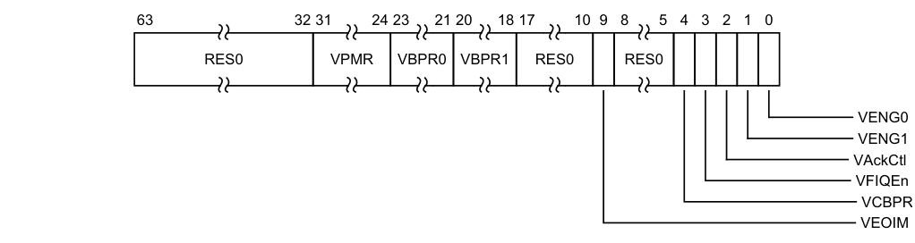
Image text
63 32 31 24 23 21 20 18 17 10 9 8 5 4 3 2 1 0
RES0 VPMR VBPR0 VBPR1 RES0 RES0
VENG0
VENG1
VAckCtl
VFIQEn
VCBPR
VEOIM
VPMR, bits [31:24]
Virtual Priority Mask. The priority mask level for the virtual CPU interface. If the priority of a pending virtual interrupt is higher than the value indicated by this field, the interface signals the virtual interrupt to the PE.
This field is an alias of ICV_PMR_EL1.Priority.
VBPR0, bits [23:21]
Virtual Binary Point Register, Group 0. Defines the point at which the priority value fields split into two parts, the group priority field and the subpriority field. The group priority field determines Group 0 interrupt preemption, and also determines Group 1 interrupt preemption if ICH_VMCR_EL2.VCBPR == 1.
This field is an alias of ICV_BPR0_EL1.BinaryPoint.
The minimum value of this field is determined by ICH_VTR_EL2.PREbits. An attempt to program the binary point field to a value less than the minimum value sets the field to the minimum value.
VBPR1, bits [20:18]
Virtual Binary Point Register, Group 1. Defines the point at which the priority value fields split into two parts, the group priority field and the subpriority field. The group priority field determines Group 1 interrupt preemption if ICH_VMCR_EL2.VCBPR == 0.
This field is an alias of ICV_BPR1_EL1.BinaryPoint. This field is always accessible to EL2 accesses, regardless of the setting of the ICH_VMCR_EL2.VCBPR field.
For Non-secure writes, the minimum value of this field is the minimum value of ICH_VMCR_EL2.VBPR0 plus one.
For Secure writes, the minimum value of this field is the minimum value of ICH_VMCR_EL2.VBPR0.
An attempt to program the binary point field to a value less than the minimum value sets the field to the minimum value.
Bits [17:10]
Reserved, RES0.
VEOIM, bit [9]
Virtual EOI mode. Controls whether a write to an End of Interrupt register also deactivates the virtual interrupt: 0b0 ICV_EOIR0_EL1 and ICV_EOIR1_EL1 provide both priority drop and interrupt deactivation functionality. Accesses to ICV_DIR_EL1 are UNPREDICTABLE. 0b1 ICV_EOIR0_EL1 and ICV_EOIR1_EL1 provide priority drop functionality only. ICV_DIR_EL1 provides interrupt deactivation functionality. This bit is an alias of ICV_CTLR_EL1.EOImode.
Bits [8:5]
Reserved, RES0.
VCBPR, bit [4]
Virtual Common Binary Point Register. Possible values of this bit are:
0b0 ICV_BPR1_EL1 determines the preemption group for virtual Group 1 interrupts. 0b1 Reads of ICV_BPR1_EL1 return ICV_BPR0_EL1 plus one, saturated to 0b111. Writes to ICV_BPR1_EL1 are ignored.
This field is an alias of ICV_CTLR_EL1.CBPR.
VFIQEn, bit [3]
Virtual FIQ enable. Possible values of this bit are: 0b0 Group 0 virtual interrupts are presented as virtual IRQs. 0b1 Group 0 virtual interrupts are presented as virtual FIQs. This bit is an alias of GICV_CTLR.FIQEn.
In implementations where the Non-secure copy of ICC_SRE_EL1.SRE is always 1, this bit is RES1.
VAckCtl, bit [2]
Virtual AckCtl. Possible values of this bit are:
0b0 If the highest priority pending interrupt is Group 1, a read of GICV_IAR or GICV_HPPIR returns an INTID of 1022. 0b1 If the highest priority pending interrupt is Group 1, a read of GICV_IAR or GICV_HPPIR returns the INTID of the corresponding interrupt. This bit is an alias of GICV_CTLR.AckCtl. This field is supported for backwards compatibility with GICv2. Arm deprecates the use of this field.
In implementations where the Non-secure copy of ICC_SRE_EL1.SRE is always 1, this bit is RES0.
VENG1, bit [1]
Virtual Group 1 interrupt enable. Possible values of this bit are: 0b0 Virtual Group 1 interrupts are disabled. 0b1 Virtual Group 1 interrupts are enabled.
This bit is an alias of ICV_IGRPEN1_EL1.Enable.
VENG0, bit [0]
Virtual Group 0 interrupt enable. Possible values of this bit are:
0b0 Virtual Group 0 interrupts are disabled. 0b1 Virtual Group 0 interrupts are enabled. This bit is an alias of ICV_IGRPEN0_EL1.Enable.
Accessing the ICH_VMCR_EL2
When EL2 is using System register access, EL1 using either System register or memory-mapped access must be supported.
Accesses to this register use the following encodings in the System instruction encoding space:
MRS , ICH_VMCR_EL2
| op0 | op1 | CRn | CRm | op2 |
|---|---|---|---|---|
| 0b11 | 0b100 | 0b1100 | 0b1011 | 0b111 |
if PSTATE.EL == EL0 then UNDEFINED;
elsif PSTATE.EL == EL1 then
if EL2Enabled() && HCR_EL2.<NV2,NV> == '11' then
return NVMem[0x4C8];
elsif EL2Enabled() && HCR_EL2.NV == '1' then AArch64.SystemAccessTrap(EL2, 0x18);
else UNDEFINED;
elsif PSTATE.EL == EL2 then
if ICC_SRE_EL2.SRE == '0' then AArch64.SystemAccessTrap(EL2, 0x18);
else return ICH_VMCR_EL2;
elsif PSTATE.EL == EL3 then
if ICC_SRE_EL3.SRE == '0' then AArch64.SystemAccessTrap(EL3, 0x18);
else return ICH_VMCR_EL2;
MSR ICH_VMCR_EL2,
| op0 | op1 | CRn | CRm | op2 |
|---|---|---|---|---|
| 0b11 | 0b100 | 0b1100 | 0b1011 | 0b111 |
if PSTATE.EL == EL0 then UNDEFINED;
elsif PSTATE.EL == EL1 then
if EL2Enabled() && HCR_EL2.<NV2,NV> == '11' then NVMem[0x4C8] = X[t];
elsif EL2Enabled() && HCR_EL2.NV == '1' then AArch64.SystemAccessTrap(EL2, 0x18);
else UNDEFINED;
elsif PSTATE.EL == EL2 then
if ICC_SRE_EL2.SRE == '0' then
AArch64.SystemAccessTrap(EL2, 0x18);
else ICH_VMCR_EL2 = X[t];
elsif PSTATE.EL == EL3
then if ICC_SRE_EL3.SRE == '0'
then AArch64.SystemAccessTrap(EL3, 0x18);
else ICH_VMCR_EL2 = X[t];
12.4.9 ICH_VTR_EL2, Interrupt Controller VGIC Type Register
The ICH_VTR_EL2 characteristics are:
Purpose
Reports supported GIC virtualization features.
Configurations
AArch64 System register ICH_VTR_EL2 bits [31:0] are architecturally mapped to AArch32 System register ICH_VTR[31:0].
If EL2 is not implemented, all bits in this register are RES0 from EL3, except for nV4, which is RES1 from EL3.
This register has no effect if EL2 is not enabled in the current Security state.
Attributes
ICH_VTR_EL2 is a 64-bit register.
Field descriptions
The ICH_VTR_EL2 bit assignments are:
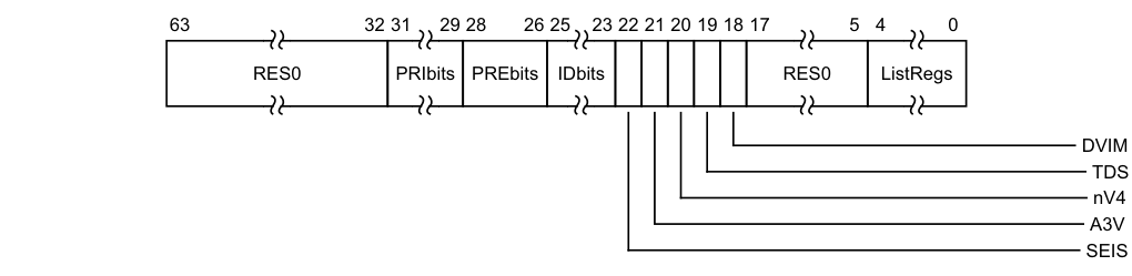
Image text
63 32 31 29 28 26 25 23 22 21 20 19 18 17 5 4 0
RES0 PRIbits PREbits IDbits RES0 ListRegs
DVIM
TDS
nV4
A3V
SEIS
PRIbits, bits [31:29]
Priority bits. The number of virtual priority bits implemented, minus one.
An implementation must implement at least 32 levels of virtual priority (5 priority bits). This field is an alias of ICV_CTLR_EL1.PRIbits.
PREbits, bits [28:26]
The number of virtual preemption bits implemented, minus one.
An implementation must implement at least 32 levels of virtual preemption priority (5 preemption bits).
The value of this field must be less than or equal to the value of ICH_VTR_EL2.PRIbits.
The maximum value of this field is 6, indicating 7 bits of preemption.
This field determines the minimum value of ICH_VMCR_EL2.VBPR0.
IDbits, bits [25:23]
The number of virtual interrupt identifier bits supported:
0b000 16 bits. 0b001 24 bits. All other values are reserved. This field is an alias of ICV_CTLR_EL1.IDbits.
SEIS, bit [22]
SEI Support. Indicates whether the virtual CPU interface supports generation of SEIs: 0b0 The virtual CPU interface logic does not support generation of SEIs. 0b1 The virtual CPU interface logic supports generation of SEIs. This bit is an alias of ICV_CTLR_EL1.SEIS.
A3V, bit [21]
Affinity 3 Valid. Possible values are: 0b0 The virtual CPU interface logic only supports zero values of Affinity 3 in SGI generation System registers. 0b1 The virtual CPU interface logic supports non-zero values of Affinity 3 in SGI generation System registers. This bit is an alias of ICV_CTLR_EL1.A3V.
nV4, bit [20]
Direct injection of virtual interrupts not supported. Possible values are: 0b0 The CPU interface logic supports direct injection of virtual interrupts. 0b1 The CPU interface logic does not support direct injection of virtual interrupts. In GICv3, the only permitted value is 0b1.
TDS, bit [19]
Separate trapping of EL1 writes to ICV_DIR_EL1 supported. 0b0 Implementation does not support ICH_HCR_EL2.TDIR. 0b1 Implementation supports ICH_HCR_EL2.TDIR.
DVIM, bit [18]
Masking of directly-injected virtual interrupts. 0b0 Masking of Directly-injected Virtual Interrupts not supported. 0b1 Masking of Directly-injected Virtual Interrupts is supported.
Bits [17:5]
Reserved, RES0.
ListRegs, bits [4:0]
The number of implemented List registers, minus one. For example, a value of 0b01111 indicates that the maximum of 16 List registers are implemented.
Accessing the ICH_VTR_EL2
Accesses to this register use the following encodings in the System instruction encoding space:
MRS , ICH_VTR_EL2
| op0 | op1 | CRn | CRm | op2 |
|---|---|---|---|---|
| 0b11 | 0b100 | 0b1100 | 0b1011 | 0b001 |
if PSTATE.EL == EL0 then UNDEFINED;
elsif PSTATE.EL == EL1 then
if EL2Enabled() && HCR_EL2.NV == '1' then AArch64.SystemAccessTrap(EL2, 0x18);
else UNDEFINED;
elsif PSTATE.EL == EL2 then
if ICC_SRE_EL2.SRE == '0' then AArch64.SystemAccessTrap(EL2, 0x18);
else return ICH_VTR_EL2;
elsif PSTATE.EL == EL3 then
if ICC_SRE_EL3.SRE == '0' then AArch64.SystemAccessTrap(EL3, 0x18);
else return ICH_VTR_EL2;
12.5 AArch32 System register descriptions
This section describes each of the physical AArch32 GIC System registers in register name order. The ICC prefix indicates a GIC CPU interface System register. Each AArch32 System register description contains a reference to the AArch64 register that provides the same functionality.
Unless otherwise stated, the bit assignments for the GIC System registers are the same as those for the equivalent GICC_* and GICV_* memory-mapped registers.
The ICC prefix is used by the System register access mechanism to select the physical or virtual interface System registers according to the setting of HCR. The equivalent memory-mapped physical registers are described in The GIC CPU interface register descriptions. The equivalent virtual interface memory-mapped registers are described in The GIC virtual CPU interface register descriptions.
Table 12-23 shows the encodings for the AArch32 System registers.
Table 12-23 Encodings for the AArch32 System registers
| Register Width (bits) opc1 | CRn | CRm | opc2 Notes |
|---|---|---|---|
| ICC_PMR 32 0 ICC_SGI1R 64 ICC_IAR0 32 ICC_EOIR0 32 ICC_HPPIR0 32 ICC_BPR0 32 ICC_AP0R | 4 - 12 | 6 12 8 9 11 | 0 RW - WO 0 RO 1 WO 2 RO 3 RW 4 RW 5 RW 6 RW 7 RW 0 RW 1 RW 2 RW 3 RW 1 WO 3 RO |
| Table 12-23 Encodings for the AArch32 System registers (continued) |
| Register Width (bits) opc1 CRn CRm | opc2 Notes |
|---|---|
| ICC_IAR1 32 0 12 12 ICC_EOIR1 32 ICC_HPPIR1 32 ICC_BPR1 32 ICC_CTLR 32 ICC_SRE 32 ICC_IGRPEN0 32 ICC_IGRPEN1 32 ICC_ASGI1R 64 1 - ICC_SGI0R 64 2 - | 0 RO 1 WO 2 RO 3 RW 4 RW 5 RW 6 RW 7 RW - WO - WO |
| ICC_HSRE 32 4 12 9 | 5 RW |
| ICC_MCTLR 32 6 12 12 ICC_MSRE 32 ICC_MGRPEN1 32 | 4 RW 5 RW 7 RW |
The following access encodings are IMPLEMENTATION DEFINED.
| op1 | CRn | CRm | op2 |
|---|---|---|---|
| 000 | 1100 | 1101 | 000 |
12.5.1 ICC_AP0R, Interrupt Controller Active Priorities Group 0 Registers, n = 0 - 3
The ICC_AP0R
Purpose
Provides information about Group 0 active priorities.
Configurations
AArch32 System register ICC_AP0R
This register is present only when AArch32 is supported at any Exception level. Otherwise, direct accesses to ICC_AP0R
Attributes
ICC_AP0R
Field descriptions
The ICC_AP0R
| 31 | 0 | |—|— IMPLEMENTATION DEFINED |
IMPLEMENTATION DEFINED, bits [31:0]
IMPLEMENTATION DEFINED.
On a Warm reset, this field resets to 0.
The contents of these registers are IMPLEMENTATION DEFINED with the one architectural requirement that the value 0x00000000 is consistent with no interrupts being active.
Accessing the ICC_AP0R
Writing to these registers with any value other than the last read value of the register (or 0x00000000 when there are no Group 0 active priorities) might result in UNPREDICTABLE behavior of the interrupt prioritization system, causing:
-
Interrupts that should preempt execution to not preempt execution.
-
Interrupts that should not preempt execution to preempt execution.
ICC_AP0R1 is only implemented in implementations that support 6 or more bits of preemption. ICC_AP0R2 and ICC_AP0R3 are only implemented in implementations that support 7 bits of preemption. Unimplemented registers are UNDEFINED.
Note
The number of bits of preemption is indicated by ICH_VTR.PREbits.
Writing to the active priority registers in any order other than the following order will result in UNPREDICTABLE behavior:
-
ICC_AP0R
. -
Secure ICC_AP1R
. -
Non-secure ICC_AP1R
.
Accesses to this register use the following encodings in the System instruction encoding space:
MRC{}{} , {#},
}, {#} ,
| coproc | opc1 | CRn | CRm | opc2 |
|---|---|---|---|---|
| 0b1111 | 0b000 | 0b1100 | 0b1000 | 0b1:n[1:0] |
if PSTATE.EL == EL0 then UNDEFINED;
elsif PSTATE.EL == EL1 then
if Halted() && HaveEL(EL3) && EDSCR.SDD == '1' &&
boolean IMPLEMENTATION_DEFINED "EL3 trap priority
when SDD == '1'" && !ELUsingAArch32(EL3) && SCR_EL3.FIQ == '1' then UNDEFINED;
elsif Halted() && HaveEL(EL3) && EDSCR.SDD == '1' &&
boolean IMPLEMENTATION_DEFINED "EL3 trap priority
when SDD == '1'" && ELUsingAArch32(EL3) && PSTATE.M != M32_Monitor && SCR.FIQ == '1' then UNDEFINED;
elsif EL2Enabled() && !ELUsingAArch32(EL2) && HSTR_EL2.T12 == '1' then AArch64.AArch32SystemAccessTrap(EL2, 0x03);
elsif EL2Enabled() && ELUsingAArch32(EL2) && HSTR.T12 == '1' then AArch32.TakeHypTrapException(0x03);
elsif ICC_SRE.SRE == '0' then UNDEFINED;
elsif EL2Enabled() && !ELUsingAArch32(EL2) && ICH_HCR_EL2.TALL0 == '1' then AArch64.AArch32SystemAccessTrap(EL2, 0x03);
elsif EL2Enabled() && ELUsingAArch32(EL2) && ICH_HCR.TALL0 == '1' then AArch32.TakeHypTrapException(0x03);
elsif EL2Enabled() && !ELUsingAArch32(EL2) && HCR_EL2.FMO == '1' then
return ICV_AP0R[UInt(opc2<1:0>)];
elsif EL2Enabled() && ELUsingAArch32(EL2) && HCR.FMO == '1' then
return ICV_AP0R[UInt(opc2<1:0>)];
elsif HaveEL(EL3) && !ELUsingAArch32(EL3) && SCR_EL3.FIQ == '1' then
if Halted() && EDSCR.SDD == '1' then UNDEFINED;
else AArch64.AArch32SystemAccessTrap(EL3, 0x03);
elsif HaveEL(EL3) && ELUsingAArch32(EL3) && PSTATE.M != M32_Monitor && SCR.FIQ == '1' then
if Halted() && EDSCR.SDD == '1' then UNDEFINED;
else AArch32.TakeMonitorTrapException();
else return ICC_AP0R[UInt(opc2<1:0>)];
elsif PSTATE.EL == EL2 then
if Halted() && HaveEL(EL3) && EDSCR.SDD == '1' &&
boolean IMPLEMENTATION_DEFINED "EL3 trap priority
when SDD == '1'" && !ELUsingAArch32(EL3) && SCR_EL3.FIQ == '1' then UNDEFINED;
elsif Halted() && HaveEL(EL3) && EDSCR.SDD == '1' &&
boolean IMPLEMENTATION_DEFINED "EL3 trap priority
when SDD == '1'" && ELUsingAArch32(EL3) && SCR.FIQ == '1' then UNDEFINED;
elsif ICC_HSRE.SRE == '0' then UNDEFINED;
elsif HaveEL(EL3) && !ELUsingAArch32(EL3) && SCR_EL3.FIQ == '1' then
if Halted() && EDSCR.SDD == '1' then UNDEFINED;
else AArch64.AArch32SystemAccessTrap(EL3, 0x03);
elsif HaveEL(EL3) && ELUsingAArch32(EL3) && SCR.FIQ == '1' then
if Halted() && EDSCR.SDD == '1' then UNDEFINED;
else AArch32.TakeMonitorTrapException();
else return ICC_AP0R[UInt(opc2<1:0>)];
elsif PSTATE.EL == EL3 then
if ICC_MSRE.SRE == '0' then UNDEFINED;
else
return ICC_AP0R[UInt(opc2<1:0>)];
MCR{}{} , {#},
}, {#} ,
| coproc | opc1 | CRn | CRm | opc2 |
|---|---|---|---|---|
| 0b1111 | 0b000 | 0b1100 | 0b1000 | 0b1:n[1:0] |
if PSTATE.EL == EL0 then UNDEFINED;
elsif PSTATE.EL == EL1 then
if Halted() && HaveEL(EL3) && EDSCR.SDD == '1' &&
boolean IMPLEMENTATION_DEFINED "EL3 trap priority
when SDD == '1'" && !ELUsingAArch32(EL3) && SCR_EL3.FIQ == '1' then UNDEFINED;
elsif Halted() && HaveEL(EL3) && EDSCR.SDD == '1' &&
boolean IMPLEMENTATION_DEFINED "EL3 trap priority
when SDD == '1'" && ELUsingAArch32(EL3) && PSTATE.M != M32_Monitor && SCR.FIQ == '1' then UNDEFINED;
elsif EL2Enabled() && !ELUsingAArch32(EL2) && HSTR_EL2.T12 == '1' then AArch64.AArch32SystemAccessTrap(EL2, 0x03);
elsif EL2Enabled() && ELUsingAArch32(EL2) && HSTR.T12 == '1' then AArch32.TakeHypTrapException(0x03);
elsif ICC_SRE.SRE == '0' then UNDEFINED;
elsif EL2Enabled() && !ELUsingAArch32(EL2) && ICH_HCR_EL2.TALL0 == '1' then AArch64.AArch32SystemAccessTrap(EL2, 0x03);
elsif EL2Enabled() && ELUsingAArch32(EL2) && ICH_HCR.TALL0 == '1' then AArch32.TakeHypTrapException(0x03);
elsif EL2Enabled() && !ELUsingAArch32(EL2) && HCR_EL2.FMO == '1' then ICV_AP0R[UInt(opc2<1:0>)] = R[t];
elsif EL2Enabled() && ELUsingAArch32(EL2) && HCR.FMO == '1' then ICV_AP0R[UInt(opc2<1:0>)] = R[t];
elsif HaveEL(EL3) && !ELUsingAArch32(EL3) && SCR_EL3.FIQ == '1' then
if Halted() && EDSCR.SDD == '1' then UNDEFINED;
else AArch64.AArch32SystemAccessTrap(EL3, 0x03);
elsif HaveEL(EL3) && ELUsingAArch32(EL3) && PSTATE.M != M32_Monitor && SCR.FIQ == '1' then
if Halted() && EDSCR.SDD == '1' then UNDEFINED;
else AArch32.TakeMonitorTrapException();
else ICC_AP0R[UInt(opc2<1:0>)] = R[t];
elsif PSTATE.EL == EL2 then
if Halted() && HaveEL(EL3) && EDSCR.SDD == '1' &&
boolean IMPLEMENTATION_DEFINED "EL3 trap priority
when SDD == '1'" && !ELUsingAArch32(EL3) && SCR_EL3.FIQ == '1' then UNDEFINED;
elsif Halted() && HaveEL(EL3) && EDSCR.SDD == '1' &&
boolean IMPLEMENTATION_DEFINED "EL3 trap priority
when SDD == '1'" && ELUsingAArch32(EL3) && SCR.FIQ == '1' then UNDEFINED;
elsif ICC_HSRE.SRE == '0' then UNDEFINED;
elsif HaveEL(EL3) && !ELUsingAArch32(EL3) && SCR_EL3.FIQ == '1' then
if Halted() && EDSCR.SDD == '1' then UNDEFINED;
else AArch64.AArch32SystemAccessTrap(EL3, 0x03);
elsif HaveEL(EL3) && ELUsingAArch32(EL3) && SCR.FIQ == '1' then
if Halted() && EDSCR.SDD == '1' then UNDEFINED;
else AArch32.TakeMonitorTrapException();
else ICC_AP0R[UInt(opc2<1:0>)] = R[t];
elsif PSTATE.EL == EL3 then
if ICC_MSRE.SRE == '0' then UNDEFINED;
else ICC_AP0R[UInt(opc2<1:0>)] = R[t];
12.5.2 ICC_AP1R, Interrupt Controller Active Priorities Group 1 Registers, n = 0 - 3
The ICC_AP1R
Purpose
Provides information about Group 1 active priorities.
Configurations
AArch32 System register ICC_AP1R
AArch32 System register ICC_AP1R
This register is present only when AArch32 is supported at any Exception level. Otherwise, direct accesses to ICC_AP1R
Attributes
ICC_AP1R
Field descriptions
The ICC_AP1R
| 31 | 0 | |—|— IMPLEMENTATION DEFINED |
IMPLEMENTATION DEFINED, bits [31:0]
IMPLEMENTATION DEFINED.
On a Warm reset, this field resets to 0.
The contents of these registers are IMPLEMENTATION DEFINED with the one architectural requirement that the value 0x00000000 is consistent with no interrupts being active.
Accessing the ICC_AP1R
Writing to these registers with any value other than the last read value of the register (or 0x00000000 when there are no Group 1 active priorities) might result in UNPREDICTABLE behavior of the interrupt prioritization system, causing:
-
Interrupts that should preempt execution to not preempt execution.
-
Interrupts that should not preempt execution to preempt execution.
ICC_AP1R1 is only implemented in implementations that support 6 or more bits of preemption. ICC_AP1R2 and ICC_AP1R3 are only implemented in implementations that support 7 bits of preemption. Unimplemented registers are UNDEFINED.
Note
The number of bits of preemption is indicated by ICH_VTR.PREbits.
Writing to the active priority registers in any order other than the following order will result in UNPREDICTABLE behavior:
-
ICC_AP0R
-
Secure ICC_AP1R
-
Non-secure ICC_AP1R
Accesses to this register use the following encodings in the System instruction encoding space:
MRC{}{} , {#},
}, {#} ,
| coproc | opc1 | CRn | CRm | opc2 |
|---|---|---|---|---|
| 0b1111 | 0b000 | 0b1100 | 0b1001 | 0b0:n[1:0] |
if PSTATE.EL == EL0 then UNDEFINED;
elsif PSTATE.EL == EL1 then
if Halted() && HaveEL(EL3) && EDSCR.SDD == '1' &&
boolean IMPLEMENTATION_DEFINED "EL3 trap priority
when SDD == '1'" && !ELUsingAArch32(EL3) && SCR_EL3.IRQ == '1' then UNDEFINED;
elsif Halted() && HaveEL(EL3) && EDSCR.SDD == '1' &&
boolean IMPLEMENTATION_DEFINED "EL3 trap priority
when SDD == '1'" && ELUsingAArch32(EL3) && PSTATE.M != M32_Monitor && SCR.IRQ == '1' then UNDEFINED;
elsif EL2Enabled() && !ELUsingAArch32(EL2) && HSTR_EL2.T12 == '1' then AArch64.AArch32SystemAccessTrap(EL2, 0x03);
elsif EL2Enabled() && ELUsingAArch32(EL2) && HSTR.T12 == '1' then AArch32.TakeHypTrapException(0x03);
elsif ICC_SRE.SRE == '0' then UNDEFINED;
elsif EL2Enabled() && !ELUsingAArch32(EL2) && ICH_HCR_EL2.TALL1 == '1' then AArch64.AArch32SystemAccessTrap(EL2, 0x03);
elsif EL2Enabled() && ELUsingAArch32(EL2) && ICH_HCR.TALL1 == '1' then AArch32.TakeHypTrapException(0x03);
elsif EL2Enabled() && !ELUsingAArch32(EL2) && HCR_EL2.IMO == '1' then
return ICV_AP1R[UInt(opc2<1:0>)];
elsif EL2Enabled() && ELUsingAArch32(EL2) && HCR.IMO == '1' then
return ICV_AP1R[UInt(opc2<1:0>)];
elsif HaveEL(EL3) && !ELUsingAArch32(EL3) && SCR_EL3.IRQ == '1' then
if Halted() && EDSCR.SDD == '1' then UNDEFINED;
else AArch64.AArch32SystemAccessTrap(EL3, 0x03);
elsif HaveEL(EL3) && ELUsingAArch32(EL3) && PSTATE.M != M32_Monitor && SCR.IRQ == '1' then
if Halted() && EDSCR.SDD == '1' then UNDEFINED;
else AArch32.TakeMonitorTrapException();
elsif HaveEL(EL3) then
return ICC_AP1R_NS[UInt(opc2<1:0>)];
else return ICC_AP1R[UInt(opc2<1:0>)];
elsif PSTATE.EL == EL2 then
if Halted() && HaveEL(EL3) && EDSCR.SDD == '1' &&
boolean IMPLEMENTATION_DEFINED "EL3 trap priority
when SDD == '1'" && !ELUsingAArch32(EL3) && SCR_EL3.IRQ == '1' then UNDEFINED;
elsif Halted() && HaveEL(EL3) && EDSCR.SDD == '1' &&
boolean IMPLEMENTATION_DEFINED "EL3 trap priority
when SDD == '1'" && ELUsingAArch32(EL3) && SCR.IRQ == '1' then UNDEFINED;
elsif ICC_HSRE.SRE == '0' then UNDEFINED;
elsif HaveEL(EL3) && !ELUsingAArch32(EL3) && SCR_EL3.IRQ == '1' then
if Halted() && EDSCR.SDD == '1' then UNDEFINED;
else AArch64.AArch32SystemAccessTrap(EL3, 0x03);
elsif HaveEL(EL3) && ELUsingAArch32(EL3) && SCR.IRQ == '1' then
if Halted() && EDSCR.SDD == '1' then UNDEFINED;
else AArch32.TakeMonitorTrapException();
elsif HaveEL(EL3) then
return ICC_AP1R_NS[UInt(opc2<1:0>)];
else return ICC_AP1R[UInt(opc2<1:0>)];
elsif PSTATE.EL == EL3 then
if ICC_MSRE.SRE == '0' then UNDEFINED;
else if SCR.NS == '0' then
return ICC_AP1R_S[UInt(opc2<1:0>)];
else return ICC_AP1R_NS[UInt(opc2<1:0>)];
MCR{}{} , {#},
}, {#} ,
| coproc | opc1 | CRn | CRm | opc2 |
|---|---|---|---|---|
| 0b1111 | 0b000 | 0b1100 | 0b1001 | 0b0:n[1:0] |
if PSTATE.EL == EL0 then UNDEFINED;
elsif PSTATE.EL == EL1 then
if Halted() && HaveEL(EL3) && EDSCR.SDD == '1' &&
boolean IMPLEMENTATION_DEFINED "EL3 trap priority
when SDD == '1'" && !ELUsingAArch32(EL3) && SCR_EL3.IRQ == '1' then UNDEFINED;
elsif Halted() && HaveEL(EL3) && EDSCR.SDD == '1' &&
boolean IMPLEMENTATION_DEFINED "EL3 trap priority
when SDD == '1'" && ELUsingAArch32(EL3) && PSTATE.M != M32_Monitor && SCR.IRQ == '1' then UNDEFINED;
elsif EL2Enabled() && !ELUsingAArch32(EL2) && HSTR_EL2.T12 == '1' then AArch64.AArch32SystemAccessTrap(EL2, 0x03);
elsif EL2Enabled() && ELUsingAArch32(EL2) && HSTR.T12 == '1' then AArch32.TakeHypTrapException(0x03);
elsif ICC_SRE.SRE == '0' then UNDEFINED;
elsif EL2Enabled() && !ELUsingAArch32(EL2) && ICH_HCR_EL2.TALL1 == '1' then AArch64.AArch32SystemAccessTrap(EL2, 0x03);
elsif EL2Enabled() && ELUsingAArch32(EL2) && ICH_HCR.TALL1 == '1' then AArch32.TakeHypTrapException(0x03);
elsif EL2Enabled() && !ELUsingAArch32(EL2) && HCR_EL2.IMO == '1' then ICV_AP1R[UInt(opc2<1:0>)] = R[t];
elsif EL2Enabled() && ELUsingAArch32(EL2) && HCR.IMO == '1' then ICV_AP1R[UInt(opc2<1:0>)] = R[t];
elsif HaveEL(EL3) && !ELUsingAArch32(EL3) && SCR_EL3.IRQ == '1' then
if Halted() && EDSCR.SDD == '1' then UNDEFINED;
else AArch64.AArch32SystemAccessTrap(EL3, 0x03);
elsif HaveEL(EL3) && ELUsingAArch32(EL3) && PSTATE.M != M32_Monitor && SCR.IRQ == '1' then
if Halted() && EDSCR.SDD == '1' then UNDEFINED;
else AArch32.TakeMonitorTrapException();
elsif HaveEL(EL3) then ICC_AP1R_NS[UInt(opc2<1:0>)] = R[t];
else ICC_AP1R[UInt(opc2<1:0>)] = R[t];
elsif PSTATE.EL == EL2 then
if Halted() && HaveEL(EL3) && EDSCR.SDD == '1' &&
boolean IMPLEMENTATION_DEFINED "EL3 trap priority
when SDD == '1'" && !ELUsingAArch32(EL3) && SCR_EL3.IRQ == '1' then UNDEFINED;
elsif Halted() && HaveEL(EL3) && EDSCR.SDD == '1' &&
boolean IMPLEMENTATION_DEFINED "EL3 trap priority
when SDD == '1'" && ELUsingAArch32(EL3) && SCR.IRQ == '1' then UNDEFINED;
elsif ICC_HSRE.SRE == '0' then UNDEFINED;
elsif HaveEL(EL3) && !ELUsingAArch32(EL3) && SCR_EL3.IRQ == '1' then
if Halted() && EDSCR.SDD == '1' then
UNDEFINED;
else AArch64.AArch32SystemAccessTrap(EL3, 0x03);
elsif HaveEL(EL3) && ELUsingAArch32(EL3) && SCR.IRQ == '1'
then if Halted() && EDSCR.SDD == '1'
then UNDEFINED;
else AArch32.TakeMonitorTrapException();
elsif HaveEL(EL3)
then ICC_AP1R_NS[UInt(opc2<1:0>)] = R[t];
else ICC_AP1R[UInt(opc2<1:0>)] = R[t];
elsif PSTATE.EL == EL3
then if ICC_MSRE.SRE == '0'
then UNDEFINED;
else if SCR.NS == '0'
then ICC_AP1R_S[UInt(opc2<1:0>)] = R[t];
else ICC_AP1R_NS[UInt(opc2<1:0>)] = R[t];
12.5.3 ICC_ASGI1R, Interrupt Controller Alias Software Generated Interrupt Group 1 Register
The ICC_ASGI1R characteristics are:
Purpose
Generates Group 1 SGIs for the Security state that is not the current Security state.
Configurations
AArch32 System register ICC_ASGI1R performs the same function as AArch64 System register ICC_ASGI1R_EL1.
This register is present only when AArch32 is supported at any Exception level. Otherwise, direct accesses to ICC_ASGI1R are UNDEFINED.
Under certain conditions a write to ICC_ASGI1R can generate Group 0 interrupts, see Table 12-14.
Attributes
ICC_ASGI1R is a 64-bit register.
Field descriptions
The ICC_ASGI1R bit assignments are:
IRM
| 63 56 55 48 47 44 43 41 40 39 32 31 28 27 24 23 16 15 0 | 63 56 55 48 47 44 43 41 40 39 32 31 28 27 24 23 16 15 0 | 63 56 55 48 47 44 43 41 40 39 32 31 28 27 24 23 16 15 0 | 63 56 55 48 47 44 43 41 40 39 32 31 28 27 24 23 16 15 0 | 63 56 55 48 47 44 43 41 40 39 32 31 28 27 24 23 16 15 0 | 63 56 55 48 47 44 43 41 40 39 32 31 28 27 24 23 16 15 0 | 63 56 55 48 47 44 43 41 40 39 32 31 28 27 24 23 16 15 0 | 63 56 55 48 47 44 43 41 40 39 32 31 28 27 24 23 16 15 0 | 63 56 55 48 47 44 43 41 40 39 32 31 28 27 24 23 16 15 0 | 63 56 55 48 47 44 43 41 40 39 32 31 28 27 24 23 16 15 0 | 63 56 55 48 47 44 43 41 40 39 32 31 28 27 24 23 16 15 0 | 63 56 55 48 47 44 43 41 40 39 32 31 28 27 24 23 16 15 0 |
|---|---|---|---|---|---|---|---|---|---|---|---|
| RES0 Aff3 RS RES0 Aff2 RES0 INTID Aff1 TargetList | RES0 | Aff3 | RS | RES0 | Aff2 | RES0 | INTID | Aff1 | TargetList | ||
Bits [63:56]
Reserved, RES0.
Aff3, bits [55:48]
The affinity 3 value of the affinity path of the cluster for which SGI interrupts will be generated. If the IRM bit is 1, this field is RES0.
RS, bits [47:44]
RangeSelector
Controls which group of 16 values is represented by the TargetList field.
TargetList[n] represents aff0 value ((RS * 16) + n).
When ICC_CTLR_EL1.RSS==0, RS is RES0.
When ICC_CTLR_EL1.RSS==1 and GICD_TYPER.RSS==0, writing this register with RS != 0 is a CONSTRAINED UNPREDICTABLE choice of :
• The write is ignored. • The RS field is treated as 0.
Bits [43:41]
Reserved, RES0.
IRM, bit [40]
Interrupt Routing Mode. Determines how the generated interrupts are distributed to PEs. Possible values are: 0b0 Interrupts routed to the PEs specified by Aff3.Aff2.Aff1.
Aff2, bits [39:32]
The affinity 2 value of the affinity path of the cluster for which SGI interrupts will be generated. If the IRM bit is 1, this field is RES0.
Bits [31:28]
Reserved, RES0.
INTID, bits [27:24]
The INTID of the SGI.
Aff1, bits [23:16]
The affinity 1 value of the affinity path of the cluster for which SGI interrupts will be generated. If the IRM bit is 1, this field is RES0.
TargetList, bits [15:0]
Target List. The set of PEs for which SGI interrupts will be generated. Each bit corresponds to the PE within a cluster with an Affinity 0 value equal to the bit number.
If a bit is 1 and the bit does not correspond to a valid target PE, the bit must be ignored by the Distributor. It is IMPLEMENTATION DEFINED whether, in such cases, a Distributor can signal a system error.
Note This restricts a system to sending targeted SGIs to PEs with an affinity 0 number that is less than 16. If SRE is set only for Secure EL3, software executing at EL3 might use the System register interface to generate SGIs. Therefore, the Distributor must always be able to receive and acknowledge Generate SGI packets received from CPU interface regardless of the ARE settings for a Security state. However, the Distributor might discard such packets.
If the IRM bit is 1, this field is RES0.
Accessing the ICC_ASGI1R
This register allows software executing in a Secure state to generate Non-secure Group 1 SGIs. It will also allow software executing in a Non-secure state to generate Secure Group 1 SGIs, if permitted by the settings of GICR_NSACR in the Redistributor corresponding to the target PE.
When GICD_CTLR.DS==0, Non-secure writes do not generate an interrupt for a target PE if not permitted by the GICR_NSACR register associated with the target PE. For more information, see Use of control registers for SGI forwarding.
Note Accesses from Secure Monitor mode are treated as Secure regardless of the value of SCR.NS.
Accesses to this register use the following encodings in the System instruction encoding space:
MCRR{}{} , {#},
}, {#} ,
| coproc | CRm | opc1 |
|---|---|---|
| 0b1111 | 0b1100 | 0b0001 |
if PSTATE.EL == EL0 then UNDEFINED;
elsif PSTATE.EL == EL1 then
if Halted() && HaveEL(EL3) && EDSCR.SDD == '1' &&
boolean IMPLEMENTATION_DEFINED "EL3 trap priority
when SDD == '1'" && !ELUsingAArch32(EL3) && SCR_EL3.<IRQ,FIQ> == '11' then UNDEFINED;
elsif Halted() && HaveEL(EL3) && EDSCR.SDD == '1' &&
boolean IMPLEMENTATION_DEFINED "EL3 trap priority
when SDD == '1'" && ELUsingAArch32(EL3) && PSTATE.M != M32_Monitor && SCR.<IRQ,FIQ> == '11' then UNDEFINED;
elsif EL2Enabled() && !ELUsingAArch32(EL2) && HSTR_EL2.T12 == '1' then AArch64.AArch32SystemAccessTrap(EL2, 0x03);
elsif EL2Enabled() && ELUsingAArch32(EL2) && HSTR.T12 == '1' then AArch32.TakeHypTrapException(0x03);
elsif ICC_SRE.SRE == '0' then UNDEFINED;
elsif EL2Enabled() && !ELUsingAArch32(EL2) && ICH_HCR_EL2.TC == '1' then AArch64.AArch32SystemAccessTrap(EL2, 0x03);
elsif EL2Enabled() && ELUsingAArch32(EL2) && ICH_HCR.TC == '1' then AArch32.TakeHypTrapException(0x03);
elsif EL2Enabled() && !ELUsingAArch32(EL2) && HCR_EL2.FMO == '1' then AArch64.AArch32SystemAccessTrap(EL2, 0x03);
elsif EL2Enabled() && !ELUsingAArch32(EL2) && HCR_EL2.IMO == '1' then AArch64.AArch32SystemAccessTrap(EL2, 0x03);
elsif EL2Enabled() && ELUsingAArch32(EL2) && HCR.FMO == '1' then AArch32.TakeHypTrapException(0x03);
elsif EL2Enabled() && ELUsingAArch32(EL2) && HCR.IMO == '1' then AArch32.TakeHypTrapException(0x03);
elsif HaveEL(EL3) && !ELUsingAArch32(EL3) && SCR_EL3.<IRQ,FIQ> == '11' then
if Halted() && EDSCR.SDD == '1' then UNDEFINED;
else AArch64.AArch32SystemAccessTrap(EL3, 0x03);
elsif HaveEL(EL3) && ELUsingAArch32(EL3) && PSTATE.M != M32_Monitor && SCR.<IRQ,FIQ> == '11' then
if Halted() && EDSCR.SDD == '1' then UNDEFINED;
else AArch32.TakeMonitorTrapException();
else ICC_ASGI1R = R[t2]:R[t];
elsif PSTATE.EL == EL2 then
if Halted() && HaveEL(EL3) && EDSCR.SDD == '1' &&
boolean IMPLEMENTATION_DEFINED "EL3 trap priority
when SDD == '1'" && !ELUsingAArch32(EL3) && SCR_EL3.<IRQ,FIQ> == '11' then UNDEFINED;
elsif Halted() && HaveEL(EL3) && EDSCR.SDD == '1' &&
boolean IMPLEMENTATION_DEFINED "EL3 trap priority
when SDD == '1'" && ELUsingAArch32(EL3) && SCR.<IRQ,FIQ> == '11' then UNDEFINED;
elsif ICC_HSRE.SRE == '0' then UNDEFINED;
elsif HaveEL(EL3) && !ELUsingAArch32(EL3) && SCR_EL3.<IRQ,FIQ> == '11' then
if Halted() && EDSCR.SDD == '1' then UNDEFINED;
else AArch64.AArch32SystemAccessTrap(EL3, 0x03);
elsif HaveEL(EL3) && ELUsingAArch32(EL3) && SCR.<IRQ,FIQ> == '11' then
if Halted() && EDSCR.SDD == '1' then UNDEFINED;
else AArch32.TakeMonitorTrapException();
else ICC_ASGI1R = R[t2]:R[t];
elsif PSTATE.EL == EL3 then
if ICC_MSRE.SRE == '0' then UNDEFINED;
else ICC_ASGI1R = R[t2]:R[t];
12.5.4 ICC_BPR0, Interrupt Controller Binary Point Register 0
The ICC_BPR0 characteristics are:
Purpose
Defines the point at which the priority value fields split into two parts, the group priority field and the subpriority field. The group priority field determines Group 0 interrupt preemption.
Configurations
AArch32 System register ICC_BPR0 bits [31:0] are architecturally mapped to AArch64 System register ICC_BPR0_EL1[31:0].
This register is present only when AArch32 is supported at any Exception level. Otherwise, direct accesses to ICC_BPR0 are UNDEFINED.
Attributes
ICC_BPR0 is a 32-bit register.
Field descriptions
The ICC_BPR0 bit assignments are:

31 3 2 0
RES0
BinaryPoint
Bits [31:3]
Reserved, RES0.
BinaryPoint, bits [2:0]
The value of this field controls how the 8-bit interrupt priority field is split into a group priority field, that determines interrupt preemption, and a subpriority field. This is done as follows:
| Binary point value | Group priority field | Subpriority field | Field with binary point |
|---|---|---|---|
| 0 | [7:1] | [0] | ggggggg.s |
| 1 | [7:2] | [1:0] | gggggg.ss |
| 2 | [7:3] | [2:0] | ggggg.sss |
| 3 | [7:4] | [3:0] | gggg.ssss |
| 4 | [7:5] | [4:0] | ggg.sssss |
| 5 | [7:6] | [5:0] | gg.ssssss |
| 6 | [7] | [6:0] | g.sssssss |
| 7 | No preemption | [7:0] | .ssssssss |
On a Warm reset, this field resets to an architecturally UNKNOWN value.
Accessing the ICC_BPR0
The minimum binary point value is derived from the number of implemented priority bits. The number of priority bits is IMPLEMENTATION DEFINED, and reported by ICC_CTLR.PRIbits and ICC_MCTLR.PRIbits.
An attempt to program the binary point field to a value less than the minimum value sets the field to the minimum value. On a reset, the binary point field is set to the minimum supported value.
Accesses to this register use the following encodings in the System instruction encoding space:
MRC{}{} , {#},
}, {#} ,
| coproc | opc1 | CRn | CRm | opc2 |
|---|---|---|---|---|
| 0b1111 | 0b000 | 0b1100 | 0b1000 | 0b011 |
if PSTATE.EL == EL0 then UNDEFINED;
elsif PSTATE.EL == EL1 then
if Halted() && HaveEL(EL3) && EDSCR.SDD == '1' &&
boolean IMPLEMENTATION_DEFINED "EL3 trap priority
when SDD == '1'" && !ELUsingAArch32(EL3) && SCR_EL3.FIQ == '1' then UNDEFINED;
elsif Halted() && HaveEL(EL3) && EDSCR.SDD == '1' &&
boolean IMPLEMENTATION_DEFINED "EL3 trap priority
when SDD == '1'" && ELUsingAArch32(EL3) && PSTATE.M != M32_Monitor && SCR.FIQ == '1' then UNDEFINED;
elsif EL2Enabled() && !ELUsingAArch32(EL2) && HSTR_EL2.T12 == '1' then AArch64.AArch32SystemAccessTrap(EL2, 0x03);
elsif EL2Enabled() && ELUsingAArch32(EL2) && HSTR.T12 == '1' then AArch32.TakeHypTrapException(0x03);
elsif ICC_SRE.SRE == '0' then UNDEFINED;
elsif EL2Enabled() && !ELUsingAArch32(EL2) && ICH_HCR_EL2.TALL0 == '1' then AArch64.AArch32SystemAccessTrap(EL2, 0x03);
elsif EL2Enabled() && ELUsingAArch32(EL2) && ICH_HCR.TALL0 == '1' then AArch32.TakeHypTrapException(0x03);
elsif EL2Enabled() && !ELUsingAArch32(EL2) && HCR_EL2.FMO == '1' then
return ICV_BPR0;
elsif EL2Enabled() && ELUsingAArch32(EL2) && HCR.FMO == '1' then
return ICV_BPR0;
elsif HaveEL(EL3) && !ELUsingAArch32(EL3) && SCR_EL3.FIQ == '1' then
if Halted() && EDSCR.SDD == '1' then UNDEFINED;
else AArch64.AArch32SystemAccessTrap(EL3, 0x03);
elsif HaveEL(EL3) && ELUsingAArch32(EL3) && PSTATE.M != M32_Monitor && SCR.FIQ == '1' then
if Halted() && EDSCR.SDD == '1' then UNDEFINED;
else AArch32.TakeMonitorTrapException();
else return ICC_BPR0;
elsif PSTATE.EL == EL2 then
if Halted() && HaveEL(EL3) && EDSCR.SDD == '1' &&
boolean IMPLEMENTATION_DEFINED "EL3 trap priority
when SDD == '1'" && !ELUsingAArch32(EL3) && SCR_EL3.FIQ == '1' then UNDEFINED;
elsif Halted() && HaveEL(EL3) && EDSCR.SDD == '1' &&
boolean IMPLEMENTATION_DEFINED "EL3 trap priority
when SDD == '1'" && ELUsingAArch32(EL3) && SCR.FIQ == '1' then UNDEFINED;
elsif ICC_HSRE.SRE == '0' then UNDEFINED;
elsif HaveEL(EL3) && !ELUsingAArch32(EL3) && SCR_EL3.FIQ == '1' then
if Halted() && EDSCR.SDD == '1' then UNDEFINED;
else AArch64.AArch32SystemAccessTrap(EL3, 0x03);
elsif HaveEL(EL3) && ELUsingAArch32(EL3) && SCR.FIQ == '1' then
if Halted() && EDSCR.SDD == '1' then UNDEFINED;
else AArch32.TakeMonitorTrapException();
else return ICC_BPR0;
elsif PSTATE.EL == EL3 then
if ICC_MSRE.SRE == '0' then UNDEFINED;
else return ICC_BPR0;
MCR{}{} , {#},
}, {#} ,
| coproc | opc1 | CRn | CRm | opc2 |
|---|---|---|---|---|
| 0b1111 | 0b000 | 0b1100 | 0b1000 | 0b011 |
if PSTATE.EL == EL0 then UNDEFINED;
elsif PSTATE.EL == EL1 then
if Halted() && HaveEL(EL3) && EDSCR.SDD == '1' &&
boolean IMPLEMENTATION_DEFINED "EL3 trap priority
when SDD == '1'" && !ELUsingAArch32(EL3) && SCR_EL3.FIQ == '1' then UNDEFINED;
elsif Halted() && HaveEL(EL3) && EDSCR.SDD == '1' &&
boolean IMPLEMENTATION_DEFINED "EL3 trap priority
when SDD == '1'" && ELUsingAArch32(EL3) && PSTATE.M != M32_Monitor && SCR.FIQ == '1' then UNDEFINED;
elsif EL2Enabled() && !ELUsingAArch32(EL2) && HSTR_EL2.T12 == '1' then AArch64.AArch32SystemAccessTrap(EL2, 0x03);
elsif EL2Enabled() && ELUsingAArch32(EL2) && HSTR.T12 == '1' then AArch32.TakeHypTrapException(0x03);
elsif ICC_SRE.SRE == '0' then UNDEFINED;
elsif EL2Enabled() && !ELUsingAArch32(EL2) && ICH_HCR_EL2.TALL0 == '1' then AArch64.AArch32SystemAccessTrap(EL2, 0x03);
elsif EL2Enabled() && ELUsingAArch32(EL2) && ICH_HCR.TALL0 == '1' then AArch32.TakeHypTrapException(0x03);
elsif EL2Enabled() && !ELUsingAArch32(EL2) && HCR_EL2.FMO == '1' then ICV_BPR0 = R[t];
elsif EL2Enabled() && ELUsingAArch32(EL2) && HCR.FMO == '1' then ICV_BPR0 = R[t];
elsif HaveEL(EL3) && !ELUsingAArch32(EL3) && SCR_EL3.FIQ == '1' then
if Halted() && EDSCR.SDD == '1' then UNDEFINED;
else AArch64.AArch32SystemAccessTrap(EL3, 0x03);
elsif HaveEL(EL3) && ELUsingAArch32(EL3) && PSTATE.M != M32_Monitor && SCR.FIQ == '1' then
if Halted() && EDSCR.SDD == '1' then UNDEFINED;
else AArch32.TakeMonitorTrapException();
else ICC_BPR0 = R[t];
elsif PSTATE.EL == EL2 then
if Halted() && HaveEL(EL3) && EDSCR.SDD == '1' &&
boolean IMPLEMENTATION_DEFINED "EL3 trap priority
when SDD == '1'" && !ELUsingAArch32(EL3) && SCR_EL3.FIQ == '1' then UNDEFINED;
elsif Halted() && HaveEL(EL3) && EDSCR.SDD == '1' &&
boolean IMPLEMENTATION_DEFINED "EL3 trap priority
when SDD == '1'" && ELUsingAArch32(EL3) && SCR.FIQ == '1' then UNDEFINED;
elsif ICC_HSRE.SRE == '0' then UNDEFINED;
elsif HaveEL(EL3) && !ELUsingAArch32(EL3) && SCR_EL3.FIQ == '1' then
if Halted() && EDSCR.SDD == '1' then UNDEFINED;
else
AArch64.AArch32SystemAccessTrap(EL3, 0x03);
elsif HaveEL(EL3) && ELUsingAArch32(EL3) && SCR.FIQ == '1'
then if Halted() && EDSCR.SDD == '1'
then UNDEFINED;
else AArch32.TakeMonitorTrapException();
else ICC_BPR0 = R[t];
elsif PSTATE.EL == EL3
then if ICC_MSRE.SRE == '0'
then UNDEFINED;
else ICC_BPR0 = R[t];
12.5.5 ICC_BPR1, Interrupt Controller Binary Point Register 1
The ICC_BPR1 characteristics are:
Purpose
Defines the point at which the priority value fields split into two parts, the group priority field and the subpriority field. The group priority field determines Group 1 interrupt preemption.
Configurations
AArch32 System register ICC_BPR1 bits [31:0] (S) are architecturally mapped to AArch64 System register ICC_BPR1_EL1[31:0] (S).
AArch32 System register ICC_BPR1 bits [31:0] (NS) are architecturally mapped to AArch64 System register ICC_BPR1_EL1[31:0] (NS).
This register is present only when AArch32 is supported at any Exception level. Otherwise, direct accesses to ICC_BPR1 are UNDEFINED.
In GIC implementations supporting two Security states, this register is Banked.
Attributes
ICC_BPR1 is a 32-bit register.
Field descriptions
The ICC_BPR1 bit assignments are:

31 3 2 0
RES0
BinaryPoint
Bits [31:3]
Reserved, RES0.
BinaryPoint, bits [2:0]
If the GIC is configured to use separate binary point fields for Group 0 and Group 1 interrupts, the value of this field controls how the 8-bit interrupt priority field is split into a group priority field, that determines interrupt preemption, and a subpriority field. For more information about priorities, see Priority grouping.
Writing 0 to this field will set this field to its reset value.
If EL3 is implemented and ICC_MCTLR.CBPR_EL1S is 1:
-
Accesses to this register at EL3 not in Monitor mode access the state of ICC_BPR0.
-
When SCR_EL3.EEL2 is 1 and HCR_EL2.IMO is 1, Secure accesses to this register at EL1 access the state of ICV_BPR1.
-
Otherwise, Secure accesses to this register at EL1 access the state of ICC_BPR0. If EL3 is implemented and ICC_MCTLR.CBPR_EL1NS is 1, Non-secure accesses to this register at EL1 or EL2 behave as follows, depending on the values of HCR.IMO and SCR.IRQ:
| HCR.IMO | SCR_IRQ | Behavior |
|---|---|---|
| 0b0 | 0b0 | Non-secure EL1 and EL2 reads return ICC_BPR0+ 1 saturated to 0b111. Non-secure EL1 and EL2 writes are ignored. |
| 0b0 | 0b1 | Non-secure EL1 and EL2 accesses trap to EL3. |
| 0b1 | 0b0 | Non-secure EL1 accesses affect virtual interrupts. Non-secure EL2 reads return ICC_BPR0+ 1 saturated to 0b111. Non-secure EL2 writes ignored. |
| 0b1 | 0b1 | Non-secure EL1 accesses affect virtual interrupts. Non-secure EL2 accesses trap to EL3. |
If EL3 is not implemented and ICC_CTLR.CBPR is 1, Non-secure accesses to this register at EL1 or EL2 behave as follows, depending on the values of HCR.IMO:
| HCR.IMO | Behavior |
|---|---|
| 0b0 | Non-secure EL1 and EL2 reads return ICC_BPR0+ 1 saturated to 0b111. Non-secure EL1 and EL2 writes are ignored. |
| 0b1 | Non-secure EL1 accesses affect virtual interrupts. Non-secure EL2 reads return ICC_BPR0+ 1 saturated to 0b111. Non-secure EL2 writes are ignored. |
This field resets to an IMPLEMENTATION DEFINED non-zero value.
Accessing the ICC_BPR1
When the PE resets into an Exception level that is using AArch32, the reset value is equal to:
-
For the Secure copy of the register, the minimum value of ICC_BPR0 plus one.
-
For the Non-secure copy of the register, the minimum value of ICC_BPR0.
-
Where the minimum value of ICC_BPR0 is IMPLEMENTATION DEFINED.
-
If EL3 is not implemented:
-
If the PE is Secure this reset value is (minimum value of ICC_BPR0 plus one).
-
If the PE is Non-secure this reset value is (minimum value of ICC_BPR0).
An attempt to program the binary point field to a value less than the reset value sets the field to the reset value. Accesses to this register use the following encodings in the System instruction encoding space:
MRC{}{} , {#},
}, {#} ,
| coproc | opc1 | CRn | CRm | opc2 |
|---|---|---|---|---|
| 0b1111 | 0b000 | 0b1100 | 0b1100 | 0b011 |
if PSTATE.EL == EL0 then
UNDEFINED;
elsif PSTATE.EL == EL1 then
if Halted() && HaveEL(EL3) && EDSCR.SDD == '1' &&
boolean IMPLEMENTATION_DEFINED "EL3 trap priority when SDD == '1'" && !ELUsingAArch32(EL3) && SCR_EL3.IRQ == '1' then
UNDEFINED;
elsif Halted() && HaveEL(EL3) && EDSCR.SDD == '1' &&
boolean IMPLEMENTATION_DEFINED "EL3 trap
priority
when SDD == '1'" && ELUsingAArch32(EL3) && PSTATE.M != M32_Monitor && SCR.IRQ == '1' then UNDEFINED;
elsif EL2Enabled() && !ELUsingAArch32(EL2) && HSTR_EL2.T12 == '1' then AArch64.AArch32SystemAccessTrap(EL2, 0x03);
elsif EL2Enabled() && ELUsingAArch32(EL2) && HSTR.T12 == '1' then AArch32.TakeHypTrapException(0x03);
elsif ICC_SRE.SRE == '0' then UNDEFINED;
elsif EL2Enabled() && !ELUsingAArch32(EL2) && ICH_HCR_EL2.TALL1 == '1' then AArch64.AArch32SystemAccessTrap(EL2, 0x03);
elsif EL2Enabled() && ELUsingAArch32(EL2) && ICH_HCR.TALL1 == '1' then AArch32.TakeHypTrapException(0x03);
elsif EL2Enabled() && !ELUsingAArch32(EL2) && HCR_EL2.IMO == '1' then
return ICV_BPR1;
elsif EL2Enabled() && ELUsingAArch32(EL2) && HCR.IMO == '1' then
return ICV_BPR1;
elsif HaveEL(EL3) && !ELUsingAArch32(EL3) && SCR_EL3.IRQ == '1' then
if Halted() && EDSCR.SDD == '1' then UNDEFINED;
else AArch64.AArch32SystemAccessTrap(EL3, 0x03);
elsif HaveEL(EL3) && ELUsingAArch32(EL3) && PSTATE.M != M32_Monitor && SCR.IRQ == '1' then
if Halted() && EDSCR.SDD == '1' then UNDEFINED;
else AArch32.TakeMonitorTrapException();
elsif HaveEL(EL3) then
return ICC_BPR1_NS;
else return ICC_BPR1;
elsif PSTATE.EL == EL2 then
if Halted() && HaveEL(EL3) && EDSCR.SDD == '1' &&
boolean IMPLEMENTATION_DEFINED "EL3 trap priority
when SDD == '1'" && !ELUsingAArch32(EL3) && SCR_EL3.IRQ == '1' then UNDEFINED;
elsif Halted() && HaveEL(EL3) && EDSCR.SDD == '1' &&
boolean IMPLEMENTATION_DEFINED "EL3 trap priority
when SDD == '1'" && ELUsingAArch32(EL3) && SCR.IRQ == '1' then UNDEFINED;
elsif ICC_HSRE.SRE == '0' then UNDEFINED;
elsif HaveEL(EL3) && !ELUsingAArch32(EL3) && SCR_EL3.IRQ == '1' then
if Halted() && EDSCR.SDD == '1' then UNDEFINED;
else AArch64.AArch32SystemAccessTrap(EL3, 0x03);
elsif HaveEL(EL3) && ELUsingAArch32(EL3) && SCR.IRQ == '1' then
if Halted() && EDSCR.SDD == '1' then UNDEFINED;
else AArch32.TakeMonitorTrapException();
elsif HaveEL(EL3) then
return ICC_BPR1_NS;
else return ICC_BPR1;
elsif PSTATE.EL == EL3 then
if ICC_MSRE.SRE == '0' then UNDEFINED;
else if SCR.NS == '0' then
return ICC_BPR1_S;
else return ICC_BPR1_NS;
MCR{}{} , {#},
}, {#} ,
| coproc | opc1 | CRn | CRm | opc2 |
|---|---|---|---|---|
| 0b1111 | 0b000 | 0b1100 | 0b1100 | 0b011 |
if PSTATE.EL == EL0 then UNDEFINED;
elsif PSTATE.EL == EL1 then
if Halted() && HaveEL(EL3) && EDSCR.SDD == '1' &&
boolean IMPLEMENTATION_DEFINED "EL3 trap priority
when SDD == '1'" && !ELUsingAArch32(EL3) && SCR_EL3.IRQ == '1' then UNDEFINED;
elsif Halted() && HaveEL(EL3) && EDSCR.SDD == '1' &&
boolean IMPLEMENTATION_DEFINED "EL3 trap priority
when SDD == '1'" && ELUsingAArch32(EL3) && PSTATE.M != M32_Monitor && SCR.IRQ == '1' then UNDEFINED;
elsif EL2Enabled() && !ELUsingAArch32(EL2) && HSTR_EL2.T12 == '1' then AArch64.AArch32SystemAccessTrap(EL2, 0x03);
elsif EL2Enabled() && ELUsingAArch32(EL2) && HSTR.T12 == '1' then AArch32.TakeHypTrapException(0x03);
elsif ICC_SRE.SRE == '0' then UNDEFINED;
elsif EL2Enabled() && !ELUsingAArch32(EL2) && ICH_HCR_EL2.TALL1 == '1' then AArch64.AArch32SystemAccessTrap(EL2, 0x03);
elsif EL2Enabled() && ELUsingAArch32(EL2) && ICH_HCR.TALL1 == '1' then AArch32.TakeHypTrapException(0x03);
elsif EL2Enabled() && !ELUsingAArch32(EL2) && HCR_EL2.IMO == '1' then ICV_BPR1 = R[t];
elsif EL2Enabled() && ELUsingAArch32(EL2) && HCR.IMO == '1' then ICV_BPR1 = R[t];
elsif HaveEL(EL3) && !ELUsingAArch32(EL3) && SCR_EL3.IRQ == '1' then
if Halted() && EDSCR.SDD == '1' then UNDEFINED;
else AArch64.AArch32SystemAccessTrap(EL3, 0x03);
elsif HaveEL(EL3) && ELUsingAArch32(EL3) && PSTATE.M != M32_Monitor && SCR.IRQ == '1' then
if Halted() && EDSCR.SDD == '1' then UNDEFINED;
else AArch32.TakeMonitorTrapException();
elsif HaveEL(EL3) then ICC_BPR1_NS = R[t];
else ICC_BPR1 = R[t];
elsif PSTATE.EL == EL2 then
if Halted() && HaveEL(EL3) && EDSCR.SDD == '1' &&
boolean IMPLEMENTATION_DEFINED "EL3 trap priority
when SDD == '1'" && !ELUsingAArch32(EL3) && SCR_EL3.IRQ == '1' then UNDEFINED;
elsif Halted() && HaveEL(EL3) && EDSCR.SDD == '1' &&
boolean IMPLEMENTATION_DEFINED "EL3 trap priority
when SDD == '1'" && ELUsingAArch32(EL3) && SCR.IRQ == '1' then UNDEFINED;
elsif ICC_HSRE.SRE == '0' then UNDEFINED;
elsif HaveEL(EL3) && !ELUsingAArch32(EL3) && SCR_EL3.IRQ == '1' then
if Halted() && EDSCR.SDD == '1' then UNDEFINED;
else AArch64.AArch32SystemAccessTrap(EL3, 0x03);
elsif HaveEL(EL3) && ELUsingAArch32(EL3) && SCR.IRQ == '1' then
if Halted() && EDSCR.SDD == '1' then UNDEFINED;
else AArch32.TakeMonitorTrapException();
elsif HaveEL(EL3) then ICC_BPR1_NS = R[t];
else ICC_BPR1 = R[t];
elsif PSTATE.EL == EL3 then
if ICC_MSRE.SRE == '0' then UNDEFINED;
else if SCR.NS == '0' then ICC_BPR1_S = R[t];
else ICC_BPR1_NS = R[t];
12.5.6 ICC_CTLR, Interrupt Controller Control Register
The ICC_CTLR characteristics are:
Purpose
Controls aspects of the behavior of the GIC CPU interface and provides information about the features implemented.
Configurations
AArch32 System register ICC_CTLR bits [31:0] (S) are architecturally mapped to AArch64 System register ICC_CTLR_EL1[31:0] (S).
AArch32 System register ICC_CTLR bits [31:0] (NS) are architecturally mapped to AArch64 System register ICC_CTLR_EL1[31:0] (NS).
This register is present only when AArch32 is supported at any Exception level. Otherwise, direct accesses to ICC_CTLR are UNDEFINED.
Attributes
ICC_CTLR is a 32-bit register.
Field descriptions
The ICC_CTLR bit assignments are:
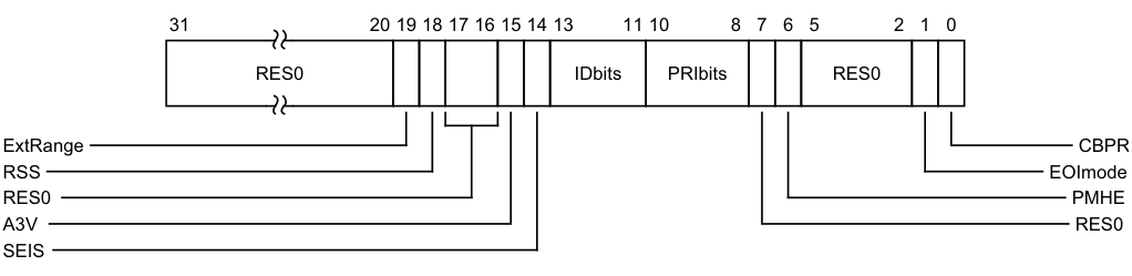
Image text
31 20 19 18 17 16 15 14 13 11 10 8 7 6 5 2 1 0
RES0 IDbits PRIbits RES0
ExtRange CBPR
RSS EOImode
RES0 PMHE
A3V RES0
SEIS
ExtRange, bit [19]
Extended INTID range (read-only).
0b0 CPU interface does not support INTIDs in the range 1024..8191. Behaviour is UNPREDICTABLE if the IRI delivers an interrupt in the range 1024 to 8191 to the CPU interface. Note Arm strongly recommends that the IRI is not configured to deliver interrupts in this range to a PE that does not support them. 0b1 CPU interface supports INTIDs in the range 1024..8191. All INTIDs in the range 1024..8191 are treated as requiring deactivation. If EL3 is implemented, ICC_CTLR_EL1.ExtRange is an alias of ICC_CTLR_EL3.ExtRange.
RSS, bit [18]
Range Selector Support. Possible values are: 0b0 Targeted SGIs with affinity level 0 values of 0 - 15 are supported. 0b1 Targeted SGIs with affinity level 0 values of 0 - 255 are supported. This bit is read-only.
Bits [17:16]
Reserved, RES0.
A3V, bit [15]
Affinity 3 Valid. Read-only and writes are ignored. Possible values are:
0b0 The CPU interface logic only supports zero values of Affinity 3 in SGI generation System registers. 0b1 The CPU interface logic supports non-zero values of Affinity 3 in SGI generation System registers.
If EL3 is implemented and using AArch32, this bit is an alias of ICC_MCTLR.A3V. If EL3 is implemented and using AArch64, this bit is an alias of ICC_CTLR_EL3.A3V.
SEIS, bit [14]
SEI Support. Read-only and writes are ignored. Indicates whether the CPU interface supports local generation of SEIs:
0b0 The CPU interface logic does not support local generation of SEIs. 0b1 The CPU interface logic supports local generation of SEIs. If EL3 is implemented and using AArch32, this bit is an alias of ICC_MCTLR.SEIS.
If EL3 is implemented and using AArch64, this bit is an alias of ICC_CTLR_EL3.SEIS.
IDbits, bits [13:11]
Identifier bits. Read-only and writes are ignored. The number of physical interrupt identifier bits supported:
0b000 16 bits. 0b001 24 bits. All other values are reserved. If EL3 is implemented and using AArch32, this field is an alias of ICC_MCTLR.IDbits. If EL3 is implemented and using AArch64, this field is an alias of ICC_CTLR_EL3.IDbits.
PRIbits, bits [10:8]
Priority bits. Read-only and writes are ignored. The number of priority bits implemented, minus one.
An implementation that supports two Security states must implement at least 32 levels of physical priority (5 priority bits).
An implementation that supports only a single Security state must implement at least 16 levels of physical priority (4 priority bits).
Note
This field always returns the number of priority bits implemented, regardless of the Security state of the access or the value of GICD_CTLR.DS.
The division between group priority and subpriority is defined in the binary point registers ICC_BPR0 and ICC_BPR1.
If EL3 is implemented and using AArch32, physical accesses return the value from ICC_MCTLR.PRIbits.
If EL3 is implemented and using AArch64, physical accesses return the value from ICC_CTLR_EL3.PRIbits.
If EL3 is not implemented, physical accesses return the value from this field.
Bit [7]
Reserved, RES0.
PMHE, bit [6]
Priority Mask Hint Enable. Controls whether the priority mask register is used as a hint for interrupt distribution:
-
0b0 Disables use of ICC_PMR as a hint for interrupt distribution. 0b1 Enables use of ICC_PMR as a hint for interrupt distribution. If EL3 is implemented: • If EL3 is using AArch32, this bit is an alias of ICC_MCTLR.PMHE. • If EL3 is using AArch64, this bit is an alias of ICC_CTLR_EL3.PMHE. • If GICD_CTLR.DS == 0, this bit is read-only. • If GICD_CTLR.DS == 1, this bit is read/write. If EL3 is not implemented, it is IMPLEMENTATION DEFINED whether this bit is read-only or read-write:
-
If this bit is read-only, an implementation can choose to make this field RAZ/WI or RAO/WI.
-
• If this bit is read/write, it resets to zero.
-
Bits [5:2]
Reserved, RES0.
EOImode, bit [1]
EOI mode for the current Security state. Controls whether a write to an End of Interrupt register also deactivates the interrupt:
0b0 ICC_EOIR0 and ICC_EOIR1 provide both priority drop and interrupt deactivation functionality. Accesses to ICC_DIR are UNPREDICTABLE. 0b1 ICC_EOIR0 and ICC_EOIR1 provide priority drop functionality only. ICC_DIR provides interrupt deactivation functionality. If EL3 is implemented:
• If EL3 is using AArch32, this bit is an alias of ICC_MCTLR.EOImode_EL1{S, NS} where S or NS corresponds to the current Security state. • If EL3 is using AArch64, this bit is an alias of ICC_CTLR_EL3.EOImode_EL1{S, NS} where S or NS corresponds to the current Security state. If EL3 is not implemented, it is IMPLEMENTATION DEFINED whether this bit is read-only or read-write:
• If this bit is read-only, an implementation can choose to make this field RAZ/WI or RAO/WI. • If this bit is read/write, it resets to zero. CBPR, bit [0]
Common Binary Point Register. Controls whether the same register is used for interrupt preemption of both Group 0 and Group 1 interrupts:
0b0 ICC_BPR0 determines the preemption group for Group 0 interrupts only. ICC_BPR1 determines the preemption group for Group 1 interrupts. 0b1 ICC_BPR0 determines the preemption group for both Group 0 and Group 1 interrupts. If EL3 is implemented: • If EL3 is using AArch32, this bit is an alias of ICC_MCTLR.CBPR_EL1{S,NS} where S or NS corresponds to the current Security state. • If EL3 is using AArch64, this bit is an alias of ICC_CTLR_EL3.CBPR_EL1{S,NS} where S or NS corresponds to the current Security state. • If GICD_CTLR.DS == 0, this bit is read-only.
-
If GICD_CTLR.DS == 1, this bit is read/write.
-
If EL3 is not implemented, it is IMPLEMENTATION DEFINED whether this bit is read-only or read-write:
-
If this bit is read-only, an implementation can choose to make this field RAZ/WI or RAO/WI.
-
• If this bit is read/write, it resets to zero.
Accessing the ICC_CTLR
Accesses to this register use the following encodings in the System instruction encoding space:
MRC{}{} , {#},
}, {#} ,
| coproc | opc1 | CRn | CRm | opc2 |
|---|---|---|---|---|
| 0b1111 | 0b000 | 0b1100 | 0b1100 | 0b100 |
if PSTATE.EL == EL0 then UNDEFINED;
elsif PSTATE.EL == EL1 then
if Halted() && HaveEL(EL3) && EDSCR.SDD == '1' &&
boolean IMPLEMENTATION_DEFINED "EL3 trap priority
when SDD == '1'" && !ELUsingAArch32(EL3) && SCR_EL3.<IRQ,FIQ> == '11' then UNDEFINED;
elsif Halted() && HaveEL(EL3) && EDSCR.SDD == '1' &&
boolean IMPLEMENTATION_DEFINED "EL3 trap priority
when SDD == '1'" && ELUsingAArch32(EL3) && PSTATE.M != M32_Monitor && SCR.<IRQ,FIQ> == '11' then UNDEFINED;
elsif EL2Enabled() && !ELUsingAArch32(EL2) && HSTR_EL2.T12 == '1' then AArch64.AArch32SystemAccessTrap(EL2, 0x03);
elsif EL2Enabled() && ELUsingAArch32(EL2) && HSTR.T12 == '1' then AArch32.TakeHypTrapException(0x03);
elsif EL2Enabled() && !ELUsingAArch32(EL2) && ICH_HCR_EL2.TC == '1' then AArch64.AArch32SystemAccessTrap(EL2, 0x03);
elsif EL2Enabled() && ELUsingAArch32(EL2) && ICH_HCR.TC == '1' then AArch32.TakeHypTrapException(0x03);
elsif EL2Enabled() && !ELUsingAArch32(EL2) && HCR_EL2.FMO == '1' then
return ICV_CTLR;
elsif EL2Enabled() && !ELUsingAArch32(EL2) && HCR_EL2.IMO == '1' then
return ICV_CTLR;
elsif EL2Enabled() && ELUsingAArch32(EL2) && HCR.FMO == '1' then
return ICV_CTLR;
elsif EL2Enabled() && ELUsingAArch32(EL2) && HCR.IMO == '1' then
return ICV_CTLR;
elsif HaveEL(EL3) && !ELUsingAArch32(EL3) && SCR_EL3.<IRQ,FIQ> == '11' then
if Halted() && EDSCR.SDD == '1' then UNDEFINED;
else AArch64.AArch32SystemAccessTrap(EL3, 0x03);
elsif HaveEL(EL3) && ELUsingAArch32(EL3) && PSTATE.M != M32_Monitor && SCR.<IRQ,FIQ> == '11' then
if Halted() && EDSCR.SDD == '1' then UNDEFINED;
else AArch32.TakeMonitorTrapException();
elsif HaveEL(EL3) then
return ICC_CTLR_NS;
else return ICC_CTLR;
elsif PSTATE.EL == EL2 then
if Halted() && HaveEL(EL3) && EDSCR.SDD == '1' &&
boolean IMPLEMENTATION_DEFINED "EL3 trap priority
when SDD == '1'" && !ELUsingAArch32(EL3) && SCR_EL3.<IRQ,FIQ> == '11' then UNDEFINED;
elsif Halted() && HaveEL(EL3) && EDSCR.SDD == '1' &&
boolean IMPLEMENTATION_DEFINED "EL3 trap priority
when SDD == '1'" && ELUsingAArch32(EL3) && SCR.<IRQ,FIQ> == '11' then UNDEFINED;
elsif ICC_HSRE.SRE == '0' then
UNDEFINED;
elsif HaveEL(EL3) && !ELUsingAArch32(EL3) && SCR_EL3.<IRQ,FIQ> == '11'
then if Halted() && EDSCR.SDD == '1'
then UNDEFINED;
else AArch64.AArch32SystemAccessTrap(EL3, 0x03);
elsif HaveEL(EL3) && ELUsingAArch32(EL3) && SCR.<IRQ,FIQ> == '11'
then if Halted() && EDSCR.SDD == '1'
then UNDEFINED;
else AArch32.TakeMonitorTrapException();
elsif HaveEL(EL3)
then return ICC_CTLR_NS;
else return ICC_CTLR;
elsif PSTATE.EL == EL3
then if ICC_MSRE.SRE == '0'
then UNDEFINED;
else if SCR.NS == '0'
then return ICC_CTLR_S;
else return ICC_CTLR_NS;
MCR{}{} , {#},
}, {#} ,
| coproc | opc1 | CRn | CRm | opc2 |
|---|---|---|---|---|
| 0b1111 | 0b000 | 0b1100 | 0b1100 | 0b100 |
if PSTATE.EL == EL0 then UNDEFINED;
elsif PSTATE.EL == EL1 then
if Halted() && HaveEL(EL3) && EDSCR.SDD == '1' &&
boolean IMPLEMENTATION_DEFINED "EL3 trap priority
when SDD == '1'" && !ELUsingAArch32(EL3) && SCR_EL3.<IRQ,FIQ> == '11' then UNDEFINED;
elsif Halted() && HaveEL(EL3) && EDSCR.SDD == '1' &&
boolean IMPLEMENTATION_DEFINED "EL3 trap priority
when SDD == '1'" && ELUsingAArch32(EL3) && PSTATE.M != M32_Monitor && SCR.<IRQ,FIQ> == '11' then UNDEFINED;
elsif EL2Enabled() && !ELUsingAArch32(EL2) && HSTR_EL2.T12 == '1' then AArch64.AArch32SystemAccessTrap(EL2, 0x03);
elsif EL2Enabled() && ELUsingAArch32(EL2) && HSTR.T12 == '1' then AArch32.TakeHypTrapException(0x03);
elsif EL2Enabled() && !ELUsingAArch32(EL2) && ICH_HCR_EL2.TC == '1' then AArch64.AArch32SystemAccessTrap(EL2, 0x03);
elsif EL2Enabled() && ELUsingAArch32(EL2) && ICH_HCR.TC == '1' then AArch32.TakeHypTrapException(0x03);
elsif EL2Enabled() && !ELUsingAArch32(EL2) && HCR_EL2.FMO == '1' then ICV_CTLR = R[t];
elsif EL2Enabled() && !ELUsingAArch32(EL2) && HCR_EL2.IMO == '1' then ICV_CTLR = R[t];
elsif EL2Enabled() && ELUsingAArch32(EL2) && HCR.FMO == '1' then ICV_CTLR = R[t];
elsif EL2Enabled() && ELUsingAArch32(EL2) && HCR.IMO == '1' then ICV_CTLR = R[t];
elsif HaveEL(EL3) && !ELUsingAArch32(EL3) && SCR_EL3.<IRQ,FIQ> == '11' then
if Halted() && EDSCR.SDD == '1' then UNDEFINED;
else AArch64.AArch32SystemAccessTrap(EL3, 0x03);
elsif HaveEL(EL3) && ELUsingAArch32(EL3) && PSTATE.M != M32_Monitor && SCR.<IRQ,FIQ> == '11' then
if Halted() && EDSCR.SDD == '1' then UNDEFINED;
else AArch32.TakeMonitorTrapException();
elsif HaveEL(EL3) then ICC_CTLR_NS = R[t];
else ICC_CTLR = R[t];
elsif PSTATE.EL == EL2 then
if Halted() && HaveEL(EL3) && EDSCR.SDD == '1' &&
boolean IMPLEMENTATION_DEFINED "EL3 trap priority
when SDD == '1'" && !ELUsingAArch32(EL3) && SCR_EL3.<IRQ,FIQ> == '11' then UNDEFINED;
elsif Halted() && HaveEL(EL3) && EDSCR.SDD == '1' &&
boolean IMPLEMENTATION_DEFINED "EL3 trap priority
when SDD == '1'" && ELUsingAArch32(EL3) && SCR.<IRQ,FIQ> == '11' then UNDEFINED;
elsif ICC_HSRE.SRE == '0' then UNDEFINED;
elsif HaveEL(EL3) && !ELUsingAArch32(EL3) && SCR_EL3.<IRQ,FIQ> == '11' then
if Halted() && EDSCR.SDD == '1' then UNDEFINED;
else AArch64.AArch32SystemAccessTrap(EL3, 0x03);
elsif HaveEL(EL3) && ELUsingAArch32(EL3) && SCR.<IRQ,FIQ> == '11' then
if Halted() && EDSCR.SDD == '1' then UNDEFINED;
else AArch32.TakeMonitorTrapException();
elsif HaveEL(EL3) then ICC_CTLR_NS = R[t];
else ICC_CTLR = R[t];
elsif PSTATE.EL == EL3 then
if ICC_MSRE.SRE == '0' then UNDEFINED;
else if SCR.NS == '0' then ICC_CTLR_S = R[t];
else ICC_CTLR_NS = R[t];
12.5.7 ICC_DIR, Interrupt Controller Deactivate Interrupt Register
The ICC_DIR characteristics are:
Purpose
When interrupt priority drop is separated from interrupt deactivation, a write to this register deactivates the specified interrupt.
Configurations
AArch32 System register ICC_DIR performs the same function as AArch64 System register ICC_DIR_EL1.
This register is present only when AArch32 is supported at any Exception level. Otherwise, direct accesses to ICC_DIR are UNDEFINED.
Attributes
ICC_DIR is a 32-bit register.
Field descriptions
The ICC_DIR bit assignments are:
| | 31 | | 24 | 23 | | 0 | | |—|—|—|—|—|—|—| |||||||||
Bits [31:24]
Reserved, RES0.
INTID, bits [23:0]
The INTID of the interrupt to be deactivated.
This field has either 16 or 24 bits implemented. The number of implemented bits can be found in ICC_CTLR.IDbits and ICC_MCTLR.IDbits. If only 16 bits are implemented, bits [23:16] of this register are RES0.
Accessing the ICC_DIR
There are two cases when writing to ICC_DIR_EL1 that were UNPREDICTABLE for a corresponding GICv2 write to GICC_DIR:
-
When EOImode == 0. GICv3 implementations must ignore such writes. In systems supporting system error generation, an implementation might generate an SEI.
-
When EOImode == 1 but no EOI has been issued. The interrupt will be de-activated by the Distributor, however the active priority in the CPU interface for the interrupt will remain set (because no EOI was issued).
Accesses to this register use the following encodings in the System instruction encoding space:
MCR{}{} , {#},
}, {#} ,
| coproc | opc1 | CRn | CRm | opc2 |
|---|---|---|---|---|
| 0b1111 | 0b000 | 0b1100 | 0b1011 | 0b001 |
if PSTATE.EL == EL0 then UNDEFINED;
elsif PSTATE.EL == EL1 then
if Halted() && HaveEL(EL3) && EDSCR.SDD == '1' &&
boolean IMPLEMENTATION_DEFINED "EL3 trap priority
when SDD == '1'" && !ELUsingAArch32(EL3) && SCR_EL3.<IRQ,FIQ> == '11' then UNDEFINED;
elsif Halted() && HaveEL(EL3) && EDSCR.SDD == '1' &&
boolean IMPLEMENTATION_DEFINED "EL3 trap priority
when SDD == '1'" && ELUsingAArch32(EL3) && PSTATE.M != M32_Monitor && SCR.<IRQ,FIQ> == '11' then UNDEFINED;
elsif EL2Enabled() && !ELUsingAArch32(EL2) && HSTR_EL2.T12 == '1' then AArch64.AArch32SystemAccessTrap(EL2, 0x03);
elsif EL2Enabled() && ELUsingAArch32(EL2) && HSTR.T12 == '1' then AArch32.TakeHypTrapException(0x03);
elsif EL2Enabled() && !ELUsingAArch32(EL2) && ICH_HCR_EL2.TDIR == '1' then AArch64.AArch32SystemAccessTrap(EL2, 0x03);
elsif EL2Enabled() && !ELUsingAArch32(EL2) && ICH_HCR_EL2.TC == '1' then AArch64.AArch32SystemAccessTrap(EL2, 0x03);
elsif EL2Enabled() && ELUsingAArch32(EL2) && ICH_HCR.TC == '1' then AArch32.TakeHypTrapException(0x03);
elsif EL2Enabled() && ELUsingAArch32(EL2) && ICH_HCR.TDIR == '1' then AArch32.TakeHypTrapException(0x03);
elsif EL2Enabled() && !ELUsingAArch32(EL2) && HCR_EL2.FMO == '1' then ICV_DIR = R[t];
elsif EL2Enabled() && !ELUsingAArch32(EL2) && HCR_EL2.IMO == '1' then ICV_DIR = R[t];
elsif EL2Enabled() && ELUsingAArch32(EL2) && HCR.FMO == '1' then ICV_DIR = R[t];
elsif EL2Enabled() && ELUsingAArch32(EL2) && HCR.IMO == '1' then ICV_DIR = R[t];
elsif HaveEL(EL3) && !ELUsingAArch32(EL3) && SCR_EL3.<IRQ,FIQ> == '11' then
if Halted() && EDSCR.SDD == '1' then UNDEFINED;
else AArch64.AArch32SystemAccessTrap(EL3, 0x03);
elsif HaveEL(EL3) && ELUsingAArch32(EL3) && PSTATE.M != M32_Monitor && SCR.<IRQ,FIQ> == '11' then
if Halted() && EDSCR.SDD == '1' then UNDEFINED;
else AArch32.TakeMonitorTrapException();
else ICC_DIR = R[t];
elsif PSTATE.EL == EL2 then
if Halted() && HaveEL(EL3) && EDSCR.SDD == '1' &&
boolean IMPLEMENTATION_DEFINED "EL3 trap priority
when SDD == '1'" && !ELUsingAArch32(EL3) && SCR_EL3.<IRQ,FIQ> == '11' then UNDEFINED;
elsif Halted() && HaveEL(EL3) && EDSCR.SDD == '1' &&
boolean IMPLEMENTATION_DEFINED "EL3 trap priority
when SDD == '1'" && ELUsingAArch32(EL3) && SCR.<IRQ,FIQ> == '11' then UNDEFINED;
elsif ICC_HSRE.SRE == '0' then UNDEFINED;
elsif HaveEL(EL3) && !ELUsingAArch32(EL3) && SCR_EL3.<IRQ,FIQ> == '11' then
if Halted() && EDSCR.SDD == '1' then UNDEFINED;
else AArch64.AArch32SystemAccessTrap(EL3, 0x03);
elsif HaveEL(EL3) && ELUsingAArch32(EL3) && SCR.<IRQ,FIQ> == '11' then
if Halted() && EDSCR.SDD == '1' then UNDEFINED;
else AArch32.TakeMonitorTrapException();
else ICC_DIR = R[t];
elsif PSTATE.EL == EL3 then
if ICC_MSRE.SRE == '0' then UNDEFINED;
else ICC_DIR = R[t];
12.5.8 ICC_EOIR0, Interrupt Controller End Of Interrupt Register 0
The ICC_EOIR0 characteristics are:
Purpose
A PE writes to this register to inform the CPU interface that it has completed the processing of the specified Group 0 interrupt.
Configurations
AArch32 System register ICC_EOIR0 performs the same function as AArch64 System register ICC_EOIR0_EL1.
This register is present only when AArch32 is supported at any Exception level. Otherwise, direct accesses to ICC_EOIR0 are UNDEFINED.
Attributes
ICC_EOIR0 is a 32-bit register.
Field descriptions
The ICC_EOIR0 bit assignments are:
| | 31 | | 24 | 23 | | 0 | | |—|—|—|—|—|—|—| |||||||||
Bits [31:24]
Reserved, RES0.
INTID, bits [23:0]
The INTID from the corresponding ICC_IAR0 access.
This field has either 16 or 24 bits implemented. The number of implemented bits can be found in ICC_CTLR.IDbits and ICC_MCTLR.IDbits. If only 16 bits are implemented, bits [23:16] of this register are RES0.
If the EOImode bit for the current Exception level and Security state is 0, a write to this register drops the priority for the interrupt, and also deactivates the interrupt.
If the EOImode bit for the current Exception level and Security state is 1, a write to this register only drops the priority for the interrupt. Software must write to ICC_DIR to deactivate the interrupt. The appropriate EOImode bit varies as follows:
-
If EL3 is not implemented, the appropriate bit is ICC_CTLR.EOImode.
-
If EL3 is implemented and the software is executing in Monitor mode, the appropriate bit is ICC_MCTLR.EOImode_EL3.
-
If EL3 is implemented and the software is not executing in Monitor mode, the bit depends on the current Security state:
-
If the software is executing in Secure state, the bit is ICC_CTLR.EOImode in the Secure instance of ICC_CTLR. This is an alias of ICC_MCTLR.EOImode_EL1S.
-
If the software is executing in Non-secure state, the bit is ICC_CTLR.EOImode in the Non-secure instance of ICC_CTLR. This is an alias of ICC_MCTLR.EOImode_EL1NS.
-
Accessing the ICC_EOIR0
A write to this register must correspond to the most recent valid read by this PE from an Interrupt Acknowledge Register, and must correspond to the INTID that was read from ICC_IAR0, otherwise the system behavior is UNPREDICTABLE. A valid read is a read that returns a valid INTID that is not a special INTID.
A write of a Special INTID is ignored. For more information, see Special INTIDs.
Accesses to this register use the following encodings in the System instruction encoding space:
MCR{}{} , {#},
}, {#} ,
| coproc | opc1 | CRn | CRm | opc2 |
|---|---|---|---|---|
| 0b1111 | 0b000 | 0b1100 | 0b1000 | 0b001 |
if PSTATE.EL == EL0 then UNDEFINED;
elsif PSTATE.EL == EL1 then
if Halted() && HaveEL(EL3) && EDSCR.SDD == '1' &&
boolean IMPLEMENTATION_DEFINED "EL3 trap priority
when SDD == '1'" && !ELUsingAArch32(EL3) && SCR_EL3.FIQ == '1' then UNDEFINED;
elsif Halted() && HaveEL(EL3) && EDSCR.SDD == '1' &&
boolean IMPLEMENTATION_DEFINED "EL3 trap priority
when SDD == '1'" && ELUsingAArch32(EL3) && PSTATE.M != M32_Monitor && SCR.FIQ == '1' then UNDEFINED;
elsif EL2Enabled() && !ELUsingAArch32(EL2) && HSTR_EL2.T12 == '1' then AArch64.AArch32SystemAccessTrap(EL2, 0x03);
elsif EL2Enabled() && ELUsingAArch32(EL2) && HSTR.T12 == '1' then AArch32.TakeHypTrapException(0x03);
elsif ICC_SRE.SRE == '0' then UNDEFINED;
elsif EL2Enabled() && !ELUsingAArch32(EL2) && ICH_HCR_EL2.TALL0 == '1' then AArch64.AArch32SystemAccessTrap(EL2, 0x03);
elsif EL2Enabled() && ELUsingAArch32(EL2) && ICH_HCR.TALL0 == '1' then AArch32.TakeHypTrapException(0x03);
elsif EL2Enabled() && !ELUsingAArch32(EL2) && HCR_EL2.FMO == '1' then ICV_EOIR0 = R[t];
elsif EL2Enabled() && ELUsingAArch32(EL2) && HCR.FMO == '1' then ICV_EOIR0 = R[t];
elsif HaveEL(EL3) && !ELUsingAArch32(EL3) && SCR_EL3.FIQ == '1' then
if Halted() && EDSCR.SDD == '1' then UNDEFINED;
else AArch64.AArch32SystemAccessTrap(EL3, 0x03);
elsif HaveEL(EL3) && ELUsingAArch32(EL3) && PSTATE.M != M32_Monitor && SCR.FIQ == '1' then
if Halted() && EDSCR.SDD == '1' then UNDEFINED;
else AArch32.TakeMonitorTrapException();
else ICC_EOIR0 = R[t];
elsif PSTATE.EL == EL2 then
if Halted() && HaveEL(EL3) && EDSCR.SDD == '1' &&
boolean IMPLEMENTATION_DEFINED "EL3 trap priority
when SDD == '1'" && !ELUsingAArch32(EL3) && SCR_EL3.FIQ == '1' then UNDEFINED;
elsif Halted() && HaveEL(EL3) && EDSCR.SDD == '1' &&
boolean IMPLEMENTATION_DEFINED "EL3 trap priority
when SDD == '1'" && ELUsingAArch32(EL3) && SCR.FIQ == '1' then UNDEFINED;
elsif ICC_HSRE.SRE == '0' then UNDEFINED;
elsif HaveEL(EL3) && !ELUsingAArch32(EL3) && SCR_EL3.FIQ == '1' then
if Halted() && EDSCR.SDD == '1' then UNDEFINED;
else AArch64.AArch32SystemAccessTrap(EL3, 0x03);
elsif HaveEL(EL3) && ELUsingAArch32(EL3) && SCR.FIQ == '1' then
if Halted() && EDSCR.SDD == '1' then UNDEFINED;
else AArch32.TakeMonitorTrapException();
else ICC_EOIR0 = R[t];
elsif PSTATE.EL == EL3 then
if ICC_MSRE.SRE == '0' then UNDEFINED;
else ICC_EOIR0 = R[t];
12.5.9 ICC_EOIR1, Interrupt Controller End Of Interrupt Register 1
The ICC_EOIR1 characteristics are:
Purpose
A PE writes to this register to inform the CPU interface that it has completed the processing of the specified Group 1 interrupt.
Configurations
AArch32 System register ICC_EOIR1 performs the same function as AArch64 System register ICC_EOIR1_EL1.
This register is present only when AArch32 is supported at any Exception level. Otherwise, direct accesses to ICC_EOIR1 are UNDEFINED.
Attributes
ICC_EOIR1 is a 32-bit register.
Field descriptions
The ICC_EOIR1 bit assignments are:
| | 31 | | 24 | 23 | | 0 | | |—|—|—|—|—|—|—| |||||||||
Bits [31:24]
Reserved, RES0.
INTID, bits [23:0]
The INTID from the corresponding ICC_IAR1 access.
This field has either 16 or 24 bits implemented. The number of implemented bits can be found in ICC_CTLR.IDbits and ICC_MCTLR.IDbits. If only 16 bits are implemented, bits [23:16] of this register are RES0.
If the EOImode bit for the current Exception level and Security state is 0, a write to this register drops the priority for the interrupt, and also deactivates the interrupt.
If the EOImode bit for the current Exception level and Security state is 1, a write to this register only drops the priority for the interrupt. Software must write to ICC_DIR to deactivate the interrupt.
The appropriate EOImode bit varies as follows:
-
If EL3 is not implemented, the appropriate bit is ICC_CTLR.EOImode.
-
If EL3 is implemented and the software is executing in Monitor mode, the appropriate bit is ICC_MCTLR.EOImode_EL3.
-
If EL3 is implemented and the software is not executing in Monitor mode, the bit depends on the current Security state:
-
If the software is executing in Secure state, the bit is ICC_CTLR.EOImode in the Secure instance of ICC_CTLR. This is an alias of ICC_MCTLR.EOImode_EL1S.
-
If the software is executing in Non-secure state, the bit is ICC_CTLR.EOImode in the Non-secure instance of ICC_CTLR. This is an alias of ICC_MCTLR.EOImode_EL1NS.
-
Accessing the ICC_EOIR1
A write to this register must correspond to the most recent valid read by this PE from an Interrupt Acknowledge Register, and must correspond to the INTID that was read from ICC_IAR1, otherwise the system behavior is UNPREDICTABLE. A valid read is a read that returns a valid INTID that is not a special INTID.
A write of a Special INTID is ignored. For more information, see Special INTIDs.
Accesses to this register use the following encodings in the System instruction encoding space:
MCR{}{} , {#},
}, {#} ,
| coproc | opc1 | CRn | CRm | opc2 |
|---|---|---|---|---|
| 0b1111 | 0b000 | 0b1100 | 0b1100 | 0b001 |
if PSTATE.EL == EL0 then UNDEFINED;
elsif PSTATE.EL == EL1 then
if Halted() && HaveEL(EL3) && EDSCR.SDD == '1' &&
boolean IMPLEMENTATION_DEFINED "EL3 trap priority
when SDD == '1'" && !ELUsingAArch32(EL3) && SCR_EL3.IRQ == '1' then UNDEFINED;
elsif Halted() && HaveEL(EL3) && EDSCR.SDD == '1' &&
boolean IMPLEMENTATION_DEFINED "EL3 trap priority
when SDD == '1'" && ELUsingAArch32(EL3) && PSTATE.M != M32_Monitor && SCR.IRQ == '1' then UNDEFINED;
elsif EL2Enabled() && !ELUsingAArch32(EL2) && HSTR_EL2.T12 == '1' then AArch64.AArch32SystemAccessTrap(EL2, 0x03);
elsif EL2Enabled() && ELUsingAArch32(EL2) && HSTR.T12 == '1' then AArch32.TakeHypTrapException(0x03);
elsif ICC_SRE.SRE == '0' then UNDEFINED;
elsif EL2Enabled() && !ELUsingAArch32(EL2) && ICH_HCR_EL2.TALL1 == '1' then AArch64.AArch32SystemAccessTrap(EL2, 0x03);
elsif EL2Enabled() && ELUsingAArch32(EL2) && ICH_HCR.TALL1 == '1' then AArch32.TakeHypTrapException(0x03);
elsif EL2Enabled() && !ELUsingAArch32(EL2) && HCR_EL2.IMO == '1' then ICV_EOIR1 = R[t];
elsif EL2Enabled() && ELUsingAArch32(EL2) && HCR.IMO == '1' then ICV_EOIR1 = R[t];
elsif HaveEL(EL3) && !ELUsingAArch32(EL3) && SCR_EL3.IRQ == '1' then
if Halted() && EDSCR.SDD == '1' then UNDEFINED;
else AArch64.AArch32SystemAccessTrap(EL3, 0x03);
elsif HaveEL(EL3) && ELUsingAArch32(EL3) && PSTATE.M != M32_Monitor && SCR.IRQ == '1' then
if Halted() && EDSCR.SDD == '1' then UNDEFINED;
else AArch32.TakeMonitorTrapException();
else ICC_EOIR1 = R[t];
elsif PSTATE.EL == EL2 then
if Halted() && HaveEL(EL3) && EDSCR.SDD == '1' &&
boolean IMPLEMENTATION_DEFINED "EL3 trap priority
when SDD == '1'" && !ELUsingAArch32(EL3) && SCR_EL3.IRQ == '1' then UNDEFINED;
elsif Halted() && HaveEL(EL3) && EDSCR.SDD == '1' &&
boolean IMPLEMENTATION_DEFINED "EL3 trap priority
when SDD == '1'" && ELUsingAArch32(EL3) && SCR.IRQ == '1' then UNDEFINED;
elsif ICC_HSRE.SRE == '0' then UNDEFINED;
elsif HaveEL(EL3) && !ELUsingAArch32(EL3) && SCR_EL3.IRQ == '1' then
if Halted() && EDSCR.SDD == '1' then UNDEFINED;
else AArch64.AArch32SystemAccessTrap(EL3, 0x03);
elsif HaveEL(EL3) && ELUsingAArch32(EL3) && SCR.IRQ == '1' then
if Halted() && EDSCR.SDD == '1' then UNDEFINED;
else AArch32.TakeMonitorTrapException();
else ICC_EOIR1 = R[t];
elsif PSTATE.EL == EL3 then
if ICC_MSRE.SRE == '0' then UNDEFINED;
else ICC_EOIR1 = R[t];
12.5.10 ICC_HPPIR0, Interrupt Controller Highest Priority Pending Interrupt Register 0
The ICC_HPPIR0 characteristics are:
Purpose
Indicates the highest priority pending Group 0 interrupt on the CPU interface.
Configurations
AArch32 System register ICC_HPPIR0 performs the same function as AArch64 System register ICC_HPPIR0_EL1.
This register is present only when AArch32 is supported at any Exception level. Otherwise, direct accesses to ICC_HPPIR0 are UNDEFINED.
Attributes
ICC_HPPIR0 is a 32-bit register.
Field descriptions
The ICC_HPPIR0 bit assignments are:

31 24 23 0
RES0 INTID
Bits [31:24]
Reserved, RES0.
INTID, bits [23:0]
The INTID of the highest priority pending interrupt, if that interrupt is observable at the current Security state and Exception level.
If the highest priority pending interrupt is not observable, this field contains a special INTID to indicate the reason. These special INTIDs can be one of: 1020, 1021, or 1023. For more information, see Special INTIDs.
This field has either 16 or 24 bits implemented. The number of implemented bits can be found in ICC_CTLR.IDbits and ICC_MCTLR.IDbits. If only 16 bits are implemented, bits [23:16] of this register are RES0.
Accessing the ICC_HPPIR0
Accesses to this register use the following encodings in the System instruction encoding space:
MRC{}{} , {#},
}, {#} ,
| coproc | opc1 | CRn | CRm | opc2 |
|---|---|---|---|---|
| 0b1111 | 0b000 | 0b1100 | 0b1000 | 0b010 |
if PSTATE.EL == EL0 then UNDEFINED;
elsif PSTATE.EL == EL1 then
if Halted() && HaveEL(EL3) && EDSCR.SDD == '1' &&
boolean IMPLEMENTATION_DEFINED "EL3 trap priority
when SDD == '1'" && !ELUsingAArch32(EL3) && SCR_EL3.FIQ == '1' then
UNDEFINED;
elsif Halted() && HaveEL(EL3) && EDSCR.SDD == '1' &&
boolean IMPLEMENTATION_DEFINED "EL3 trap priority when SDD == '1'" && ELUsingAArch32(EL3) && PSTATE.M != M32_Monitor && SCR.FIQ == '1' then
UNDEFINED;
elsif EL2Enabled() && !ELUsingAArch32(EL2) && HSTR_EL2.T12 == '1'
then AArch64.AArch32SystemAccessTrap(EL2, 0x03);
elsif EL2Enabled() && ELUsingAArch32(EL2) && HSTR.T12 == '1'
then AArch32.TakeHypTrapException(0x03);
elsif ICC_SRE.SRE == '0'
then UNDEFINED;
elsif EL2Enabled() && !ELUsingAArch32(EL2) && ICH_HCR_EL2.TALL0 == '1'
then AArch64.AArch32SystemAccessTrap(EL2, 0x03);
elsif EL2Enabled() && ELUsingAArch32(EL2) && ICH_HCR.TALL0 == '1'
then AArch32.TakeHypTrapException(0x03);
elsif EL2Enabled() && !ELUsingAArch32(EL2) && HCR_EL2.FMO == '1'
then return ICV_HPPIR0;
elsif EL2Enabled() && ELUsingAArch32(EL2) && HCR.FMO == '1'
then return ICV_HPPIR0;
elsif HaveEL(EL3) && !ELUsingAArch32(EL3) && SCR_EL3.FIQ == '1'
then if Halted() && EDSCR.SDD == '1'
then UNDEFINED;
else AArch64.AArch32SystemAccessTrap(EL3, 0x03);
elsif HaveEL(EL3) && ELUsingAArch32(EL3) && PSTATE.M != M32_Monitor && SCR.FIQ == '1'
then if Halted() && EDSCR.SDD == '1'
then UNDEFINED;
else AArch32.TakeMonitorTrapException();
else return ICC_HPPIR0;
elsif PSTATE.EL == EL2
then
if Halted() && HaveEL(EL3) && EDSCR.SDD == '1' &&
boolean IMPLEMENTATION_DEFINED "EL3 trap priority when SDD == '1'" && !ELUsingAArch32(EL3) && SCR_EL3.FIQ == '1'
then UNDEFINED;
elsif Halted() && HaveEL(EL3) && EDSCR.SDD == '1' &&
boolean IMPLEMENTATION_DEFINED "EL3 trap priority when SDD == '1'" && ELUsingAArch32(EL3) && SCR.FIQ == '1'
then UNDEFINED;
elsif ICC_HSRE.SRE == '0'
then UNDEFINED;
elsif HaveEL(EL3) && !ELUsingAArch32(EL3) && SCR_EL3.FIQ == '1'
then if Halted() && EDSCR.SDD == '1'
then UNDEFINED;
else AArch64.AArch32SystemAccessTrap(EL3, 0x03);
elsif HaveEL(EL3) && ELUsingAArch32(EL3) && SCR.FIQ == '1'
then if Halted() && EDSCR.SDD == '1'
then UNDEFINED;
else AArch32.TakeMonitorTrapException();
else return ICC_HPPIR0;
elsif PSTATE.EL == EL3
then if ICC_MSRE.SRE == '0'
then UNDEFINED;
else return ICC_HPPIR0;
12.5.11 ICC_HPPIR1, Interrupt Controller Highest Priority Pending Interrupt Register 1
The ICC_HPPIR1 characteristics are:
Purpose
Indicates the highest priority pending Group 1 interrupt on the CPU interface.
Configurations
AArch32 System register ICC_HPPIR1 performs the same function as AArch64 System register ICC_HPPIR1_EL1.
This register is present only when AArch32 is supported at any Exception level. Otherwise, direct accesses to ICC_HPPIR1 are UNDEFINED.
Attributes
ICC_HPPIR1 is a 32-bit register.
Field descriptions
The ICC_HPPIR1 bit assignments are:

31 24 23 0
RES0 INTID
Bits [31:24]
Reserved, RES0.
INTID, bits [23:0]
The INTID of the highest priority pending interrupt, if that interrupt is observable at the current Security state and Exception level.
If the highest priority pending interrupt is not observable, this field contains a special INTID to indicate the reason. This special INTID can take the value 1023 only. For more information, see Special INTIDs.
This field has either 16 or 24 bits implemented. The number of implemented bits can be found in ICC_CTLR.IDbits and ICC_MCTLR.IDbits. If only 16 bits are implemented, bits [23:16] of this register are RES0.
Accessing the ICC_HPPIR1
Accesses to this register use the following encodings in the System instruction encoding space:
MRC{}{} , {#},
}, {#} ,
| coproc | opc1 | CRn | CRm | opc2 |
|---|---|---|---|---|
| 0b1111 | 0b000 | 0b1100 | 0b1100 | 0b010 |
if PSTATE.EL == EL0 then UNDEFINED;
elsif PSTATE.EL == EL1 then
if Halted() && HaveEL(EL3) && EDSCR.SDD == '1' &&
boolean IMPLEMENTATION_DEFINED "EL3 trap priority
when SDD == '1'" && !ELUsingAArch32(EL3) && SCR_EL3.IRQ == '1' then
UNDEFINED;
elsif Halted() && HaveEL(EL3) && EDSCR.SDD == '1' &&
boolean IMPLEMENTATION_DEFINED "EL3 trap priority when SDD == '1'" && ELUsingAArch32(EL3) && PSTATE.M != M32_Monitor && SCR.IRQ == '1' then
UNDEFINED;
elsif EL2Enabled() && !ELUsingAArch32(EL2) && HSTR_EL2.T12 == '1'
then AArch64.AArch32SystemAccessTrap(EL2, 0x03);
elsif EL2Enabled() && ELUsingAArch32(EL2) && HSTR.T12 == '1'
then AArch32.TakeHypTrapException(0x03);
elsif ICC_SRE.SRE == '0'
then UNDEFINED;
elsif EL2Enabled() && !ELUsingAArch32(EL2) && ICH_HCR_EL2.TALL1 == '1'
then AArch64.AArch32SystemAccessTrap(EL2, 0x03);
elsif EL2Enabled() && ELUsingAArch32(EL2) && ICH_HCR.TALL1 == '1'
then AArch32.TakeHypTrapException(0x03);
elsif EL2Enabled() && !ELUsingAArch32(EL2) && HCR_EL2.IMO == '1'
then return ICV_HPPIR1;
elsif EL2Enabled() && ELUsingAArch32(EL2) && HCR.IMO == '1'
then return ICV_HPPIR1;
elsif HaveEL(EL3) && !ELUsingAArch32(EL3) && SCR_EL3.IRQ == '1'
then if Halted() && EDSCR.SDD == '1'
then UNDEFINED;
else AArch64.AArch32SystemAccessTrap(EL3, 0x03);
elsif HaveEL(EL3) && ELUsingAArch32(EL3) && PSTATE.M != M32_Monitor && SCR.IRQ == '1'
then if Halted() && EDSCR.SDD == '1'
then UNDEFINED;
else AArch32.TakeMonitorTrapException();
else return ICC_HPPIR1;
elsif PSTATE.EL == EL2
then
if Halted() && HaveEL(EL3) && EDSCR.SDD == '1' &&
boolean IMPLEMENTATION_DEFINED "EL3 trap priority when SDD == '1'" && !ELUsingAArch32(EL3) && SCR_EL3.IRQ == '1'
then UNDEFINED;
elsif Halted() && HaveEL(EL3) && EDSCR.SDD == '1' &&
boolean IMPLEMENTATION_DEFINED "EL3 trap priority when SDD == '1'" && ELUsingAArch32(EL3) && SCR.IRQ == '1'
then UNDEFINED;
elsif ICC_HSRE.SRE == '0'
then UNDEFINED;
elsif HaveEL(EL3) && !ELUsingAArch32(EL3) && SCR_EL3.IRQ == '1'
then if Halted() && EDSCR.SDD == '1'
then UNDEFINED;
else AArch64.AArch32SystemAccessTrap(EL3, 0x03);
elsif HaveEL(EL3) && ELUsingAArch32(EL3) && SCR.IRQ == '1'
then if Halted() && EDSCR.SDD == '1'
then UNDEFINED;
else AArch32.TakeMonitorTrapException();
else return ICC_HPPIR1;
elsif PSTATE.EL == EL3
then if ICC_MSRE.SRE == '0'
then UNDEFINED;
else return ICC_HPPIR1;
12.5.12 ICC_HSRE, Interrupt Controller Hyp System Register Enable register
The ICC_HSRE characteristics are:
Purpose
Controls whether the System register interface or the memory-mapped interface to the GIC CPU interface is used for EL2.
Configurations
AArch32 System register ICC_HSRE bits [31:0] are architecturally mapped to AArch64 System register ICC_SRE_EL2[31:0].
This register is present only when AArch32 is supported at any Exception level. Otherwise, direct accesses to ICC_HSRE are UNDEFINED.
Attributes
ICC_HSRE is a 32-bit register.
Field descriptions
The ICC_HSRE bit assignments are:

Image text
31 4 3 2 1 0
RES0
SRE
DFB
DIB
Enable
Enable, bit [3]
Enable. Enables lower Exception level access to ICC_SRE.
0b0 Non-secure EL1 accesses to ICC_SRE trap to EL2. 0b1 Non-secure EL1 accesses to ICC_SRE do not trap to EL2.
If ICC_HSRE.SRE is RAO/WI, an implementation is permitted to make the Enable bit RAO/WI.
If ICC_HSRE.SRE is 0, the Enable bit behaves as 1 for all purposes other than reading the value of the bit.
On a Warm reset, this field resets to an architecturally UNKNOWN value.
DIB, bit [2]
Disable IRQ bypass.
0b0 IRQ bypass enabled. 0b1 IRQ bypass disabled.
If EL3 is implemented and GICD_CTLR.DS is 0, this field is a read-only alias of ICC_MSRE.DIB. If EL3 is implemented and GICD_CTLR.DS is 1, this field is a read-write alias of ICC_MSRE.DIB. In systems that do not support IRQ bypass, this bit is RAO/WI.
On a Warm reset, this field resets to 0.
DFB, bit [1]
Disable FIQ bypass.
0b0 FIQ bypass enabled. 0b1 FIQ bypass disabled.
If EL3 is implemented and GICD_CTLR.DS is 0, this field is a read-only alias of ICC_MSRE.DFB. If EL3 is implemented and GICD_CTLR.DS is 1, this field is a read-write alias of ICC_MSRE.DFB.
In systems that do not support FIQ bypass, this bit is RAO/WI.
On a Warm reset, this field resets to 0.
SRE, bit [0]
System Register Enable.
0b0 The memory-mapped interface must be used. Accesses at EL2 or below to any ICH_* System register, or any EL1 or EL2 ICC_* register other than ICC_SRE or ICC_HSRE, are UNDEFINED.
0b1 The System register interface to the ICH_* registers and the EL1 and EL2 ICC_* registers is enabled for EL2.
If software changes this bit from 1 to 0, the results are UNPREDICTABLE.
If an implementation supports only a System register interface to the GIC CPU interface, this bit is RAO/WI.
If EL3 is implemented and using AArch64:
• When ICC_SRE_EL3.SRE==0 this bit is RAZ/WI.
If EL3 is implemented using AArch32:
- When ICC_MSRE.SRE==0 this bit is RAZ/WI.
On a Warm reset, this field resets to 0.
Accessing the ICC_HSRE
The GIC architecture permits, but does not require, that registers can be shared between memory-mapped registers and the equivalent System registers. This means that if the memory-mapped registers have been accessed while ICC_HSRE.SRE==0, then the System registers might be modified. Therefore, software must only rely on the reset values of the System registers if there has been no use of the GIC functionality while the memory-mapped registers are in use. Otherwise, the System register values must be treated as UNKNOWN.
Accesses to this register use the following encodings in the System instruction encoding space:
MRC{}{} , {#},
}, {#} ,
| coproc | opc1 | CRn | CRm | opc2 |
|---|---|---|---|---|
| 0b1111 | 0b100 | 0b1100 | 0b1001 | 0b101 |
if PSTATE.EL == EL0 then UNDEFINED;
elsif PSTATE.EL == EL1 then
if EL2Enabled() && !ELUsingAArch32(EL2) && HSTR_EL2.T12 == '1' then AArch64.AArch32SystemAccessTrap(EL2, 0x03);
elsif EL2Enabled() && ELUsingAArch32(EL2) && HSTR.T12 == '1' then AArch32.TakeHypTrapException(0x03);
else UNDEFINED;
elsif PSTATE.EL == EL2 then
if Halted() && HaveEL(EL3) && EDSCR.SDD == '1' &&
boolean IMPLEMENTATION_DEFINED "EL3 trap priority
when SDD == '1'" && !ELUsingAArch32(EL3) && ICC_SRE_EL3.Enable == '0' then
UNDEFINED;
elsif HaveEL(EL3) && !ELUsingAArch32(EL3) && ICC_SRE_EL3.Enable == '0'
then if Halted() && EDSCR.SDD == '1'
then UNDEFINED;
else AArch64.AArch32SystemAccessTrap(EL3, 0x03);
elsif ICC_MSRE.Enable == '0'
then UNDEFINED;
else return ICC_HSRE;
elsif PSTATE.EL == EL3
then if !EL2Enabled()
then UNDEFINED;
else return ICC_HSRE;
MCR{}{} , {#},
}, {#} ,
| coproc | opc1 | CRn | CRm | opc2 |
|---|---|---|---|---|
| 0b1111 | 0b100 | 0b1100 | 0b1001 | 0b101 |
if PSTATE.EL == EL0 then UNDEFINED;
elsif PSTATE.EL == EL1 then
if EL2Enabled() && !ELUsingAArch32(EL2) && HSTR_EL2.T12 == '1' then AArch64.AArch32SystemAccessTrap(EL2, 0x03);
elsif EL2Enabled() && ELUsingAArch32(EL2) && HSTR.T12 == '1' then AArch32.TakeHypTrapException(0x03);
else UNDEFINED;
elsif PSTATE.EL == EL2 then
if Halted() && HaveEL(EL3) && EDSCR.SDD == '1' &&
boolean IMPLEMENTATION_DEFINED "EL3 trap priority
when SDD == '1'" && !ELUsingAArch32(EL3) && ICC_SRE_EL3.Enable == '0' then UNDEFINED;
elsif HaveEL(EL3) && !ELUsingAArch32(EL3) && ICC_SRE_EL3.Enable == '0' then
if Halted() && EDSCR.SDD == '1' then UNDEFINED;
else AArch64.AArch32SystemAccessTrap(EL3, 0x03);
elsif ICC_MSRE.Enable == '0' then UNDEFINED;
else ICC_HSRE = R[t];
elsif PSTATE.EL == EL3 then
if !EL2Enabled() then UNDEFINED;
else ICC_HSRE = R[t];
12.5.13 ICC_IAR0, Interrupt Controller Interrupt Acknowledge Register 0
The ICC_IAR0 characteristics are:
Purpose
The PE reads this register to obtain the INTID of the signaled Group 0 interrupt. This read acts as an acknowledge for the interrupt.
Configurations
AArch32 System register ICC_IAR0 performs the same function as AArch64 System register ICC_IAR0_EL1.
This register is present only when AArch32 is supported at any Exception level. Otherwise, direct accesses to ICC_IAR0 are UNDEFINED.
To allow software to ensure appropriate observability of actions initiated by GIC register accesses, the PE and CPU interface logic must ensure that reads of this register are self-synchronising when interrupts are masked by the PE (that is when PSTATE.{I,F} == {0,0}). This ensures that the effect of activating an interrupt on the signaling of interrupt exceptions is observed when a read of this register is architecturally executed so that no spurious interrupt exception occurs if interrupts are unmasked by an instruction immediately following the read. For more information, see Observability of the effects of accesses to the GIC registers.
Attributes
ICC_IAR0 is a 32-bit register.
Field descriptions
The ICC_IAR0 bit assignments are:
| | 31 | | 24 | 23 | | 0 | | |—|—|—|—|—|—|—| |||||||||
Bits [31:24]
Reserved, RES0.
INTID, bits [23:0]
The INTID of the signaled interrupt.
This is the INTID of the highest priority pending interrupt, if that interrupt is of sufficient priority for it to be signaled to the PE, and if it can be acknowledged at the current Security state and Exception level.
If the highest priority pending interrupt is not observable, this field contains a special INTID to indicate the reason. These special INTIDs can be one of: 1020, 1021, or 1023. For more information, see Special INTIDs.
This field has either 16 or 24 bits implemented. The number of implemented bits can be found in ICC_CTLR.IDbits and ICC_MCTLR.IDbits. If only 16 bits are implemented, bits [23:16] of this register are RES0.
Accessing the ICC_IAR0
Accesses to this register use the following encodings in the System instruction encoding space:
MRC{}{} , {#},
}, {#} ,
| coproc | opc1 | CRn | CRm | opc2 |
|---|---|---|---|---|
| 0b1111 | 0b000 | 0b1100 | 0b1000 | 0b000 |
if PSTATE.EL == EL0 then UNDEFINED;
elsif PSTATE.EL == EL1 then
if Halted() && HaveEL(EL3) && EDSCR.SDD == '1' &&
boolean IMPLEMENTATION_DEFINED "EL3 trap priority
when SDD == '1'" && !ELUsingAArch32(EL3) && SCR_EL3.FIQ == '1' then UNDEFINED;
elsif Halted() && HaveEL(EL3) && EDSCR.SDD == '1' &&
boolean IMPLEMENTATION_DEFINED "EL3 trap priority
when SDD == '1'" && ELUsingAArch32(EL3) && PSTATE.M != M32_Monitor && SCR.FIQ == '1' then UNDEFINED;
elsif EL2Enabled() && !ELUsingAArch32(EL2) && HSTR_EL2.T12 == '1' then AArch64.AArch32SystemAccessTrap(EL2, 0x03);
elsif EL2Enabled() && ELUsingAArch32(EL2) && HSTR.T12 == '1' then AArch32.TakeHypTrapException(0x03);
elsif ICC_SRE.SRE == '0' then UNDEFINED;
elsif EL2Enabled() && !ELUsingAArch32(EL2) && ICH_HCR_EL2.TALL0 == '1' then AArch64.AArch32SystemAccessTrap(EL2, 0x03);
elsif EL2Enabled() && ELUsingAArch32(EL2) && ICH_HCR.TALL0 == '1' then AArch32.TakeHypTrapException(0x03);
elsif EL2Enabled() && !ELUsingAArch32(EL2) && HCR_EL2.FMO == '1' then
return ICV_IAR0;
elsif EL2Enabled() && ELUsingAArch32(EL2) && HCR.FMO == '1' then
return ICV_IAR0;
elsif HaveEL(EL3) && !ELUsingAArch32(EL3) && SCR_EL3.FIQ == '1' then
if Halted() && EDSCR.SDD == '1' then UNDEFINED;
else AArch64.AArch32SystemAccessTrap(EL3, 0x03);
elsif HaveEL(EL3) && ELUsingAArch32(EL3) && PSTATE.M != M32_Monitor && SCR.FIQ == '1' then
if Halted() && EDSCR.SDD == '1' then UNDEFINED;
else AArch32.TakeMonitorTrapException();
else return ICC_IAR0;
elsif PSTATE.EL == EL2 then
if Halted() && HaveEL(EL3) && EDSCR.SDD == '1' &&
boolean IMPLEMENTATION_DEFINED "EL3 trap priority
when SDD == '1'" && !ELUsingAArch32(EL3) && SCR_EL3.FIQ == '1' then UNDEFINED;
elsif Halted() && HaveEL(EL3) && EDSCR.SDD == '1' &&
boolean IMPLEMENTATION_DEFINED "EL3 trap priority
when SDD == '1'" && ELUsingAArch32(EL3) && SCR.FIQ == '1' then UNDEFINED;
elsif ICC_HSRE.SRE == '0' then UNDEFINED;
elsif HaveEL(EL3) && !ELUsingAArch32(EL3) && SCR_EL3.FIQ == '1' then
if Halted() && EDSCR.SDD == '1' then UNDEFINED;
else AArch64.AArch32SystemAccessTrap(EL3, 0x03);
elsif HaveEL(EL3) && ELUsingAArch32(EL3) && SCR.FIQ == '1' then
if Halted() && EDSCR.SDD == '1' then UNDEFINED;
else AArch32.TakeMonitorTrapException();
else return ICC_IAR0;
elsif PSTATE.EL == EL3 then
if ICC_MSRE.SRE == '0' then UNDEFINED;
else return ICC_IAR0;
12.5.14 ICC_IAR1, Interrupt Controller Interrupt Acknowledge Register 1
The ICC_IAR1 characteristics are:
Purpose
The PE reads this register to obtain the INTID of the signaled Group 1 interrupt. This read acts as an acknowledge for the interrupt.
Configurations
AArch32 System register ICC_IAR1 performs the same function as AArch64 System register ICC_IAR1_EL1.
This register is present only when AArch32 is supported at any Exception level. Otherwise, direct accesses to ICC_IAR1 are UNDEFINED.
To allow software to ensure appropriate observability of actions initiated by GIC register accesses, the PE and CPU interface logic must ensure that reads of this register are self-synchronising when interrupts are masked by the PE (that is when PSTATE.{I,F} == {0,0}). This ensures that the effect of activating an interrupt on the signaling of interrupt exceptions is observed when a read of this register is architecturally executed so that no spurious interrupt exception occurs if interrupts are unmasked by an instruction immediately following the read. For more information, see Observability of the effects of accesses to the GIC registers.
Attributes
ICC_IAR1 is a 32-bit register.
Field descriptions
The ICC_IAR1 bit assignments are:
| | 31 | | 24 | 23 | | 0 | | |—|—|—|—|—|—|—| |||||||||
Bits [31:24]
Reserved, RES0.
INTID, bits [23:0]
The INTID of the signaled interrupt.
This is the INTID of the highest priority pending interrupt, if that interrupt is of sufficient priority for it to be signaled to the PE, and if it can be acknowledged at the current Security state and Exception level.
If the highest priority pending interrupt is not observable, this field contains a special INTID to indicate the reason. This special INTID can take the value 1023 only. For more information, see Special INTIDs.
This field has either 16 or 24 bits implemented. The number of implemented bits can be found in ICC_CTLR.IDbits and ICC_MCTLR.IDbits. If only 16 bits are implemented, bits [23:16] of this register are RES0.
Accessing the ICC_IAR1
Accesses to this register use the following encodings in the System instruction encoding space:
MRC{}{} , {#},
}, {#} ,
| coproc | opc1 | CRn | CRm | opc2 |
|---|---|---|---|---|
| 0b1111 | 0b000 | 0b1100 | 0b1100 | 0b000 |
if PSTATE.EL == EL0 then UNDEFINED;
elsif PSTATE.EL == EL1 then
if Halted() && HaveEL(EL3) && EDSCR.SDD == '1' &&
boolean IMPLEMENTATION_DEFINED "EL3 trap priority
when SDD == '1'" && !ELUsingAArch32(EL3) && SCR_EL3.IRQ == '1' then UNDEFINED;
elsif Halted() && HaveEL(EL3) && EDSCR.SDD == '1' &&
boolean IMPLEMENTATION_DEFINED "EL3 trap priority
when SDD == '1'" && ELUsingAArch32(EL3) && PSTATE.M != M32_Monitor && SCR.IRQ == '1' then UNDEFINED;
elsif EL2Enabled() && !ELUsingAArch32(EL2) && HSTR_EL2.T12 == '1' then AArch64.AArch32SystemAccessTrap(EL2, 0x03);
elsif EL2Enabled() && ELUsingAArch32(EL2) && HSTR.T12 == '1' then AArch32.TakeHypTrapException(0x03);
elsif ICC_SRE.SRE == '0' then UNDEFINED;
elsif EL2Enabled() && !ELUsingAArch32(EL2) && ICH_HCR_EL2.TALL1 == '1' then AArch64.AArch32SystemAccessTrap(EL2, 0x03);
elsif EL2Enabled() && ELUsingAArch32(EL2) && ICH_HCR.TALL1 == '1' then AArch32.TakeHypTrapException(0x03);
elsif EL2Enabled() && !ELUsingAArch32(EL2) && HCR_EL2.IMO == '1' then
return ICV_IAR1;
elsif EL2Enabled() && ELUsingAArch32(EL2) && HCR.IMO == '1' then
return ICV_IAR1;
elsif HaveEL(EL3) && !ELUsingAArch32(EL3) && SCR_EL3.IRQ == '1' then
if Halted() && EDSCR.SDD == '1' then UNDEFINED;
else AArch64.AArch32SystemAccessTrap(EL3, 0x03);
elsif HaveEL(EL3) && ELUsingAArch32(EL3) && PSTATE.M != M32_Monitor && SCR.IRQ == '1' then
if Halted() && EDSCR.SDD == '1' then UNDEFINED;
else AArch32.TakeMonitorTrapException();
else return ICC_IAR1;
elsif PSTATE.EL == EL2 then
if Halted() && HaveEL(EL3) && EDSCR.SDD == '1' &&
boolean IMPLEMENTATION_DEFINED "EL3 trap priority
when SDD == '1'" && !ELUsingAArch32(EL3) && SCR_EL3.IRQ == '1' then UNDEFINED;
elsif Halted() && HaveEL(EL3) && EDSCR.SDD == '1' &&
boolean IMPLEMENTATION_DEFINED "EL3 trap priority
when SDD == '1'" && ELUsingAArch32(EL3) && SCR.IRQ == '1' then UNDEFINED;
elsif ICC_HSRE.SRE == '0' then UNDEFINED;
elsif HaveEL(EL3) && !ELUsingAArch32(EL3) && SCR_EL3.IRQ == '1' then
if Halted() && EDSCR.SDD == '1' then UNDEFINED;
else AArch64.AArch32SystemAccessTrap(EL3, 0x03);
elsif HaveEL(EL3) && ELUsingAArch32(EL3) && SCR.IRQ == '1' then
if Halted() && EDSCR.SDD == '1' then UNDEFINED;
else AArch32.TakeMonitorTrapException();
else return ICC_IAR1;
elsif PSTATE.EL == EL3 then
if ICC_MSRE.SRE == '0' then UNDEFINED;
else return ICC_IAR1;
12.5.15 ICC_IGRPEN0, Interrupt Controller Interrupt Group 0 Enable register
The ICC_IGRPEN0 characteristics are:
Purpose
Controls whether Group 0 interrupts are enabled or not.
Configurations
AArch32 System register ICC_IGRPEN0 bits [31:0] are architecturally mapped to AArch64 System register ICC_IGRPEN0_EL1[31:0].
This register is present only when AArch32 is supported at any Exception level. Otherwise, direct accesses to ICC_IGRPEN0 are UNDEFINED.
Attributes
ICC_IGRPEN0 is a 32-bit register.
Field descriptions
The ICC_IGRPEN0 bit assignments are:

31 1 0
RES0
Enable
Bits [31:1]
Reserved, RES0.
Enable, bit [0]
Enables Group 0 interrupts.
0b0 Group 0 interrupts are disabled. 0b1 Group 0 interrupts are enabled.
Virtual accesses to this register update ICH_VMCR.VENG0.
On a Warm reset, this field resets to 0.
Accessing the ICC_IGRPEN0
The lowest Exception level at which this register can be accessed is governed by the Exception level to which FIQ is routed. This routing depends on SCR.FIQ, SCR.NS and HCR.FMO.
If an interrupt is pending within the CPU interface when Enable becomes 0, the interrupt must be released to allow the Distributor to forward the interrupt to a different PE.
Accesses to this register use the following encodings in the System instruction encoding space:
MRC{}{} , {#},
}, {#} ,
| coproc | opc1 | CRn | CRm | opc2 |
|---|---|---|---|---|
| 0b1111 | 0b000 | 0b1100 | 0b1100 | 0b110 |
if PSTATE.EL == EL0 then UNDEFINED;
elsif PSTATE.EL == EL1 then
if Halted() && HaveEL(EL3) && EDSCR.SDD == '1' &&
boolean IMPLEMENTATION_DEFINED "EL3 trap priority
when SDD == '1'" && !ELUsingAArch32(EL3) && SCR_EL3.FIQ == '1' then UNDEFINED;
elsif Halted() && HaveEL(EL3) && EDSCR.SDD == '1' &&
boolean IMPLEMENTATION_DEFINED "EL3 trap priority
when SDD == '1'" && ELUsingAArch32(EL3) && PSTATE.M != M32_Monitor && SCR.FIQ == '1' then UNDEFINED;
elsif EL2Enabled() && !ELUsingAArch32(EL2) && HSTR_EL2.T12 == '1' then AArch64.AArch32SystemAccessTrap(EL2, 0x03);
elsif EL2Enabled() && ELUsingAArch32(EL2) && HSTR.T12 == '1' then AArch32.TakeHypTrapException(0x03);
elsif ICC_SRE.SRE == '0' then UNDEFINED;
elsif EL2Enabled() && !ELUsingAArch32(EL2) && ICH_HCR_EL2.TALL0 == '1' then AArch64.AArch32SystemAccessTrap(EL2, 0x03);
elsif EL2Enabled() && ELUsingAArch32(EL2) && ICH_HCR.TALL0 == '1' then AArch32.TakeHypTrapException(0x03);
elsif EL2Enabled() && !ELUsingAArch32(EL2) && HCR_EL2.FMO == '1' then
return ICV_IGRPEN0;
elsif EL2Enabled() && ELUsingAArch32(EL2) && HCR.FMO == '1' then
return ICV_IGRPEN0;
elsif HaveEL(EL3) && !ELUsingAArch32(EL3) && SCR_EL3.FIQ == '1' then
if Halted() && EDSCR.SDD == '1' then UNDEFINED;
else AArch64.AArch32SystemAccessTrap(EL3, 0x03);
elsif HaveEL(EL3) && ELUsingAArch32(EL3) && PSTATE.M != M32_Monitor && SCR.FIQ == '1' then
if Halted() && EDSCR.SDD == '1' then UNDEFINED;
else AArch32.TakeMonitorTrapException();
else return ICC_IGRPEN0;
elsif PSTATE.EL == EL2 then
if Halted() && HaveEL(EL3) && EDSCR.SDD == '1' &&
boolean IMPLEMENTATION_DEFINED "EL3 trap priority
when SDD == '1'" && !ELUsingAArch32(EL3) && SCR_EL3.FIQ == '1' then UNDEFINED;
elsif Halted() && HaveEL(EL3) && EDSCR.SDD == '1' &&
boolean IMPLEMENTATION_DEFINED "EL3 trap priority
when SDD == '1'" && ELUsingAArch32(EL3) && SCR.FIQ == '1' then UNDEFINED;
elsif ICC_HSRE.SRE == '0' then UNDEFINED;
elsif HaveEL(EL3) && !ELUsingAArch32(EL3) && SCR_EL3.FIQ == '1' then
if Halted() && EDSCR.SDD == '1' then UNDEFINED;
else AArch64.AArch32SystemAccessTrap(EL3, 0x03);
elsif HaveEL(EL3) && ELUsingAArch32(EL3) && SCR.FIQ == '1' then
if Halted() && EDSCR.SDD == '1' then UNDEFINED;
else AArch32.TakeMonitorTrapException();
else return ICC_IGRPEN0;
elsif PSTATE.EL == EL3 then
if ICC_MSRE.SRE == '0' then UNDEFINED;
else return ICC_IGRPEN0;
MCR{}{} , {#},
}, {#} ,
| coproc | opc1 | CRn | CRm | opc2 |
|---|---|---|---|---|
| 0b1111 | 0b000 | 0b1100 | 0b1100 | 0b110 |
if PSTATE.EL == EL0 then UNDEFINED;
elsif PSTATE.EL == EL1 then
if Halted() && HaveEL(EL3) && EDSCR.SDD == '1' &&
boolean IMPLEMENTATION_DEFINED "EL3 trap priority
when SDD == '1'" && !ELUsingAArch32(EL3) && SCR_EL3.FIQ == '1' then UNDEFINED;
elsif Halted() && HaveEL(EL3) && EDSCR.SDD == '1' &&
boolean IMPLEMENTATION_DEFINED "EL3 trap priority
when SDD == '1'" && ELUsingAArch32(EL3) && PSTATE.M != M32_Monitor && SCR.FIQ == '1' then UNDEFINED;
elsif EL2Enabled() && !ELUsingAArch32(EL2) && HSTR_EL2.T12 == '1' then AArch64.AArch32SystemAccessTrap(EL2, 0x03);
elsif EL2Enabled() && ELUsingAArch32(EL2) && HSTR.T12 == '1' then AArch32.TakeHypTrapException(0x03);
elsif ICC_SRE.SRE == '0' then UNDEFINED;
elsif EL2Enabled() && !ELUsingAArch32(EL2) && ICH_HCR_EL2.TALL0 == '1' then AArch64.AArch32SystemAccessTrap(EL2, 0x03);
elsif EL2Enabled() && ELUsingAArch32(EL2) && ICH_HCR.TALL0 == '1' then AArch32.TakeHypTrapException(0x03);
elsif EL2Enabled() && !ELUsingAArch32(EL2) && HCR_EL2.FMO == '1' then ICV_IGRPEN0 = R[t];
elsif EL2Enabled() && ELUsingAArch32(EL2) && HCR.FMO == '1' then ICV_IGRPEN0 = R[t];
elsif HaveEL(EL3) && !ELUsingAArch32(EL3) && SCR_EL3.FIQ == '1' then
if Halted() && EDSCR.SDD == '1' then UNDEFINED;
else AArch64.AArch32SystemAccessTrap(EL3, 0x03);
elsif HaveEL(EL3) && ELUsingAArch32(EL3) && PSTATE.M != M32_Monitor && SCR.FIQ == '1' then
if Halted() && EDSCR.SDD == '1' then UNDEFINED;
else AArch32.TakeMonitorTrapException();
else ICC_IGRPEN0 = R[t];
elsif PSTATE.EL == EL2 then
if Halted() && HaveEL(EL3) && EDSCR.SDD == '1' &&
boolean IMPLEMENTATION_DEFINED "EL3 trap priority
when SDD == '1'" && !ELUsingAArch32(EL3) && SCR_EL3.FIQ == '1' then UNDEFINED;
elsif Halted() && HaveEL(EL3) && EDSCR.SDD == '1' &&
boolean IMPLEMENTATION_DEFINED "EL3 trap priority
when SDD == '1'" && ELUsingAArch32(EL3) && SCR.FIQ == '1' then UNDEFINED;
elsif ICC_HSRE.SRE == '0' then UNDEFINED;
elsif HaveEL(EL3) && !ELUsingAArch32(EL3) && SCR_EL3.FIQ == '1' then
if Halted() && EDSCR.SDD == '1' then UNDEFINED;
else AArch64.AArch32SystemAccessTrap(EL3, 0x03);
elsif HaveEL(EL3) && ELUsingAArch32(EL3) && SCR.FIQ == '1' then
if Halted() && EDSCR.SDD == '1' then UNDEFINED;
else AArch32.TakeMonitorTrapException();
else ICC_IGRPEN0 = R[t];
elsif PSTATE.EL == EL3 then
if ICC_MSRE.SRE == '0' then UNDEFINED;
else ICC_IGRPEN0 = R[t];
12.5.16 ICC_IGRPEN1, Interrupt Controller Interrupt Group 1 Enable register
The ICC_IGRPEN1 characteristics are:
Purpose
Controls whether Group 1 interrupts are enabled for the current Security state.
Configurations
AArch32 System register ICC_IGRPEN1 bits [31:0] (S) are architecturally mapped to AArch64 System register ICC_IGRPEN1_EL1[31:0] (S).
AArch32 System register ICC_IGRPEN1 bits [31:0] (NS) are architecturally mapped to AArch64 System register ICC_IGRPEN1_EL1[31:0] (NS).
This register is present only when AArch32 is supported at any Exception level. Otherwise, direct accesses to ICC_IGRPEN1 are UNDEFINED.
Attributes
ICC_IGRPEN1 is a 32-bit register.
Field descriptions
The ICC_IGRPEN1 bit assignments are:

31 1 0
RES0
Enable
Bits [31:1]
Reserved, RES0.
Enable, bit [0]
Enables Group 1 interrupts for the current Security state.
- 0b0 Group 1 interrupts are disabled for the current Security state. 0b1 Group 1 interrupts are enabled for the current Security state.
Virtual accesses to this register update ICH_VMCR.VENG1.
If EL3 is present:
-
This bit is a read/write alias of ICC_MGRPEN1.EnableGrp1{S, NS} as appropriate if EL3 is using AArch32, or ICC_IGRPEN1_EL3.EnableGrp1{S, NS} as appropriate if EL3 is using AArch64.
-
When this register is accessed at EL3, the copy of this register appropriate to the current setting of SCR.NS is accessed.
On a Warm reset, this field resets to 0.
Accessing the ICC_IGRPEN1
The lowest Exception level at which this register can be accessed is governed by the Exception level to which IRQ is routed. This routing depends on SCR.IRQ, SCR.NS and HCR.IMO.
If an interrupt is pending within the CPU interface when Enable becomes 0, the interrupt must be released to allow the Distributor to forward the interrupt to a different PE.
Accesses to this register use the following encodings in the System instruction encoding space:
MRC{}{} , {#},
}, {#} ,
| coproc | opc1 | CRn | CRm | opc2 |
|---|---|---|---|---|
| 0b1111 | 0b000 | 0b1100 | 0b1100 | 0b111 |
if PSTATE.EL == EL0 then UNDEFINED;
elsif PSTATE.EL == EL1 then
if Halted() && HaveEL(EL3) && EDSCR.SDD == '1' &&
boolean IMPLEMENTATION_DEFINED "EL3 trap priority
when SDD == '1'" && !ELUsingAArch32(EL3) && SCR_EL3.IRQ == '1' then UNDEFINED;
elsif Halted() && HaveEL(EL3) && EDSCR.SDD == '1' &&
boolean IMPLEMENTATION_DEFINED "EL3 trap priority
when SDD == '1'" && ELUsingAArch32(EL3) && PSTATE.M != M32_Monitor && SCR.IRQ == '1' then UNDEFINED;
elsif EL2Enabled() && !ELUsingAArch32(EL2) && HSTR_EL2.T12 == '1' then AArch64.AArch32SystemAccessTrap(EL2, 0x03);
elsif EL2Enabled() && ELUsingAArch32(EL2) && HSTR.T12 == '1' then AArch32.TakeHypTrapException(0x03);
elsif ICC_SRE.SRE == '0' then UNDEFINED;
elsif EL2Enabled() && !ELUsingAArch32(EL2) && ICH_HCR_EL2.TALL1 == '1' then AArch64.AArch32SystemAccessTrap(EL2, 0x03);
elsif EL2Enabled() && ELUsingAArch32(EL2) && ICH_HCR.TALL1 == '1' then AArch32.TakeHypTrapException(0x03);
elsif EL2Enabled() && !ELUsingAArch32(EL2) && HCR_EL2.IMO == '1' then
return ICV_IGRPEN1;
elsif EL2Enabled() && ELUsingAArch32(EL2) && HCR.IMO == '1' then
return ICV_IGRPEN1;
elsif HaveEL(EL3) && !ELUsingAArch32(EL3) && SCR_EL3.IRQ == '1' then
if Halted() && EDSCR.SDD == '1' then UNDEFINED;
else AArch64.AArch32SystemAccessTrap(EL3, 0x03);
elsif HaveEL(EL3) && ELUsingAArch32(EL3) && PSTATE.M != M32_Monitor && SCR.IRQ == '1' then
if Halted() && EDSCR.SDD == '1' then UNDEFINED;
else AArch32.TakeMonitorTrapException();
elsif HaveEL(EL3) then
return ICC_IGRPEN1_NS;
else return ICC_IGRPEN1;
elsif PSTATE.EL == EL2 then
if Halted() && HaveEL(EL3) && EDSCR.SDD == '1' &&
boolean IMPLEMENTATION_DEFINED "EL3 trap priority
when SDD == '1'" && !ELUsingAArch32(EL3) && SCR_EL3.IRQ == '1' then UNDEFINED;
elsif Halted() && HaveEL(EL3) && EDSCR.SDD == '1' &&
boolean IMPLEMENTATION_DEFINED "EL3 trap priority
when SDD == '1'" && ELUsingAArch32(EL3) && SCR.IRQ == '1' then UNDEFINED;
elsif ICC_HSRE.SRE == '0' then UNDEFINED;
elsif HaveEL(EL3) && !ELUsingAArch32(EL3) && SCR_EL3.IRQ == '1' then
if Halted() && EDSCR.SDD == '1' then UNDEFINED;
else AArch64.AArch32SystemAccessTrap(EL3, 0x03);
elsif HaveEL(EL3) && ELUsingAArch32(EL3) && SCR.IRQ == '1' then
if Halted() && EDSCR.SDD == '1' then UNDEFINED;
else AArch32.TakeMonitorTrapException();
elsif HaveEL(EL3) then
return ICC_IGRPEN1_NS;
else return ICC_IGRPEN1;
elsif PSTATE.EL == EL3 then
if ICC_MSRE.SRE == '0' then UNDEFINED;
else if SCR.NS == '0' then
return ICC_IGRPEN1_S;
else return ICC_IGRPEN1_NS;
MCR{}{} , {#},
}, {#} ,
| coproc | opc1 | CRn | CRm | opc2 |
|---|---|---|---|---|
| 0b1111 | 0b000 | 0b1100 | 0b1100 | 0b111 |
if PSTATE.EL == EL0 then UNDEFINED;
elsif PSTATE.EL == EL1 then
if Halted() && HaveEL(EL3) && EDSCR.SDD == '1' &&
boolean IMPLEMENTATION_DEFINED "EL3 trap priority
when SDD == '1'" && !ELUsingAArch32(EL3) && SCR_EL3.IRQ == '1' then UNDEFINED;
elsif Halted() && HaveEL(EL3) && EDSCR.SDD == '1' &&
boolean IMPLEMENTATION_DEFINED "EL3 trap priority
when SDD == '1'" && ELUsingAArch32(EL3) && PSTATE.M != M32_Monitor && SCR.IRQ == '1' then UNDEFINED;
elsif EL2Enabled() && !ELUsingAArch32(EL2) && HSTR_EL2.T12 == '1' then AArch64.AArch32SystemAccessTrap(EL2, 0x03);
elsif EL2Enabled() && ELUsingAArch32(EL2) && HSTR.T12 == '1' then AArch32.TakeHypTrapException(0x03);
elsif ICC_SRE.SRE == '0' then UNDEFINED;
elsif EL2Enabled() && !ELUsingAArch32(EL2) && ICH_HCR_EL2.TALL1 == '1' then AArch64.AArch32SystemAccessTrap(EL2, 0x03);
elsif EL2Enabled() && ELUsingAArch32(EL2) && ICH_HCR.TALL1 == '1' then AArch32.TakeHypTrapException(0x03);
elsif EL2Enabled() && !ELUsingAArch32(EL2) && HCR_EL2.IMO == '1' then ICV_IGRPEN1 = R[t];
elsif EL2Enabled() && ELUsingAArch32(EL2) && HCR.IMO == '1' then ICV_IGRPEN1 = R[t];
elsif HaveEL(EL3) && !ELUsingAArch32(EL3) && SCR_EL3.IRQ == '1' then
if Halted() && EDSCR.SDD == '1' then UNDEFINED;
else AArch64.AArch32SystemAccessTrap(EL3, 0x03);
elsif HaveEL(EL3) && ELUsingAArch32(EL3) && PSTATE.M != M32_Monitor && SCR.IRQ == '1' then
if Halted() && EDSCR.SDD == '1' then UNDEFINED;
else AArch32.TakeMonitorTrapException();
elsif HaveEL(EL3) then ICC_IGRPEN1_NS = R[t];
else ICC_IGRPEN1 = R[t];
elsif PSTATE.EL == EL2 then
if Halted() && HaveEL(EL3) && EDSCR.SDD == '1' &&
boolean IMPLEMENTATION_DEFINED "EL3 trap priority
when SDD == '1'" && !ELUsingAArch32(EL3) && SCR_EL3.IRQ == '1' then UNDEFINED;
elsif Halted() && HaveEL(EL3) && EDSCR.SDD == '1' &&
boolean IMPLEMENTATION_DEFINED "EL3 trap priority
when SDD == '1'" && ELUsingAArch32(EL3) && SCR.IRQ == '1' then UNDEFINED;
elsif ICC_HSRE.SRE == '0' then UNDEFINED;
elsif HaveEL(EL3) && !ELUsingAArch32(EL3) && SCR_EL3.IRQ == '1' then
if Halted() && EDSCR.SDD == '1' then UNDEFINED;
else
AArch64.AArch32SystemAccessTrap(EL3, 0x03);
elsif HaveEL(EL3) && ELUsingAArch32(EL3) && SCR.IRQ == '1'
then if Halted() && EDSCR.SDD == '1'
then UNDEFINED;
else AArch32.TakeMonitorTrapException();
elsif HaveEL(EL3)
then ICC_IGRPEN1_NS = R[t];
else ICC_IGRPEN1 = R[t];
elsif PSTATE.EL == EL3
then if ICC_MSRE.SRE == '0'
then UNDEFINED;
else if SCR.NS == '0'
then ICC_IGRPEN1_S = R[t];
else ICC_IGRPEN1_NS = R[t];
12.5.17 ICC_MCTLR, Interrupt Controller Monitor Control Register
The ICC_MCTLR characteristics are:
Purpose
Controls aspects of the behavior of the GIC CPU interface and provides information about the features implemented.
Configurations
AArch32 System register ICC_MCTLR bits [31:0] can be mapped to AArch64 System register ICC_CTLR_EL3[31:0], but this is not architecturally mandated.
This register is present only when AArch32 is supported at any Exception level. Otherwise, direct accesses to ICC_MCTLR are UNDEFINED.
Attributes
ICC_MCTLR is a 32-bit register.
Field descriptions
The ICC_MCTLR bit assignments are:
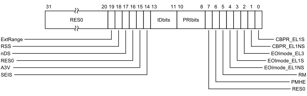
Image text
31 20 19 18 17 16 15 14 13 11 10 8 7 6 5 4 3 2 1 0
RES0 IDbits PRIbits
ExtRange CBPR_EL1S
RSS CBPR_EL1NS
nDS EOImode_EL3
RES0 EOImode_EL1S
A3V EOImode_EL1NS
SEIS RM
PMHE
RES0
ExtRange, bit [19]
Extended INTID range (read-only).
0b0 CPU interface does not support INTIDs in the range 1024..8191. Behavior is UNPREDICTABLE if the IRI delivers an interrupt in the range 1024 to 8191 to the CPU interface.
Note Arm strongly recommends that the IRI is not configured to deliver interrupts in this range to a PE that does not support them. 0b1 CPU interface supports INTIDs in the range 1024..8191
All INTIDs in the range 1024..8191 are treated as requiring deactivation.
RSS, bit [18]
Range Selector Support. Possible values are:
0b0 Targeted SGIs with affinity level 0 values of 0 - 15 are supported. 0b1 Targeted SGIs with affinity level 0 values of 0 - 255 are supported. This bit is read-only.
nDS, bit [17]
Disable Security not supported. Read-only and writes are ignored.
0b0 The CPU interface logic supports disabling of security.
0b1 The CPU interface logic does not support disabling of security, and requires that security is not disabled.
Bit [16]
Reserved, RES0.
A3V, bit [15]
Affinity 3 Valid. Read-only and writes are ignored.
0b0 The CPU interface logic does not support non-zero values of the Aff3 field in SGI generation System registers. 0b1 The CPU interface logic supports non-zero values of the Aff3 field in SGI generation System registers.
If EL3 is present, ICC_CTLR.A3V is an alias of ICC_MCTLR.A3V
SEIS, bit [14]
SEI Support. Read-only and writes are ignored. Indicates whether the CPU interface supports generation of SEIs.
0b0 The CPU interface logic does not support generation of SEIs. 0b1 The CPU interface logic supports generation of SEIs.
If EL3 is present, ICC_CTLR.SEIS is an alias of ICC_MCTLR.SEIS
IDbits, bits [13:11]
Identifier bits. Read-only and writes are ignored. Indicates the number of physical interrupt identifier bits supported.
0b000 16 bits. 0b001 24 bits.
All other values are reserved.
If EL3 is present, ICC_CTLR.IDbits is an alias of ICC_MCTLR.IDbits
PRIbits, bits [10:8]
Priority bits. Read-only and writes are ignored. The number of priority bits implemented, minus one.
An implementation that supports two Security states must implement at least 32 levels of physical priority (5 priority bits).
An implementation that supports only a single Security state must implement at least 16 levels of physical priority (4 priority bits).
Note This field always returns the number of priority bits implemented, regardless of the value of SCR.NS or the value of GICD_CTLR.DS.
The division between group priority and subpriority is defined in the binary point registers ICC_BPR0 and ICC_BPR1.
This field determines the minimum value of ICC_BPR0.
Bit [7]
Reserved, RES0.
PMHE, bit [6]
Priority Mask Hint Enable.
0b0 Disables use of the priority mask register as a hint for interrupt distribution.
0b1 Enables use of the priority mask register as a hint for interrupt distribution. Software must write ICC_PMR to 0xFF before clearing this field to 0.
An implementation might choose to make this field RAO/WI.
If EL3 is present, ICC_CTLR.PMHE is an alias of ICC_MCTLR.PMHE.
On a Warm reset, this field resets to 0.
RM, bit [5]
SBZ.
The equivalent bit in AArch64 is the Routing Modifier bit. This feature is not supported when EL3 is using AArch32.
On a Warm reset, this field resets to an architecturally UNKNOWN value.
EOImode_EL1NS, bit [4]
EOI mode for interrupts handled at Non-secure EL1 and EL2. Controls whether a write to an End of Interrupt register also deactivates the interrupt.
0b0 ICC_EOIR0 and ICC_EOIR1 provide both priority drop and interrupt deactivation functionality. Accesses to ICC_DIR are UNPREDICTABLE.
0b1 ICC_EOIR0 and ICC_EOIR1 provide priority drop functionality only. ICC_DIR provides interrupt deactivation functionality.
If EL3 is present, ICC_CTLR(NS).EOImode is an alias of ICC_MCTLR.EOImode_EL1NS.
On a Warm reset, this field resets to an architecturally UNKNOWN value.
EOImode_EL1S, bit [3]
EOI mode for interrupts handled at Secure EL1. Controls whether a write to an End of Interrupt register also deactivates the interrupt.
0b0 ICC_EOIR0 and ICC_EOIR1 provide both priority drop and interrupt deactivation functionality. Accesses to ICC_DIR are UNPREDICTABLE.
0b1 ICC_EOIR0 and ICC_EOIR1 provide priority drop functionality only. ICC_DIR provides interrupt deactivation functionality.
If EL3 is present, ICC_CTLR(S).EOImode is an alias of ICC_MCTLR.EOImode_EL1S.
On a Warm reset, this field resets to an architecturally UNKNOWN value.
EOImode_EL3, bit [2]
EOI mode for interrupts handled at EL3. Controls whether a write to an End of Interrupt register also deactivates the interrupt.
0b0 ICC_EOIR0 and ICC_EOIR1 provide both priority drop and interrupt deactivation functionality. Accesses to ICC_DIR are UNPREDICTABLE.
0b1 ICC_EOIR0 and ICC_EOIR1 provide priority drop functionality only. ICC_DIR provides interrupt deactivation functionality.
On a Warm reset, this field resets to an architecturally UNKNOWN value.
CBPR_EL1NS, bit [1]
Common Binary Point Register, EL1 Non-secure. Controls whether the same register is used for interrupt preemption of both Group 0 and Group 1 Non-secure interrupts at EL1 and EL2.
0b0 ICC_BPR0 determines the preemption group for Group 0 interrupts only. ICC_BPR1 determines the preemption group for Non-secure Group 1 interrupts. 0b1 ICC_BPR0 determines the preemption group for Group 0 interrupts and Non-secure Group 1 interrupts. Non-secure accesses to GICC_BPR and ICC_BPR1 access the state of ICC_BPR0.
If EL3 is present, ICC_CTLR(NS).CBPR is an alias of ICC_MCTLR.CBPR_EL1NS.
On a Warm reset, this field resets to an architecturally UNKNOWN value.
CBPR_EL1S, bit [0]
Common Binary Point Register, EL1 Secure. Controls whether the same register is used for interrupt preemption of both Group 0 and Group 1 Secure interrupts in Secure non-Monitor modes.
0b0 ICC_BPR0 determines the preemption group for Group 0 interrupts only. ICC_BPR1 determines the preemption group for Secure Group 1 interrupts.
0b1 ICC_BPR0 determines the preemption group for Group 0 interrupts and Secure Group 1 interrupts. Secure EL1 accesses, or EL3 accesses when not in Monitor mode, to ICC_BPR1 access the state of ICC_BPR0.
If EL3 is present, ICC_CTLR(S).CBPR is an alias of ICC_MCTLR.CBPR_EL1S. On a Warm reset, this field resets to an architecturally UNKNOWN value.
Accessing the ICC_MCTLR
This register is only accessible when executing in Monitor mode.
Accesses to this register use the following encodings in the System instruction encoding space:
MRC{}{} , {#},
}, {#} ,
| coproc | opc1 | CRn | CRm | opc2 |
|---|---|---|---|---|
| 0b1111 | 0b110 | 0b1100 | 0b1100 | 0b100 |
if PSTATE.EL == EL0 then UNDEFINED;
elsif PSTATE.EL == EL1 then
if EL2Enabled() && !ELUsingAArch32(EL2) && HSTR_EL2.T12 == '1' then AArch64.AArch32SystemAccessTrap(EL2, 0x03);
elsif EL2Enabled() && ELUsingAArch32(EL2) && HSTR.T12 == '1' then AArch32.TakeHypTrapException(0x03);
else UNDEFINED;
elsif PSTATE.EL == EL2 then UNDEFINED;
elsif PSTATE.EL == EL3 then
if ICC_MSRE.SRE == '0' then UNDEFINED;
else return ICC_MCTLR;
MCR{}{} , {#},
}, {#} ,
| coproc | opc1 | CRn | CRm | opc2 |
|---|---|---|---|---|
| 0b1111 | 0b110 | 0b1100 | 0b1100 | 0b100 |
if PSTATE.EL == EL0 then UNDEFINED;
elsif PSTATE.EL == EL1 then
if EL2Enabled() && !ELUsingAArch32(EL2) && HSTR_EL2.T12 == '1' then AArch64.AArch32SystemAccessTrap(EL2, 0x03);
elsif EL2Enabled() && ELUsingAArch32(EL2) && HSTR.T12 == '1' then AArch32.TakeHypTrapException(0x03);
else UNDEFINED;
elsif PSTATE.EL == EL2 then UNDEFINED;
elsif PSTATE.EL == EL3 then
if ICC_MSRE.SRE == '0' then UNDEFINED;
else ICC_MCTLR = R[t];
12.5.18 ICC_MGRPEN1, Interrupt Controller Monitor Interrupt Group 1 Enable register
The ICC_MGRPEN1 characteristics are:
Purpose
Controls whether Group 1 interrupts are enabled or not.
Configurations
AArch32 System register ICC_MGRPEN1 bits [31:0] can be mapped to AArch64 System register ICC_IGRPEN1_EL3[31:0], but this is not architecturally mandated.
This register is present only when AArch32 is supported at any Exception level. Otherwise, direct accesses to ICC_MGRPEN1 are UNDEFINED.
Attributes
ICC_MGRPEN1 is a 32-bit register.
Field descriptions
The ICC_MGRPEN1 bit assignments are:
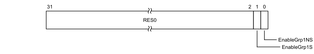
31 2 1 0
RES0
EnableGrp1NS
EnableGrp1S
Bits [31:2]
Reserved, RES0.
EnableGrp1S, bit [1]
Enables Group 1 interrupts for the Secure state.
0b0 Secure Group 1 interrupts are disabled.
0b1 Secure Group 1 interrupts are enabled.
The Secure ICC_IGRPEN1.Enable bit is a read/write alias of the ICC_MGRPEN1.EnableGrp1S bit.
If the highest priority pending interrupt for that PE is a Group 1 interrupt using 1 of N model, then the interrupt will target another PE as a result of the Enable bit changing from 1 to 0.
On a Warm reset, this field resets to 0.
EnableGrp1NS, bit [0]
Enables Group 1 interrupts for the Non-secure state.
0b0 Non-secure Group 1 interrupts are disabled.
0b1 Non-secure Group 1 interrupts are enabled.
The Non-secure ICC_IGRPEN1.Enable bit is a read/write alias of the ICC_MGRPEN1.EnableGrp1NS bit.
If the highest priority pending interrupt for that PE is a Group 1 interrupt using 1 of N model, then the interrupt will target another PE as a result of the Enable bit changing from 1 to 0. On a Warm reset, this field resets to 0.
Accessing the ICC_MGRPEN1
If an interrupt is pending within the CPU interface when an Enable bit becomes 0, the interrupt must be released to allow the Distributor to forward the interrupt to a different PE.
This register is only accessible when executing in Monitor mode.
Accesses to this register use the following encodings in the System instruction encoding space:
MRC{}{} , {#},
}, {#} ,
| coproc | opc1 | CRn | CRm | opc2 |
|---|---|---|---|---|
| 0b1111 | 0b110 | 0b1100 | 0b1100 | 0b111 |
if PSTATE.EL == EL0 then UNDEFINED;
elsif PSTATE.EL == EL1 then
if EL2Enabled() && !ELUsingAArch32(EL2) && HSTR_EL2.T12 == '1' then AArch64.AArch32SystemAccessTrap(EL2, 0x03);
elsif EL2Enabled() && ELUsingAArch32(EL2) && HSTR.T12 == '1' then AArch32.TakeHypTrapException(0x03);
else UNDEFINED;
elsif PSTATE.EL == EL2 then UNDEFINED;
elsif PSTATE.EL == EL3 then
if ICC_MSRE.SRE == '0' then UNDEFINED;
else return ICC_MGRPEN1;
MCR{}{} , {#},
}, {#} ,
| coproc | opc1 | CRn | CRm | opc2 |
|---|---|---|---|---|
| 0b1111 | 0b110 | 0b1100 | 0b1100 | 0b111 |
if PSTATE.EL == EL0 then UNDEFINED;
elsif PSTATE.EL == EL1 then
if EL2Enabled() && !ELUsingAArch32(EL2) && HSTR_EL2.T12 == '1' then AArch64.AArch32SystemAccessTrap(EL2, 0x03);
elsif EL2Enabled() && ELUsingAArch32(EL2) && HSTR.T12 == '1' then AArch32.TakeHypTrapException(0x03);
else UNDEFINED;
elsif PSTATE.EL == EL2 then UNDEFINED;
elsif PSTATE.EL == EL3 then
if ICC_MSRE.SRE == '0' then UNDEFINED;
else ICC_MGRPEN1 = R[t];
12.5.19 ICC_MSRE, Interrupt Controller Monitor System Register Enable register
The ICC_MSRE characteristics are:
Purpose
Controls whether the System register interface or the memory-mapped interface to the GIC CPU interface is used for EL3.
Configurations
AArch32 System register ICC_MSRE bits [31:0] can be mapped to AArch64 System register ICC_SRE_EL3[31:0], but this is not architecturally mandated.
This register is present only when AArch32 is supported at any Exception level. Otherwise, direct accesses to ICC_MSRE are UNDEFINED.
Attributes
ICC_MSRE is a 32-bit register.
Field descriptions
The ICC_MSRE bit assignments are:

Image text
31 4 3 2 1 0
RES0
SRE
DFB
DIB
Enable
Enable, bit [3]
Enable. Enables lower Exception level access to ICC_SRE and ICC_HSRE.
0b0 Secure EL1 accesses to Secure ICC_SRE trap to EL3. EL2 accesses to Non-secure ICC_SRE and ICC_HSRE trap to EL3. Non-secure EL1 accesses to ICC_SRE trap to EL3, unless these accesses are trapped to EL2 as a result of ICC_HSRE.Enable == 0. 0b1 Secure EL1 accesses to Secure ICC_SRE do not trap to EL3. EL2 accesses to Non-secure ICC_SRE and ICC_HSRE do not trap to EL3. Non-secure EL1 accesses to ICC_SRE do not trap to EL3.
If ICC_MSRE.SRE is RAO/WI, an implementation is permitted to make the Enable bit RAO/WI.
If ICC_MSRE.SRE is 0, the Enable bit behaves as 1 for all purposes other than reading the value of the bit.
On a Warm reset, this field resets to an architecturally UNKNOWN value.
DIB, bit [2]
Disable IRQ bypass. 0b0 IRQ bypass enabled. 0b1 IRQ bypass disabled.
In systems that do not support IRQ bypass, this bit is RAO/WI. On a Warm reset, this field resets to 0.
DFB, bit [1]
Disable FIQ bypass.
0b0 FIQ bypass enabled. 0b1 FIQ bypass disabled.
In systems that do not support FIQ bypass, this bit is RAO/WI.
On a Warm reset, this field resets to 0.
SRE, bit [0]
System Register Enable.
0b0 The memory-mapped interface must be used. Accesses at EL3 or below to any ICH_* System register, or any EL1, EL2, or EL3 ICC_* register other than ICC_SRE, ICC_HSRE, or ICC_MSRE, are UNDEFINED.
0b1 The System register interface to the ICH_* registers and the EL1, EL2, and EL3 ICC_* registers is enabled for EL3.
If software changes this bit from 1 to 0, the results are UNPREDICTABLE.
If an implementation supports only a System register interface to the GIC CPU interface, this bit is RAO/WI.
On a Warm reset, this field resets to 0.
Accessing the ICC_MSRE
This register is always System register accessible.
The GIC architecture permits, but does not require, that registers can be shared between memory-mapped registers and the equivalent System registers. This means that if the memory-mapped registers have been accessed while ICC_MSRE.SRE==0, then the System registers might be modified. Therefore, software must only rely on the reset values of the System registers if there has been no use of the GIC functionality while the memory-mapped registers are in use. Otherwise, the System register values must be treated as UNKNOWN.
This register is only accessible when executing in Monitor mode.
Accesses to this register use the following encodings in the System instruction encoding space:
MRC{}{} , {#},
}, {#} ,
| coproc | opc1 | CRn | CRm | opc2 |
|---|---|---|---|---|
| 0b1111 | 0b110 | 0b1100 | 0b1100 | 0b101 |
if PSTATE.EL == EL0 then UNDEFINED;
elsif PSTATE.EL == EL1 then
if EL2Enabled() && !ELUsingAArch32(EL2) && HSTR_EL2.T12 == '1' then AArch64.AArch32SystemAccessTrap(EL2, 0x03);
elsif EL2Enabled() && ELUsingAArch32(EL2) && HSTR.T12 == '1' then AArch32.TakeHypTrapException(0x03);
else UNDEFINED;
elsif PSTATE.EL == EL2 then UNDEFINED;
elsif PSTATE.EL == EL3 then
return ICC_MSRE;
MCR{}{} , {#},
}, {#} ,
| coproc | opc1 | CRn | CRm | opc2 |
|---|---|---|---|---|
| 0b1111 | 0b110 | 0b1100 | 0b1100 | 0b101 |
if PSTATE.EL == EL0 then UNDEFINED;
elsif PSTATE.EL == EL1 then
if EL2Enabled() && !ELUsingAArch32(EL2) && HSTR_EL2.T12 == '1' then AArch64.AArch32SystemAccessTrap(EL2, 0x03);
elsif EL2Enabled() && ELUsingAArch32(EL2) && HSTR.T12 == '1' then AArch32.TakeHypTrapException(0x03);
else UNDEFINED;
elsif PSTATE.EL == EL2 then UNDEFINED;
elsif PSTATE.EL == EL3 then
if SCR.NS == '0' && CP15SDISABLE2 == HIGH then UNDEFINED;
else ICC_MSRE = R[t];
12.5.20 ICC_PMR, Interrupt Controller Interrupt Priority Mask Register
The ICC_PMR characteristics are:
Purpose
Provides an interrupt priority filter. Only interrupts with a higher priority than the value in this register are signaled to the PE.
Configurations
AArch32 System register ICC_PMR bits [31:0] are architecturally mapped to AArch64 System register ICC_PMR_EL1[31:0].
This register is present only when AArch32 is supported at any Exception level. Otherwise, direct accesses to ICC_PMR are UNDEFINED.
To allow software to ensure appropriate observability of actions initiated by GIC register accesses, the PE and CPU interface logic must ensure that writes to this register are self-synchronising. This ensures that no interrupts below the written PMR value will be taken after a write to this register is architecturally executed. For more information, see Observability of the effects of accesses to the GIC registers.
Attributes
ICC_PMR is a 32-bit register.
Field descriptions
The ICC_PMR bit assignments are:

31 8 7 0
RES0 Priority
Bits [31:8]
Reserved, RES0.
Priority, bits [7:0]
The priority mask level for the CPU interface. If the priority of an interrupt is higher than the value indicated by this field, the interface signals the interrupt to the PE.
The possible priority field values are as follows:
| Implemented priority bits | Possible priority field values | Number of priority levels |
|---|---|---|
| [7:0] | 0x00-0xFF(0-255), all values | 256 |
| [7:1] | 0x00-0xFE(0-254), even values only | 128 |
| [7:2] | 0x00-0xFC(0-252), in steps of 4 | 64 |
| [7:3] | 0x00-0xF8(0-248), in steps of 8 | 32 |
| [7:4] | 0x00-0xF0(0-240), in steps of 16 | 16 |
Unimplemented priority bits are RAZ/WI.
On a Warm reset, this field resets to 0.
Accessing the ICC_PMR
Accesses to this register use the following encodings in the System instruction encoding space:
MRC{}{} , {#},
}, {#} ,
| coproc | opc1 | CRn | CRm | opc2 |
|---|---|---|---|---|
| 0b1111 | 0b000 | 0b0100 | 0b0110 | 0b000 |
if PSTATE.EL == EL0 then UNDEFINED;
elsif PSTATE.EL == EL1 then
if Halted() && HaveEL(EL3) && EDSCR.SDD == '1' &&
boolean IMPLEMENTATION_DEFINED "EL3 trap priority
when SDD == '1'" && !ELUsingAArch32(EL3) && SCR_EL3.<IRQ,FIQ> == '11' then UNDEFINED;
elsif Halted() && HaveEL(EL3) && EDSCR.SDD == '1' &&
boolean IMPLEMENTATION_DEFINED "EL3 trap priority
when SDD == '1'" && ELUsingAArch32(EL3) && PSTATE.M != M32_Monitor && SCR.<IRQ,FIQ> == '11' then UNDEFINED;
elsif EL2Enabled() && !ELUsingAArch32(EL2) && HSTR_EL2.T12 == '1' then AArch64.AArch32SystemAccessTrap(EL2, 0x03);
elsif EL2Enabled() && ELUsingAArch32(EL2) && HSTR.T12 == '1' then AArch32.TakeHypTrapException(0x03);
elsif EL2Enabled() && !ELUsingAArch32(EL2) && ICH_HCR_EL2.TC == '1' then AArch64.AArch32SystemAccessTrap(EL2, 0x03);
elsif EL2Enabled() && ELUsingAArch32(EL2) && ICH_HCR.TC == '1' then AArch32.TakeHypTrapException(0x03);
elsif EL2Enabled() && !ELUsingAArch32(EL2) && HCR_EL2.FMO == '1' then
return ICV_PMR;
elsif EL2Enabled() && !ELUsingAArch32(EL2) && HCR_EL2.IMO == '1' then
return ICV_PMR;
elsif EL2Enabled() && ELUsingAArch32(EL2) && HCR.FMO == '1' then
return ICV_PMR;
elsif EL2Enabled() && ELUsingAArch32(EL2) && HCR.IMO == '1' then
return ICV_PMR;
elsif HaveEL(EL3) && !ELUsingAArch32(EL3) && SCR_EL3.<IRQ,FIQ> == '11' then
if Halted() && EDSCR.SDD == '1' then UNDEFINED;
else AArch64.AArch32SystemAccessTrap(EL3, 0x03);
elsif HaveEL(EL3) && ELUsingAArch32(EL3) && PSTATE.M != M32_Monitor && SCR.<IRQ,FIQ> == '11' then
if Halted() && EDSCR.SDD == '1' then UNDEFINED;
else AArch32.TakeMonitorTrapException();
else return ICC_PMR;
elsif PSTATE.EL == EL2 then
if Halted() && HaveEL(EL3) && EDSCR.SDD == '1' &&
boolean IMPLEMENTATION_DEFINED "EL3 trap priority
when SDD == '1'" && !ELUsingAArch32(EL3) && SCR_EL3.<IRQ,FIQ> == '11' then UNDEFINED;
elsif Halted() && HaveEL(EL3) && EDSCR.SDD == '1' &&
boolean IMPLEMENTATION_DEFINED "EL3 trap priority
when SDD == '1'" && ELUsingAArch32(EL3) && SCR.<IRQ,FIQ> == '11' then UNDEFINED;
elsif ICC_HSRE.SRE == '0' then UNDEFINED;
elsif HaveEL(EL3) && !ELUsingAArch32(EL3) && SCR_EL3.<IRQ,FIQ> == '11' then
if Halted() && EDSCR.SDD == '1' then UNDEFINED;
else AArch64.AArch32SystemAccessTrap(EL3, 0x03);
elsif HaveEL(EL3) && ELUsingAArch32(EL3) && SCR.<IRQ,FIQ> == '11' then
if Halted() && EDSCR.SDD == '1' then UNDEFINED;
else AArch32.TakeMonitorTrapException();
else return ICC_PMR;
elsif PSTATE.EL == EL3 then
if ICC_MSRE.SRE == '0' then UNDEFINED;
else return ICC_PMR;
MCR{}{} , {#},
}, {#} ,
| coproc | opc1 | CRn | CRm | opc2 |
|---|---|---|---|---|
| 0b1111 | 0b000 | 0b0100 | 0b0110 | 0b000 |
if PSTATE.EL == EL0 then UNDEFINED;
elsif PSTATE.EL == EL1 then
if Halted() && HaveEL(EL3) && EDSCR.SDD == '1' &&
boolean IMPLEMENTATION_DEFINED "EL3 trap priority
when SDD == '1'" && !ELUsingAArch32(EL3) && SCR_EL3.<IRQ,FIQ> == '11' then UNDEFINED;
elsif Halted() && HaveEL(EL3) && EDSCR.SDD == '1' &&
boolean IMPLEMENTATION_DEFINED "EL3 trap priority
when SDD == '1'" && ELUsingAArch32(EL3) && PSTATE.M != M32_Monitor && SCR.<IRQ,FIQ> == '11' then UNDEFINED;
elsif EL2Enabled() && !ELUsingAArch32(EL2) && HSTR_EL2.T12 == '1' then AArch64.AArch32SystemAccessTrap(EL2, 0x03);
elsif EL2Enabled() && ELUsingAArch32(EL2) && HSTR.T12 == '1' then AArch32.TakeHypTrapException(0x03);
elsif EL2Enabled() && !ELUsingAArch32(EL2) && ICH_HCR_EL2.TC == '1' then AArch64.AArch32SystemAccessTrap(EL2, 0x03);
elsif EL2Enabled() && ELUsingAArch32(EL2) && ICH_HCR.TC == '1' then AArch32.TakeHypTrapException(0x03);
elsif EL2Enabled() && !ELUsingAArch32(EL2) && HCR_EL2.FMO == '1' then ICV_PMR = R[t];
elsif EL2Enabled() && !ELUsingAArch32(EL2) && HCR_EL2.IMO == '1' then ICV_PMR = R[t];
elsif EL2Enabled() && ELUsingAArch32(EL2) && HCR.FMO == '1' then ICV_PMR = R[t];
elsif EL2Enabled() && ELUsingAArch32(EL2) && HCR.IMO == '1' then ICV_PMR = R[t];
elsif HaveEL(EL3) && !ELUsingAArch32(EL3) && SCR_EL3.<IRQ,FIQ> == '11' then
if Halted() && EDSCR.SDD == '1' then UNDEFINED;
else AArch64.AArch32SystemAccessTrap(EL3, 0x03);
elsif HaveEL(EL3) && ELUsingAArch32(EL3) && PSTATE.M != M32_Monitor && SCR.<IRQ,FIQ> == '11' then
if Halted() && EDSCR.SDD == '1' then UNDEFINED;
else AArch32.TakeMonitorTrapException();
else ICC_PMR = R[t];
elsif PSTATE.EL == EL2 then
if Halted() && HaveEL(EL3) && EDSCR.SDD == '1' &&
boolean IMPLEMENTATION_DEFINED "EL3 trap priority
when SDD == '1'" && !ELUsingAArch32(EL3) && SCR_EL3.<IRQ,FIQ> == '11' then UNDEFINED;
elsif Halted() && HaveEL(EL3) && EDSCR.SDD == '1' &&
boolean IMPLEMENTATION_DEFINED "EL3 trap priority
when SDD == '1'" && ELUsingAArch32(EL3) && SCR.<IRQ,FIQ> == '11' then UNDEFINED;
elsif ICC_HSRE.SRE == '0' then UNDEFINED;
elsif HaveEL(EL3) && !ELUsingAArch32(EL3) && SCR_EL3.<IRQ,FIQ> == '11' then
if Halted() && EDSCR.SDD == '1' then UNDEFINED;
else AArch64.AArch32SystemAccessTrap(EL3, 0x03);
elsif HaveEL(EL3) && ELUsingAArch32(EL3) && SCR.<IRQ,FIQ> == '11' then
if Halted() && EDSCR.SDD == '1' then UNDEFINED;
else AArch32.TakeMonitorTrapException();
else ICC_PMR = R[t];
elsif PSTATE.EL == EL3 then
if ICC_MSRE.SRE == '0' then UNDEFINED;
else ICC_PMR = R[t];
12.5.21 ICC_RPR, Interrupt Controller Running Priority Register
The ICC_RPR characteristics are:
Purpose
Indicates the Running priority of the CPU interface.
Configurations
AArch32 System register ICC_RPR performs the same function as AArch64 System register ICC_RPR_EL1.
This register is present only when AArch32 is supported at any Exception level. Otherwise, direct accesses to ICC_RPR are UNDEFINED.
Attributes
ICC_RPR is a 32-bit register.
Field descriptions
The ICC_RPR bit assignments are:

31 8 7 0
RES0 Priority
Bits [31:8]
Reserved, RES0.
Priority, bits [7:0]
The current running priority on the CPU interface. This is the group priority of the current active interrupt.
The priority returned is the group priority as if the BPR for the current Exception level and Security state was set to the minimum value of BPR for the number of implemented priority bits.

Note If 8 bits of priority are implemented the group priority is bits[7:1] of the priority.
Accessing the ICC_RPR
If there are no active interrupts on the CPU interface, or all active interrupts have undergone a priority drop, the value returned is the Idle priority.
Software cannot determine the number of implemented priority bits from a read of this register.
Accesses to this register use the following encodings in the System instruction encoding space:
MRC{}{} , {#},
}, {#} ,
| coproc | opc1 | CRn | CRm | opc2 |
|---|---|---|---|---|
| 0b1111 | 0b000 | 0b1100 | 0b1011 | 0b011 |
if PSTATE.EL == EL0 then UNDEFINED;
elsif PSTATE.EL == EL1 then
if Halted() && HaveEL(EL3) && EDSCR.SDD == '1' &&
boolean IMPLEMENTATION_DEFINED "EL3 trap priority
when SDD == '1'" && !ELUsingAArch32(EL3) && SCR_EL3.<IRQ,FIQ> == '11' then UNDEFINED;
elsif Halted() && HaveEL(EL3) && EDSCR.SDD == '1' &&
boolean IMPLEMENTATION_DEFINED "EL3 trap priority
when SDD == '1'" && ELUsingAArch32(EL3) && PSTATE.M != M32_Monitor && SCR.<IRQ,FIQ> == '11' then UNDEFINED;
elsif EL2Enabled() && !ELUsingAArch32(EL2) && HSTR_EL2.T12 == '1' then AArch64.AArch32SystemAccessTrap(EL2, 0x03);
elsif EL2Enabled() && ELUsingAArch32(EL2) && HSTR.T12 == '1' then AArch32.TakeHypTrapException(0x03);
elsif EL2Enabled() && !ELUsingAArch32(EL2) && ICH_HCR_EL2.TC == '1' then AArch64.AArch32SystemAccessTrap(EL2, 0x03);
elsif EL2Enabled() && ELUsingAArch32(EL2) && ICH_HCR.TC == '1' then AArch32.TakeHypTrapException(0x03);
elsif EL2Enabled() && !ELUsingAArch32(EL2) && HCR_EL2.FMO == '1' then
return ICV_RPR;
elsif EL2Enabled() && !ELUsingAArch32(EL2) && HCR_EL2.IMO == '1' then
return ICV_RPR;
elsif EL2Enabled() && ELUsingAArch32(EL2) && HCR.FMO == '1' then
return ICV_RPR;
elsif EL2Enabled() && ELUsingAArch32(EL2) && HCR.IMO == '1' then
return ICV_RPR;
elsif HaveEL(EL3) && !ELUsingAArch32(EL3) && SCR_EL3.<IRQ,FIQ> == '11' then
if Halted() && EDSCR.SDD == '1' then UNDEFINED;
else AArch64.AArch32SystemAccessTrap(EL3, 0x03);
elsif HaveEL(EL3) && ELUsingAArch32(EL3) && PSTATE.M != M32_Monitor && SCR.<IRQ,FIQ> == '11' then
if Halted() && EDSCR.SDD == '1' then UNDEFINED;
else AArch32.TakeMonitorTrapException();
else return ICC_RPR;
elsif PSTATE.EL == EL2 then
if Halted() && HaveEL(EL3) && EDSCR.SDD == '1' &&
boolean IMPLEMENTATION_DEFINED "EL3 trap priority
when SDD == '1'" && !ELUsingAArch32(EL3) && SCR_EL3.<IRQ,FIQ> == '11' then UNDEFINED;
elsif Halted() && HaveEL(EL3) && EDSCR.SDD == '1' &&
boolean IMPLEMENTATION_DEFINED "EL3 trap priority
when SDD == '1'" && ELUsingAArch32(EL3) && SCR.<IRQ,FIQ> == '11' then UNDEFINED;
elsif ICC_HSRE.SRE == '0' then UNDEFINED;
elsif HaveEL(EL3) && !ELUsingAArch32(EL3) && SCR_EL3.<IRQ,FIQ> == '11' then
if Halted() && EDSCR.SDD == '1' then UNDEFINED;
else AArch64.AArch32SystemAccessTrap(EL3, 0x03);
elsif HaveEL(EL3) && ELUsingAArch32(EL3) && SCR.<IRQ,FIQ> == '11' then
if Halted() && EDSCR.SDD == '1' then UNDEFINED;
else AArch32.TakeMonitorTrapException();
else return ICC_RPR;
elsif PSTATE.EL == EL3 then
if ICC_MSRE.SRE == '0' then UNDEFINED;
else return ICC_RPR;
12.5.22 ICC_SGI0R, Interrupt Controller Software Generated Interrupt Group 0 Register
The ICC_SGI0R characteristics are:
Purpose
Generates Secure Group 0 SGIs.
Configurations
AArch32 System register ICC_SGI0R performs the same function as AArch64 System register ICC_SGI0R_EL1.
This register is present only when AArch32 is supported at any Exception level. Otherwise, direct accesses to ICC_SGI0R are UNDEFINED.
Attributes
ICC_SGI0R is a 64-bit register.
Field descriptions
The ICC_SGI0R bit assignments are:
IRM

63 56 55 48 47 44 43 41 40 39 32 31 28 27 24 23 16 15 0
RES0 Aff3 RS RES0 Aff2 RES0 INTID Aff1 TargetList
Bits [63:56]
Reserved, RES0.
Aff3, bits [55:48]
The affinity 3 value of the affinity path of the cluster for which SGI interrupts will be generated. If the IRM bit is 1, this field is RES0.
RS, bits [47:44]
RangeSelector Controls which group of 16 values is represented by the TargetList field. TargetList[n] represents aff0 value ((RS * 16) + n). When ICC_CTLR_EL1.RSS==0, RS is RES0. When ICC_CTLR_EL1.RSS==1 and GICD_TYPER.RSS==0, writing this register with RS != 0 is a CONSTRAINED UNPREDICTABLE choice of : • The write is ignored. • The RS field is treated as 0.
Bits [43:41]
Reserved, RES0.
IRM, bit [40]
Interrupt Routing Mode. Determines how the generated interrupts are distributed to PEs. Possible values are: 0b0 Interrupts routed to the PEs specified by Aff3.Aff2.Aff1.
Aff2, bits [39:32]
The affinity 2 value of the affinity path of the cluster for which SGI interrupts will be generated. If the IRM bit is 1, this field is RES0.
Bits [31:28]
Reserved, RES0.
INTID, bits [27:24]
The INTID of the SGI.
Aff1, bits [23:16]
The affinity 1 value of the affinity path of the cluster for which SGI interrupts will be generated.
If the IRM bit is 1, this field is RES0.
TargetList, bits [15:0]
Target List. The set of PEs for which SGI interrupts will be generated. Each bit corresponds to the PE within a cluster with an Affinity 0 value equal to the bit number.
If a bit is 1 and the bit does not correspond to a valid target PE, the bit must be ignored by the Distributor. It is IMPLEMENTATION DEFINED whether, in such cases, a Distributor can signal a system error.
Note This restricts a system to sending targeted SGIs to PEs with an affinity 0 number that is less than 16. If SRE is set only for Secure EL3, software executing at EL3 might use the System register interface to generate SGIs. Therefore, the Distributor must always be able to receive and acknowledge Generate SGI packets received from CPU interface regardless of the ARE settings for a Security state. However, the Distributor might discard such packets.
If the IRM bit is 1, this field is RES0.
Accessing the ICC_SGI0R
This register allows software executing in a Secure state to generate Group 0 SGIs. It will also allow software executing in a Non-secure state to generate Group 0 SGIs, if permitted by the settings of GICR_NSACR in the Redistributor corresponding to the target PE.
When GICD_CTLR.DS==0, Non-secure writes do not generate an interrupt for a target PE if not permitted by the GICR_NSACR register associated with the target PE. For more information, see Use of control registers for SGI forwarding.
Note Accesses from Secure Monitor mode are treated as Secure regardless of the value of SCR.NS.
Accesses to this register use the following encodings in the System instruction encoding space:
MCRR{}{} , {#},
}, {#} ,
| coproc | CRm | opc1 |
|---|---|---|
| 0b1111 | 0b1100 | 0b0010 |
if PSTATE.EL == EL0 then UNDEFINED;
elsif PSTATE.EL == EL1 then
if Halted() && HaveEL(EL3) && EDSCR.SDD == '1' &&
boolean IMPLEMENTATION_DEFINED "EL3 trap priority
when SDD == '1'" && !ELUsingAArch32(EL3) && SCR_EL3.<IRQ,FIQ> == '11' then
UNDEFINED;
elsif Halted() && HaveEL(EL3) && EDSCR.SDD == '1' &&
boolean IMPLEMENTATION_DEFINED "EL3 trap priority when SDD == '1'" && ELUsingAArch32(EL3) && PSTATE.M != M32_Monitor && SCR.<IRQ,FIQ> == '11'
then UNDEFINED;
elsif EL2Enabled() && !ELUsingAArch32(EL2) && HSTR_EL2.T12 == '1'
then AArch64.AArch32SystemAccessTrap(EL2, 0x03);
elsif EL2Enabled() && ELUsingAArch32(EL2) && HSTR.T12 == '1'
then AArch32.TakeHypTrapException(0x03);
elsif ICC_SRE.SRE == '0'
then UNDEFINED;
elsif EL2Enabled() && !ELUsingAArch32(EL2) && ICH_HCR_EL2.TC == '1'
then AArch64.AArch32SystemAccessTrap(EL2, 0x03);
elsif EL2Enabled() && ELUsingAArch32(EL2) && ICH_HCR.TC == '1'
then AArch32.TakeHypTrapException(0x03);
elsif EL2Enabled() && !ELUsingAArch32(EL2) && HCR_EL2.FMO == '1'
then AArch64.AArch32SystemAccessTrap(EL2, 0x03);
elsif EL2Enabled() && !ELUsingAArch32(EL2) && HCR_EL2.IMO == '1'
then AArch64.AArch32SystemAccessTrap(EL2, 0x03);
elsif EL2Enabled() && ELUsingAArch32(EL2) && HCR.FMO == '1'
then AArch32.TakeHypTrapException(0x03);
elsif EL2Enabled() && ELUsingAArch32(EL2) && HCR.IMO == '1'
then AArch32.TakeHypTrapException(0x03);
elsif HaveEL(EL3) && !ELUsingAArch32(EL3) && SCR_EL3.<IRQ,FIQ> == '11'
then if Halted() && EDSCR.SDD == '1'
then UNDEFINED;
else AArch64.AArch32SystemAccessTrap(EL3, 0x03);
elsif HaveEL(EL3) && ELUsingAArch32(EL3) && PSTATE.M != M32_Monitor && SCR.<IRQ,FIQ> == '11'
then if Halted() && EDSCR.SDD == '1'
then UNDEFINED;
else AArch32.TakeMonitorTrapException();
else ICC_SGI0R = R[t2]:R[t];
elsif PSTATE.EL == EL2
then
if Halted() && HaveEL(EL3) && EDSCR.SDD == '1' &&
boolean IMPLEMENTATION_DEFINED "EL3 trap priority when SDD == '1'" && !ELUsingAArch32(EL3) && SCR_EL3.<IRQ,FIQ> == '11'
then UNDEFINED;
elsif Halted() && HaveEL(EL3) && EDSCR.SDD == '1' &&
boolean IMPLEMENTATION_DEFINED "EL3 trap priority when SDD == '1'" && ELUsingAArch32(EL3) && SCR.<IRQ,FIQ> == '11'
then UNDEFINED;
elsif ICC_HSRE.SRE == '0'
then UNDEFINED;
elsif HaveEL(EL3) && !ELUsingAArch32(EL3) && SCR_EL3.<IRQ,FIQ> == '11'
then if Halted() && EDSCR.SDD == '1'
then UNDEFINED;
else AArch64.AArch32SystemAccessTrap(EL3, 0x03);
elsif HaveEL(EL3) && ELUsingAArch32(EL3) && SCR.<IRQ,FIQ> == '11'
then if Halted() && EDSCR.SDD == '1'
then UNDEFINED;
else AArch32.TakeMonitorTrapException();
else ICC_SGI0R = R[t2]:R[t];
elsif PSTATE.EL == EL3
then if ICC_MSRE.SRE == '0'
then UNDEFINED;
else ICC_SGI0R = R[t2]:R[t];
12.5.23 ICC_SGI1R, Interrupt Controller Software Generated Interrupt Group 1 Register
The ICC_SGI1R characteristics are:
Purpose
Generates Group 1 SGIs for the current Security state.
Configurations
AArch32 System register ICC_SGI1R performs the same function as AArch64 System register ICC_SGI1R_EL1.
This register is present only when AArch32 is supported at any Exception level. Otherwise, direct accesses to ICC_SGI1R are UNDEFINED.
Under certain conditions a write to ICC_SGI1R can generate Group 0 interrupts, see Table 12-14.
Attributes
ICC_SGI1R is a 64-bit register.
Field descriptions
The ICC_SGI1R bit assignments are:
IRM
| 63 56 55 48 47 44 43 41 40 39 32 31 28 27 24 23 16 15 0 | 63 56 55 48 47 44 43 41 40 39 32 31 28 27 24 23 16 15 0 | 63 56 55 48 47 44 43 41 40 39 32 31 28 27 24 23 16 15 0 | 63 56 55 48 47 44 43 41 40 39 32 31 28 27 24 23 16 15 0 | 63 56 55 48 47 44 43 41 40 39 32 31 28 27 24 23 16 15 0 | 63 56 55 48 47 44 43 41 40 39 32 31 28 27 24 23 16 15 0 | 63 56 55 48 47 44 43 41 40 39 32 31 28 27 24 23 16 15 0 | 63 56 55 48 47 44 43 41 40 39 32 31 28 27 24 23 16 15 0 | 63 56 55 48 47 44 43 41 40 39 32 31 28 27 24 23 16 15 0 | 63 56 55 48 47 44 43 41 40 39 32 31 28 27 24 23 16 15 0 | 63 56 55 48 47 44 43 41 40 39 32 31 28 27 24 23 16 15 0 | 63 56 55 48 47 44 43 41 40 39 32 31 28 27 24 23 16 15 0 |
|---|---|---|---|---|---|---|---|---|---|---|---|
| RES0 Aff3 RS RES0 Aff2 RES0 INTID Aff1 TargetList | RES0 | Aff3 | RS | RES0 | Aff2 | RES0 | INTID | Aff1 | TargetList | ||
Bits [63:56]
Reserved, RES0.
Aff3, bits [55:48]
The affinity 3 value of the affinity path of the cluster for which SGI interrupts will be generated. If the IRM bit is 1, this field is RES0.
RS, bits [47:44]
RangeSelector
Controls which group of 16 values is represented by the TargetList field.
TargetList[n] represents aff0 value ((RS * 16) + n).
When ICC_CTLR_EL1.RSS==0, RS is RES0.
When ICC_CTLR_EL1.RSS==1 and GICD_TYPER.RSS==0, writing this register with RS != 0 is a CONSTRAINED UNPREDICTABLE choice of :
• The write is ignored. • The RS field is treated as 0.
Bits [43:41]
Reserved, RES0.
IRM, bit [40]
Interrupt Routing Mode. Determines how the generated interrupts are distributed to PEs. Possible values are: 0b0 Interrupts routed to the PEs specified by Aff3.Aff2.Aff1.
Aff2, bits [39:32]
The affinity 2 value of the affinity path of the cluster for which SGI interrupts will be generated. If the IRM bit is 1, this field is RES0.
Bits [31:28]
Reserved, RES0.
INTID, bits [27:24]
The INTID of the SGI.
Aff1, bits [23:16]
The affinity 1 value of the affinity path of the cluster for which SGI interrupts will be generated. If the IRM bit is 1, this field is RES0.
TargetList, bits [15:0]
Target List. The set of PEs for which SGI interrupts will be generated. Each bit corresponds to the PE within a cluster with an Affinity 0 value equal to the bit number.
If a bit is 1 and the bit does not correspond to a valid target PE, the bit must be ignored by the Distributor. It is IMPLEMENTATION DEFINED whether, in such cases, a Distributor can signal a system error.
Note
This restricts a system to sending targeted SGIs to PEs with an affinity 0 number that is less than 16. If SRE is set only for Secure EL3, software executing at EL3 might use the System register interface to generate SGIs. Therefore, the Distributor must always be able to receive and acknowledge Generate SGI packets received from CPU interface regardless of the ARE settings for a Security state. However, the Distributor might discard such packets.
If the IRM bit is 1, this field is RES0.
Accessing the ICC_SGI1R
Note Accesses from Secure Monitor mode are treated as Secure regardless of the value of SCR.NS.
Accesses to this register use the following encodings in the System instruction encoding space:
MCRR{}{} , {#},
}, {#} ,
| coproc | CRm | opc1 |
|---|---|---|
| 0b1111 | 0b1100 | 0b0000 |
if PSTATE.EL == EL0 then UNDEFINED;
elsif PSTATE.EL == EL1 then
if Halted() && HaveEL(EL3) && EDSCR.SDD == '1' &&
boolean IMPLEMENTATION_DEFINED "EL3 trap priority
when SDD == '1'" && !ELUsingAArch32(EL3) && SCR_EL3.<IRQ,FIQ> == '11' then UNDEFINED;
elsif Halted() && HaveEL(EL3) && EDSCR.SDD == '1' &&
boolean IMPLEMENTATION_DEFINED "EL3 trap priority
when SDD == '1'" && ELUsingAArch32(EL3) && PSTATE.M != M32_Monitor && SCR.<IRQ,FIQ> == '11' then UNDEFINED;
elsif EL2Enabled() && !ELUsingAArch32(EL2) && HSTR_EL2.T12 == '1' then AArch64.AArch32SystemAccessTrap(EL2, 0x03);
elsif EL2Enabled() && ELUsingAArch32(EL2) && HSTR.T12 == '1' then
AArch32.TakeHypTrapException(0x03);
elsif ICC_SRE.SRE == '0'
then UNDEFINED;
elsif EL2Enabled() && !ELUsingAArch32(EL2) && ICH_HCR_EL2.TC == '1'
then AArch64.AArch32SystemAccessTrap(EL2, 0x03);
elsif EL2Enabled() && ELUsingAArch32(EL2) && ICH_HCR.TC == '1'
then AArch32.TakeHypTrapException(0x03);
elsif EL2Enabled() && !ELUsingAArch32(EL2) && HCR_EL2.FMO == '1'
then AArch64.AArch32SystemAccessTrap(EL2, 0x03);
elsif EL2Enabled() && !ELUsingAArch32(EL2) && HCR_EL2.IMO == '1'
then AArch64.AArch32SystemAccessTrap(EL2, 0x03);
elsif EL2Enabled() && ELUsingAArch32(EL2) && HCR.FMO == '1'
then AArch32.TakeHypTrapException(0x03);
elsif EL2Enabled() && ELUsingAArch32(EL2) && HCR.IMO == '1'
then AArch32.TakeHypTrapException(0x03);
elsif HaveEL(EL3) && !ELUsingAArch32(EL3) && SCR_EL3.<IRQ,FIQ> == '11'
then if Halted() && EDSCR.SDD == '1'
then UNDEFINED;
else AArch64.AArch32SystemAccessTrap(EL3, 0x03);
elsif HaveEL(EL3) && ELUsingAArch32(EL3) && PSTATE.M != M32_Monitor && SCR.<IRQ,FIQ> == '11'
then if Halted() && EDSCR.SDD == '1'
then UNDEFINED;
else AArch32.TakeMonitorTrapException();
else ICC_SGI1R = R[t2]:R[t];
elsif PSTATE.EL == EL2
then
if Halted() && HaveEL(EL3) && EDSCR.SDD == '1' &&
boolean IMPLEMENTATION_DEFINED "EL3 trap priority when SDD == '1'" && !ELUsingAArch32(EL3) && SCR_EL3.<IRQ,FIQ> == '11'
then UNDEFINED;
elsif Halted() && HaveEL(EL3) && EDSCR.SDD == '1' &&
boolean IMPLEMENTATION_DEFINED "EL3 trap priority when SDD == '1'" && ELUsingAArch32(EL3) && SCR.<IRQ,FIQ> == '11'
then UNDEFINED;
elsif ICC_HSRE.SRE == '0'
then UNDEFINED;
elsif HaveEL(EL3) && !ELUsingAArch32(EL3) && SCR_EL3.<IRQ,FIQ> == '11'
then if Halted() && EDSCR.SDD == '1'
then UNDEFINED;
else AArch64.AArch32SystemAccessTrap(EL3, 0x03);
elsif HaveEL(EL3) && ELUsingAArch32(EL3) && SCR.<IRQ,FIQ> == '11'
then if Halted() && EDSCR.SDD == '1'
then UNDEFINED;
else AArch32.TakeMonitorTrapException();
else ICC_SGI1R = R[t2]:R[t];
elsif PSTATE.EL == EL3
then if ICC_MSRE.SRE == '0'
then UNDEFINED;
else ICC_SGI1R = R[t2]:R[t];
12.5.24 ICC_SRE, Interrupt Controller System Register Enable register
The ICC_SRE characteristics are:
Purpose
Controls whether the System register interface or the memory-mapped interface to the GIC CPU interface is used for EL0 and EL1.
Configurations
AArch32 System register ICC_SRE bits [31:0] (S) are architecturally mapped to AArch64 System register ICC_SRE_EL1[31:0] (S).
AArch32 System register ICC_SRE bits [31:0] (NS) are architecturally mapped to AArch64 System register ICC_SRE_EL1[31:0] (NS).
This register is present only when AArch32 is supported at any Exception level. Otherwise, direct accesses to ICC_SRE are UNDEFINED.
Attributes
ICC_SRE is a 32-bit register.
Field descriptions
The ICC_SRE bit assignments are:

Image text
31 3 2 1 0
RES0
SRE
DFB
DIB
DIB, bit [2]
Reserved, RES0. Disable IRQ bypass. 0b0 IRQ bypass enabled. 0b1 IRQ bypass disabled. If EL3 is implemented and GICD_CTLR.DS == 0, this field is a read-only alias of ICC_MSRE.DIB.
If EL3 is implemented and GICD_CTLR.DS == 1, and EL2 is not implemented, this field is a read-write alias of ICC_MSRE.DIB.
If EL3 is not implemented and EL2 is implemented, this field is a read-only alias of ICC_HSRE.DIB.
If GICD_CTLR.DS == 1 and EL2 is implemented, this field is a read-only alias of ICC_HSRE.DIB. In systems that do not support IRQ bypass, this field is RAO/WI. On a Warm reset, this field resets to 0.
DFB, bit [1]
Disable FIQ bypass. 0b0 FIQ bypass enabled. 0b1 FIQ bypass disabled. If EL3 is implemented and GICD_CTLR.DS == 0, this field is a read-only alias of ICC_MSRE.DFB.
If EL3 is implemented and GICD_CTLR.DS == 1, and EL2 is not implemented, this field is a read-write alias of ICC_MSRE.DFB.
If EL3 is not implemented and EL2 is implemented, this field is a read-only alias of ICC_HSRE.DFB.
If GICD_CTLR.DS == 1 and EL2 is implemented, this field is a read-only alias of ICC_HSRE.DFB.
In systems that do not support FIQ bypass, this field is RAO/WI.
On a Warm reset, this field resets to 0.
SRE, bit [0]
System Register Enable.
0b0 The memory-mapped interface must be used. Accesses at EL1 to any ICC_* System register other than ICC_SRE are UNDEFINED.
0b1 The System register interface for the current Security state is enabled.
If software changes this bit from 1 to 0 in the Secure instance of this register, the results are
UNPREDICTABLE.
If an implementation supports only a System register interface to the GIC CPU interface, this bit is RAO/WI.
If EL3 is implemented and using AArch64:
-
When ICC_SRE_EL3.SRE==0 the Secure copy of this bit is RAZ/WI.
-
When ICC_SRE_EL3.SRE==0 the Non-secure copy of this bit is RAZ/WI.
If EL3 is implemented and using AArch32:
-
When ICC_MSRE.SRE==0 the Secure copy of this bit is RAZ/WI.
-
When ICC_MSRE.SRE==0 the Non-secure copy of this bit is RAZ/WI.
If EL2 is implemented and using AArch64:
-
When ICC_SRE_EL2.SRE==0 the Non-secure copy of this bit is RAZ/WI.
-
If EL2 is implemented and using AArch32:
-
When ICC_HSRE.SRE==0 the Non-secure copy of this bit is RAZ/WI.
-
On a Warm reset, this field resets to 0.
Accessing the ICC_SRE
The GIC architecture permits, but does not require, that registers can be shared between memory-mapped registers and the equivalent System registers. This means that if the memory-mapped registers have been accessed while ICC_SRE.SRE==0, then the System registers might be modified. Therefore, software must only rely on the reset values of the System registers if there has been no use of the GIC functionality while the memory-mapped registers are in use. Otherwise, the System register values must be treated as UNKNOWN.
Accesses to this register use the following encodings in the System instruction encoding space:
MRC{}{} , {#},
}, {#} ,
| coproc | opc1 | CRn | CRm | opc2 |
|---|---|---|---|---|
| 0b1111 | 0b000 | 0b1100 | 0b1100 | 0b101 |
if PSTATE.EL == EL0 then UNDEFINED;
elsif PSTATE.EL == EL1 then
if Halted() && HaveEL(EL3) && EDSCR.SDD == '1' &&
boolean IMPLEMENTATION_DEFINED "EL3 trap priority
when SDD == '1'" && !ELUsingAArch32(EL3) && ICC_SRE_EL3.Enable == '0' then UNDEFINED;
elsif EL2Enabled() && !ELUsingAArch32(EL2) && HSTR_EL2.T12 == '1' then AArch64.AArch32SystemAccessTrap(EL2, 0x03);
elsif EL2Enabled() && ELUsingAArch32(EL2) && HSTR.T12 == '1' then AArch32.TakeHypTrapException(0x03);
elsif EL2Enabled() && !ELUsingAArch32(EL2) && ICC_SRE_EL2.Enable == '0' then AArch64.AArch32SystemAccessTrap(EL2, 0x03);
elsif EL2Enabled() && ELUsingAArch32(EL2) && ICC_HSRE.Enable == '0' then AArch32.TakeHypTrapException(0x03);
elsif HaveEL(EL3) && ELUsingAArch32(EL3) && ICC_MSRE.Enable == '0' then UNDEFINED;
elsif HaveEL(EL3) && !ELUsingAArch32(EL3) && ICC_SRE_EL3.Enable == '0' then
if Halted() && EDSCR.SDD == '1' then UNDEFINED;
else AArch64.AArch32SystemAccessTrap(EL3, 0x03);
elsif HaveEL(EL3) then
if SCR_EL3.NS == '0' then
return ICC_SRE_S;
else return ICC_SRE_NS;
else return ICC_SRE;
elsif PSTATE.EL == EL2 then
if Halted() && HaveEL(EL3) && EDSCR.SDD == '1' &&
boolean IMPLEMENTATION_DEFINED "EL3 trap priority
when SDD == '1'" && !ELUsingAArch32(EL3) && ICC_SRE_EL3.Enable == '0' then UNDEFINED;
elsif HaveEL(EL3) && !ELUsingAArch32(EL3) && ICC_SRE_EL3.Enable == '0' then
if Halted() && EDSCR.SDD == '1' then UNDEFINED;
else AArch64.AArch32SystemAccessTrap(EL3, 0x03);
elsif ICC_MSRE.Enable == '0' then UNDEFINED;
elsif HaveEL(EL3) then
if SCR_EL3.NS == '0' then
return ICC_SRE_S;
else return ICC_SRE_NS;
else return ICC_SRE;
elsif PSTATE.EL == EL3 then
if SCR_EL3.NS == '0' then
return ICC_SRE_S;
else return ICC_SRE_NS;
MCR{}{} , {#},
}, {#} ,
| coproc | opc1 | CRn | CRm | opc2 |
|---|---|---|---|---|
| 0b1111 | 0b000 | 0b1100 | 0b1100 | 0b101 |
if PSTATE.EL == EL0 then UNDEFINED;
elsif PSTATE.EL == EL1 then
if Halted() && HaveEL(EL3) && EDSCR.SDD == '1' &&
boolean IMPLEMENTATION_DEFINED "EL3 trap priority
when SDD == '1'" && !ELUsingAArch32(EL3) && ICC_SRE_EL3.Enable == '0' then UNDEFINED;
elsif EL2Enabled() && !ELUsingAArch32(EL2) && HSTR_EL2.T12 == '1' then AArch64.AArch32SystemAccessTrap(EL2, 0x03);
elsif EL2Enabled() && ELUsingAArch32(EL2) && HSTR.T12 == '1' then AArch32.TakeHypTrapException(0x03);
elsif EL2Enabled() && !ELUsingAArch32(EL2) && ICC_SRE_EL2.Enable == '0' then
AArch64.AArch32SystemAccessTrap(EL2, 0x03);
elsif EL2Enabled() && ELUsingAArch32(EL2) && ICC_HSRE.Enable == '0'
then AArch32.TakeHypTrapException(0x03);
elsif HaveEL(EL3) && ELUsingAArch32(EL3) && ICC_MSRE.Enable == '0'
then UNDEFINED;
elsif HaveEL(EL3) && !ELUsingAArch32(EL3) && ICC_SRE_EL3.Enable == '0'
then if Halted() && EDSCR.SDD == '1'
then UNDEFINED;
else AArch64.AArch32SystemAccessTrap(EL3, 0x03);
elsif HaveEL(EL3)
then if SCR_EL3.NS == '0'
then ICC_SRE_S = R[t];
else ICC_SRE_NS = R[t];
else ICC_SRE = R[t];
elsif PSTATE.EL == EL2
then
if Halted() && HaveEL(EL3) && EDSCR.SDD == '1' &&
boolean IMPLEMENTATION_DEFINED "EL3 trap priority when SDD == '1'" && !ELUsingAArch32(EL3) && ICC_SRE_EL3.Enable == '0'
then UNDEFINED;
elsif HaveEL(EL3) && !ELUsingAArch32(EL3) && ICC_SRE_EL3.Enable == '0'
then if Halted() && EDSCR.SDD == '1'
then UNDEFINED;
else AArch64.AArch32SystemAccessTrap(EL3, 0x03);
elsif ICC_MSRE.Enable == '0'
then UNDEFINED;
elsif HaveEL(EL3)
then if SCR_EL3.NS == '0'
then ICC_SRE_S = R[t];
else ICC_SRE_NS = R[t];
else ICC_SRE = R[t];
elsif PSTATE.EL == EL3
then if SCR_EL3.NS == '0'
then ICC_SRE_S = R[t];
else ICC_SRE_NS = R[t];
12.6 AArch32 System register descriptions of the virtual registers
This section describes each of the virtual AArch32 GIC System registers in register name order. The ICV prefix indicates a virtual GIC CPU interface System register. Each AArch32 System register description contains a reference to the AArch64 register that provides the same functionality.
Unless otherwise stated, the bit assignments for the GIC System registers are the same as those for the equivalent GICC_* and GICV_* memory-mapped registers.
The ICV_* registers are only accessible at Non-secure EL1. Whether an access encoding maps to an ICC_* register or the equivalent ICV_* register is determined by HCR, see Chapter 6 Virtual Interrupt Handling and Prioritization . The equivalent virtual interface memory-mapped registers are described in The GIC virtual CPU interface register descriptions.
The encodings for the virtual registers are the same as for the physical registers, see Table 12-23.
12.6.1 ICV_AP0R, Interrupt Controller Virtual Active Priorities Group 0 Registers, n = 0 - 3
The ICV_AP0R
Purpose
Provides information about virtual Group 0 active priorities.
Configurations
AArch32 System register ICV_AP0R
This register is present only when AArch32 is supported at any Exception level. Otherwise, direct accesses to ICV_AP0R
Attributes
ICV_AP0R
Field descriptions
The ICV_AP0R
| 31 | 0 | |—|— IMPLEMENTATION DEFINED |
IMPLEMENTATION DEFINED, bits [31:0]
IMPLEMENTATION DEFINED.
On a Warm reset, this field resets to 0.
The contents of these registers are IMPLEMENTATION DEFINED with the one architectural requirement that the value 0x00000000 is consistent with no interrupts being active.
Accessing the ICV_AP0R
Writing to these registers with any value other than the last read value of the register (or 0x00000000 when there are no Group 0 active priorities) might result in UNPREDICTABLE behavior of the virtual interrupt prioritization system, causing:
-
Interrupts that should preempt execution to not preempt execution.
-
Interrupts that should not preempt execution to preempt execution.
ICV_AP0R1 is only implemented in implementations that support 6 or more bits of priority. ICV_AP0R2 and ICV_AP0R3 are only implemented in implementations that support 7 bits of priority. Unimplemented registers are UNDEFINED.
Writing to the active priority registers in any order other than the following order might result in UNPREDICTABLE behavior of the interrupt prioritization system:
-
ICV_AP0R
. -
ICV_AP1R
.
Accesses to this register use the following encodings in the System instruction encoding space:
MRC{}{} , {#},
}, {#} ,
| coproc | opc1 | CRn | CRm | opc2 |
|---|---|---|---|---|
| 0b1111 | 0b000 | 0b1100 | 0b1000 | 0b1:n[1:0] |
if PSTATE.EL == EL0 then UNDEFINED;
elsif PSTATE.EL == EL1 then
if Halted() && HaveEL(EL3) && EDSCR.SDD == '1' &&
boolean IMPLEMENTATION_DEFINED "EL3 trap priority
when SDD == '1'" && !ELUsingAArch32(EL3) && SCR_EL3.FIQ == '1' then UNDEFINED;
elsif Halted() && HaveEL(EL3) && EDSCR.SDD == '1' &&
boolean IMPLEMENTATION_DEFINED "EL3 trap priority
when SDD == '1'" && ELUsingAArch32(EL3) && PSTATE.M != M32_Monitor && SCR.FIQ == '1' then UNDEFINED;
elsif EL2Enabled() && !ELUsingAArch32(EL2) && HSTR_EL2.T12 == '1' then AArch64.AArch32SystemAccessTrap(EL2, 0x03);
elsif EL2Enabled() && ELUsingAArch32(EL2) && HSTR.T12 == '1' then AArch32.TakeHypTrapException(0x03);
elsif ICC_SRE.SRE == '0' then UNDEFINED;
elsif EL2Enabled() && !ELUsingAArch32(EL2) && ICH_HCR_EL2.TALL0 == '1' then AArch64.AArch32SystemAccessTrap(EL2, 0x03);
elsif EL2Enabled() && ELUsingAArch32(EL2) && ICH_HCR.TALL0 == '1' then AArch32.TakeHypTrapException(0x03);
elsif EL2Enabled() && !ELUsingAArch32(EL2) && HCR_EL2.FMO == '1' then
return ICV_AP0R[UInt(opc2<1:0>)];
elsif EL2Enabled() && ELUsingAArch32(EL2) && HCR.FMO == '1' then
return ICV_AP0R[UInt(opc2<1:0>)];
elsif HaveEL(EL3) && !ELUsingAArch32(EL3) && SCR_EL3.FIQ == '1' then
if Halted() && EDSCR.SDD == '1' then UNDEFINED;
else AArch64.AArch32SystemAccessTrap(EL3, 0x03);
elsif HaveEL(EL3) && ELUsingAArch32(EL3) && PSTATE.M != M32_Monitor && SCR.FIQ == '1' then
if Halted() && EDSCR.SDD == '1' then UNDEFINED;
else AArch32.TakeMonitorTrapException();
else return ICC_AP0R[UInt(opc2<1:0>)];
elsif PSTATE.EL == EL2 then
if Halted() && HaveEL(EL3) && EDSCR.SDD == '1' &&
boolean IMPLEMENTATION_DEFINED "EL3 trap priority
when SDD == '1'" && !ELUsingAArch32(EL3) && SCR_EL3.FIQ == '1' then UNDEFINED;
elsif Halted() && HaveEL(EL3) && EDSCR.SDD == '1' &&
boolean IMPLEMENTATION_DEFINED "EL3 trap priority
when SDD == '1'" && ELUsingAArch32(EL3) && SCR.FIQ == '1' then UNDEFINED;
elsif ICC_HSRE.SRE == '0' then UNDEFINED;
elsif HaveEL(EL3) && !ELUsingAArch32(EL3) && SCR_EL3.FIQ == '1' then
if Halted() && EDSCR.SDD == '1' then UNDEFINED;
else AArch64.AArch32SystemAccessTrap(EL3, 0x03);
elsif HaveEL(EL3) && ELUsingAArch32(EL3) && SCR.FIQ == '1' then
if Halted() && EDSCR.SDD == '1' then UNDEFINED;
else AArch32.TakeMonitorTrapException();
else return ICC_AP0R[UInt(opc2<1:0>)];
elsif PSTATE.EL == EL3 then
if ICC_MSRE.SRE == '0' then UNDEFINED;
else return ICC_AP0R[UInt(opc2<1:0>)];
MCR{}{} , {#},
}, {#} ,
| coproc | opc1 | CRn | CRm | opc2 |
|---|---|---|---|---|
| 0b1111 | 0b000 | 0b1100 | 0b1000 | 0b1:n[1:0] |
if PSTATE.EL == EL0 then UNDEFINED;
elsif PSTATE.EL == EL1 then
if Halted() && HaveEL(EL3) && EDSCR.SDD == '1' &&
boolean IMPLEMENTATION_DEFINED "EL3 trap priority
when SDD == '1'" && !ELUsingAArch32(EL3) && SCR_EL3.FIQ == '1' then UNDEFINED;
elsif Halted() && HaveEL(EL3) && EDSCR.SDD == '1' &&
boolean IMPLEMENTATION_DEFINED "EL3 trap priority
when SDD == '1'" && ELUsingAArch32(EL3) && PSTATE.M != M32_Monitor && SCR.FIQ == '1' then UNDEFINED;
elsif EL2Enabled() && !ELUsingAArch32(EL2) && HSTR_EL2.T12 == '1' then AArch64.AArch32SystemAccessTrap(EL2, 0x03);
elsif EL2Enabled() && ELUsingAArch32(EL2) && HSTR.T12 == '1' then AArch32.TakeHypTrapException(0x03);
elsif ICC_SRE.SRE == '0' then UNDEFINED;
elsif EL2Enabled() && !ELUsingAArch32(EL2) && ICH_HCR_EL2.TALL0 == '1' then AArch64.AArch32SystemAccessTrap(EL2, 0x03);
elsif EL2Enabled() && ELUsingAArch32(EL2) && ICH_HCR.TALL0 == '1' then AArch32.TakeHypTrapException(0x03);
elsif EL2Enabled() && !ELUsingAArch32(EL2) && HCR_EL2.FMO == '1' then ICV_AP0R[UInt(opc2<1:0>)] = R[t];
elsif EL2Enabled() && ELUsingAArch32(EL2) && HCR.FMO == '1' then ICV_AP0R[UInt(opc2<1:0>)] = R[t];
elsif HaveEL(EL3) && !ELUsingAArch32(EL3) && SCR_EL3.FIQ == '1' then
if Halted() && EDSCR.SDD == '1' then UNDEFINED;
else AArch64.AArch32SystemAccessTrap(EL3, 0x03);
elsif HaveEL(EL3) && ELUsingAArch32(EL3) && PSTATE.M != M32_Monitor && SCR.FIQ == '1' then
if Halted() && EDSCR.SDD == '1' then UNDEFINED;
else AArch32.TakeMonitorTrapException();
else ICC_AP0R[UInt(opc2<1:0>)] = R[t];
elsif PSTATE.EL == EL2 then
if Halted() && HaveEL(EL3) && EDSCR.SDD == '1' &&
boolean IMPLEMENTATION_DEFINED "EL3 trap priority
when SDD == '1'" && !ELUsingAArch32(EL3) && SCR_EL3.FIQ == '1' then UNDEFINED;
elsif Halted() && HaveEL(EL3) && EDSCR.SDD == '1' &&
boolean IMPLEMENTATION_DEFINED "EL3 trap priority
when SDD == '1'" && ELUsingAArch32(EL3) && SCR.FIQ == '1' then UNDEFINED;
elsif ICC_HSRE.SRE == '0' then UNDEFINED;
elsif HaveEL(EL3) && !ELUsingAArch32(EL3) && SCR_EL3.FIQ == '1' then
if Halted() && EDSCR.SDD == '1' then UNDEFINED;
else AArch64.AArch32SystemAccessTrap(EL3, 0x03);
elsif HaveEL(EL3) && ELUsingAArch32(EL3) && SCR.FIQ == '1' then
if Halted() && EDSCR.SDD == '1' then UNDEFINED;
else AArch32.TakeMonitorTrapException();
else ICC_AP0R[UInt(opc2<1:0>)] = R[t];
elsif PSTATE.EL == EL3 then
if ICC_MSRE.SRE == '0' then UNDEFINED;
else ICC_AP0R[UInt(opc2<1:0>)] = R[t];
12.6.2 ICV_AP1R, Interrupt Controller Virtual Active Priorities Group 1 Registers, n = 0 - 3
The ICV_AP1R
Purpose
Provides information about virtual Group 1 active priorities.
Configurations
AArch32 System register ICV_AP1R
This register is present only when AArch32 is supported at any Exception level. Otherwise, direct accesses to ICV_AP1R
Attributes
ICV_AP1R
Field descriptions
The ICV_AP1R
| 31 | 0 | |—|— IMPLEMENTATION DEFINED |
IMPLEMENTATION DEFINED, bits [31:0]
IMPLEMENTATION DEFINED.
On a Warm reset, this field resets to 0.
The contents of these registers are IMPLEMENTATION DEFINED with the one architectural requirement that the value 0x00000000 is consistent with no interrupts being active.
Accessing the ICV_AP1R
Writing to these registers with any value other than the last read value of the register (or 0x00000000 when there are no Group 1 active priorities) might result in UNPREDICTABLE behavior of the virtual interrupt prioritization system, causing:
-
Interrupts that should preempt execution to not preempt execution.
-
Interrupts that should not preempt execution to preempt execution.
ICV_AP1R1 is only implemented in implementations that support 6 or more bits of priority. ICV_AP1R2 and ICV_AP1R3 are only implemented in implementations that support 7 bits of priority. Unimplemented registers are UNDEFINED.
Writing to the active priority registers in any order other than the following order might result in UNPREDICTABLE behavior of the interrupt prioritization system:
-
ICV_AP0R
. -
ICV_AP1R
.
Accesses to this register use the following encodings in the System instruction encoding space:
MRC{}{} , {#},
}, {#} ,
| coproc | opc1 | CRn | CRm | opc2 |
|---|---|---|---|---|
| 0b1111 | 0b000 | 0b1100 | 0b1001 | 0b0:n[1:0] |
if PSTATE.EL == EL0 then UNDEFINED;
elsif PSTATE.EL == EL1 then
if Halted() && HaveEL(EL3) && EDSCR.SDD == '1' &&
boolean IMPLEMENTATION_DEFINED "EL3 trap priority
when SDD == '1'" && !ELUsingAArch32(EL3) && SCR_EL3.IRQ == '1' then UNDEFINED;
elsif Halted() && HaveEL(EL3) && EDSCR.SDD == '1' &&
boolean IMPLEMENTATION_DEFINED "EL3 trap priority
when SDD == '1'" && ELUsingAArch32(EL3) && PSTATE.M != M32_Monitor && SCR.IRQ == '1' then UNDEFINED;
elsif EL2Enabled() && !ELUsingAArch32(EL2) && HSTR_EL2.T12 == '1' then AArch64.AArch32SystemAccessTrap(EL2, 0x03);
elsif EL2Enabled() && ELUsingAArch32(EL2) && HSTR.T12 == '1' then AArch32.TakeHypTrapException(0x03);
elsif ICC_SRE.SRE == '0' then UNDEFINED;
elsif EL2Enabled() && !ELUsingAArch32(EL2) && ICH_HCR_EL2.TALL1 == '1' then AArch64.AArch32SystemAccessTrap(EL2, 0x03);
elsif EL2Enabled() && ELUsingAArch32(EL2) && ICH_HCR.TALL1 == '1' then AArch32.TakeHypTrapException(0x03);
elsif EL2Enabled() && !ELUsingAArch32(EL2) && HCR_EL2.IMO == '1' then
return ICV_AP1R[UInt(opc2<1:0>)];
elsif EL2Enabled() && ELUsingAArch32(EL2) && HCR.IMO == '1' then
return ICV_AP1R[UInt(opc2<1:0>)];
elsif HaveEL(EL3) && !ELUsingAArch32(EL3) && SCR_EL3.IRQ == '1' then
if Halted() && EDSCR.SDD == '1' then UNDEFINED;
else AArch64.AArch32SystemAccessTrap(EL3, 0x03);
elsif HaveEL(EL3) && ELUsingAArch32(EL3) && PSTATE.M != M32_Monitor && SCR.IRQ == '1' then
if Halted() && EDSCR.SDD == '1' then UNDEFINED;
else AArch32.TakeMonitorTrapException();
elsif HaveEL(EL3) then
return ICC_AP1R_NS[UInt(opc2<1:0>)];
else return ICC_AP1R[UInt(opc2<1:0>)];
elsif PSTATE.EL == EL2 then
if Halted() && HaveEL(EL3) && EDSCR.SDD == '1' &&
boolean IMPLEMENTATION_DEFINED "EL3 trap priority
when SDD == '1'" && !ELUsingAArch32(EL3) && SCR_EL3.IRQ == '1' then UNDEFINED;
elsif Halted() && HaveEL(EL3) && EDSCR.SDD == '1' &&
boolean IMPLEMENTATION_DEFINED "EL3 trap priority
when SDD == '1'" && ELUsingAArch32(EL3) && SCR.IRQ == '1' then UNDEFINED;
elsif ICC_HSRE.SRE == '0' then UNDEFINED;
elsif HaveEL(EL3) && !ELUsingAArch32(EL3) && SCR_EL3.IRQ == '1' then
if Halted() && EDSCR.SDD == '1' then UNDEFINED;
else AArch64.AArch32SystemAccessTrap(EL3, 0x03);
elsif HaveEL(EL3) && ELUsingAArch32(EL3) && SCR.IRQ == '1' then
if Halted() && EDSCR.SDD == '1' then UNDEFINED;
else AArch32.TakeMonitorTrapException();
elsif HaveEL(EL3) then
return ICC_AP1R_NS[UInt(opc2<1:0>)];
else return ICC_AP1R[UInt(opc2<1:0>)];
elsif PSTATE.EL == EL3 then
if ICC_MSRE.SRE == '0' then UNDEFINED;
else if SCR.NS == '0' then
return ICC_AP1R_S[UInt(opc2<1:0>)];
else return ICC_AP1R_NS[UInt(opc2<1:0>)];
MCR{}{} , {#},
}, {#} ,
| coproc | opc1 | CRn | CRm | opc2 |
|---|---|---|---|---|
| 0b1111 | 0b000 | 0b1100 | 0b1001 | 0b0:n[1:0] |
if PSTATE.EL == EL0 then UNDEFINED;
elsif PSTATE.EL == EL1 then
if Halted() && HaveEL(EL3) && EDSCR.SDD == '1' &&
boolean IMPLEMENTATION_DEFINED "EL3 trap priority
when SDD == '1'" && !ELUsingAArch32(EL3) && SCR_EL3.IRQ == '1' then UNDEFINED;
elsif Halted() && HaveEL(EL3) && EDSCR.SDD == '1' &&
boolean IMPLEMENTATION_DEFINED "EL3 trap priority
when SDD == '1'" && ELUsingAArch32(EL3) && PSTATE.M != M32_Monitor && SCR.IRQ == '1' then UNDEFINED;
elsif EL2Enabled() && !ELUsingAArch32(EL2) && HSTR_EL2.T12 == '1' then AArch64.AArch32SystemAccessTrap(EL2, 0x03);
elsif EL2Enabled() && ELUsingAArch32(EL2) && HSTR.T12 == '1' then AArch32.TakeHypTrapException(0x03);
elsif ICC_SRE.SRE == '0' then UNDEFINED;
elsif EL2Enabled() && !ELUsingAArch32(EL2) && ICH_HCR_EL2.TALL1 == '1' then AArch64.AArch32SystemAccessTrap(EL2, 0x03);
elsif EL2Enabled() && ELUsingAArch32(EL2) && ICH_HCR.TALL1 == '1' then AArch32.TakeHypTrapException(0x03);
elsif EL2Enabled() && !ELUsingAArch32(EL2) && HCR_EL2.IMO == '1' then ICV_AP1R[UInt(opc2<1:0>)] = R[t];
elsif EL2Enabled() && ELUsingAArch32(EL2) && HCR.IMO == '1' then ICV_AP1R[UInt(opc2<1:0>)] = R[t];
elsif HaveEL(EL3) && !ELUsingAArch32(EL3) && SCR_EL3.IRQ == '1' then
if Halted() && EDSCR.SDD == '1' then UNDEFINED;
else AArch64.AArch32SystemAccessTrap(EL3, 0x03);
elsif HaveEL(EL3) && ELUsingAArch32(EL3) && PSTATE.M != M32_Monitor && SCR.IRQ == '1' then
if Halted() && EDSCR.SDD == '1' then UNDEFINED;
else AArch32.TakeMonitorTrapException();
elsif HaveEL(EL3) then ICC_AP1R_NS[UInt(opc2<1:0>)] = R[t];
else ICC_AP1R[UInt(opc2<1:0>)] = R[t];
elsif PSTATE.EL == EL2 then
if Halted() && HaveEL(EL3) && EDSCR.SDD == '1' &&
boolean IMPLEMENTATION_DEFINED "EL3 trap priority
when SDD == '1'" && !ELUsingAArch32(EL3) && SCR_EL3.IRQ == '1' then UNDEFINED;
elsif Halted() && HaveEL(EL3) && EDSCR.SDD == '1' &&
boolean IMPLEMENTATION_DEFINED "EL3 trap priority
when SDD == '1'" && ELUsingAArch32(EL3) && SCR.IRQ == '1' then UNDEFINED;
elsif ICC_HSRE.SRE == '0' then UNDEFINED;
elsif HaveEL(EL3) && !ELUsingAArch32(EL3) && SCR_EL3.IRQ == '1' then
if Halted() && EDSCR.SDD == '1' then UNDEFINED;
else
AArch64.AArch32SystemAccessTrap(EL3, 0x03);
elsif HaveEL(EL3) && ELUsingAArch32(EL3) && SCR.IRQ == '1'
then if Halted() && EDSCR.SDD == '1'
then UNDEFINED;
else AArch32.TakeMonitorTrapException();
elsif HaveEL(EL3)
then ICC_AP1R_NS[UInt(opc2<1:0>)] = R[t];
else ICC_AP1R[UInt(opc2<1:0>)] = R[t];
elsif PSTATE.EL == EL3
then if ICC_MSRE.SRE == '0'
then UNDEFINED;
else if SCR.NS == '0'
then ICC_AP1R_S[UInt(opc2<1:0>)] = R[t];
else ICC_AP1R_NS[UInt(opc2<1:0>)] = R[t];
12.6.3 ICV_BPR0, Interrupt Controller Virtual Binary Point Register 0
The ICV_BPR0 characteristics are:
Purpose
Defines the point at which the priority value fields split into two parts, the group priority field and the subpriority field. The group priority field determines virtual Group 0 interrupt preemption.
Configurations
AArch32 System register ICV_BPR0 bits [31:0] are architecturally mapped to AArch64 System register ICV_BPR0_EL1[31:0].
This register is present only when AArch32 is supported at any Exception level. Otherwise, direct accesses to ICV_BPR0 are UNDEFINED.
Attributes
ICV_BPR0 is a 32-bit register.
Field descriptions
The ICV_BPR0 bit assignments are:

31 3 2 0
RES0
BinaryPoint
Bits [31:3]
Reserved, RES0.
BinaryPoint, bits [2:0]
The value of this field controls how the 8-bit interrupt priority field is split into a group priority field, that determines interrupt preemption, and a subpriority field. This is done as follows:
| Binary point value | Group priority field | Subpriority field | Field with binary point |
|---|---|---|---|
| 0 | [7:1] | [0] | ggggggg.s |
| 1 | [7:2] | [1:0] | gggggg.ss |
| 2 | [7:3] | [2:0] | ggggg.sss |
| 3 | [7:4] | [3:0] | gggg.ssss |
| 4 | [7:5] | [4:0] | ggg.sssss |
| 5 | [7:6] | [5:0] | gg.ssssss |
| 6 | [7] | [6:0] | g.sssssss |
| 7 | No preemption | [7:0] | .ssssssss |
On a Warm reset, this field resets to an architecturally UNKNOWN value.
Accessing the ICV_BPR0
The minimum binary point value is derived from the number of implemented priority bits. The number of priority bits is IMPLEMENTATION DEFINED, and reported by ICV_CTLR.PRIbits.
An attempt to program the binary point field to a value less than the minimum value sets the field to the minimum value. On a reset, the binary point field is set to the minimum supported value.
Accesses to this register use the following encodings in the System instruction encoding space:
MRC{}{} , {#},
}, {#} ,
| coproc | opc1 | CRn | CRm | opc2 |
|---|---|---|---|---|
| 0b1111 | 0b000 | 0b1100 | 0b1000 | 0b011 |
if PSTATE.EL == EL0 then UNDEFINED;
elsif PSTATE.EL == EL1 then
if Halted() && HaveEL(EL3) && EDSCR.SDD == '1' &&
boolean IMPLEMENTATION_DEFINED "EL3 trap priority
when SDD == '1'" && !ELUsingAArch32(EL3) && SCR_EL3.FIQ == '1' then UNDEFINED;
elsif Halted() && HaveEL(EL3) && EDSCR.SDD == '1' &&
boolean IMPLEMENTATION_DEFINED "EL3 trap priority
when SDD == '1'" && ELUsingAArch32(EL3) && PSTATE.M != M32_Monitor && SCR.FIQ == '1' then UNDEFINED;
elsif EL2Enabled() && !ELUsingAArch32(EL2) && HSTR_EL2.T12 == '1' then AArch64.AArch32SystemAccessTrap(EL2, 0x03);
elsif EL2Enabled() && ELUsingAArch32(EL2) && HSTR.T12 == '1' then AArch32.TakeHypTrapException(0x03);
elsif ICC_SRE.SRE == '0' then UNDEFINED;
elsif EL2Enabled() && !ELUsingAArch32(EL2) && ICH_HCR_EL2.TALL0 == '1' then AArch64.AArch32SystemAccessTrap(EL2, 0x03);
elsif EL2Enabled() && ELUsingAArch32(EL2) && ICH_HCR.TALL0 == '1' then AArch32.TakeHypTrapException(0x03);
elsif EL2Enabled() && !ELUsingAArch32(EL2) && HCR_EL2.FMO == '1' then
return ICV_BPR0;
elsif EL2Enabled() && ELUsingAArch32(EL2) && HCR.FMO == '1' then
return ICV_BPR0;
elsif HaveEL(EL3) && !ELUsingAArch32(EL3) && SCR_EL3.FIQ == '1' then
if Halted() && EDSCR.SDD == '1' then UNDEFINED;
else AArch64.AArch32SystemAccessTrap(EL3, 0x03);
elsif HaveEL(EL3) && ELUsingAArch32(EL3) && PSTATE.M != M32_Monitor && SCR.FIQ == '1' then
if Halted() && EDSCR.SDD == '1' then UNDEFINED;
else AArch32.TakeMonitorTrapException();
else return ICC_BPR0;
elsif PSTATE.EL == EL2 then
if Halted() && HaveEL(EL3) && EDSCR.SDD == '1' &&
boolean IMPLEMENTATION_DEFINED "EL3 trap priority
when SDD == '1'" && !ELUsingAArch32(EL3) && SCR_EL3.FIQ == '1' then UNDEFINED;
elsif Halted() && HaveEL(EL3) && EDSCR.SDD == '1' &&
boolean IMPLEMENTATION_DEFINED "EL3 trap priority
when SDD == '1'" && ELUsingAArch32(EL3) && SCR.FIQ == '1' then UNDEFINED;
elsif ICC_HSRE.SRE == '0' then UNDEFINED;
elsif HaveEL(EL3) && !ELUsingAArch32(EL3) && SCR_EL3.FIQ == '1' then
if Halted() && EDSCR.SDD == '1' then UNDEFINED;
else AArch64.AArch32SystemAccessTrap(EL3, 0x03);
elsif HaveEL(EL3) && ELUsingAArch32(EL3) && SCR.FIQ == '1' then
if Halted() && EDSCR.SDD == '1' then UNDEFINED;
else AArch32.TakeMonitorTrapException();
else return ICC_BPR0;
elsif PSTATE.EL == EL3 then
if ICC_MSRE.SRE == '0' then UNDEFINED;
else return ICC_BPR0;
MCR{}{} , {#},
}, {#} ,
| coproc | opc1 | CRn | CRm | opc2 |
|---|---|---|---|---|
| 0b1111 | 0b000 | 0b1100 | 0b1000 | 0b011 |
if PSTATE.EL == EL0 then UNDEFINED;
elsif PSTATE.EL == EL1 then
if Halted() && HaveEL(EL3) && EDSCR.SDD == '1' &&
boolean IMPLEMENTATION_DEFINED "EL3 trap priority
when SDD == '1'" && !ELUsingAArch32(EL3) && SCR_EL3.FIQ == '1' then UNDEFINED;
elsif Halted() && HaveEL(EL3) && EDSCR.SDD == '1' &&
boolean IMPLEMENTATION_DEFINED "EL3 trap priority
when SDD == '1'" && ELUsingAArch32(EL3) && PSTATE.M != M32_Monitor && SCR.FIQ == '1' then UNDEFINED;
elsif EL2Enabled() && !ELUsingAArch32(EL2) && HSTR_EL2.T12 == '1' then AArch64.AArch32SystemAccessTrap(EL2, 0x03);
elsif EL2Enabled() && ELUsingAArch32(EL2) && HSTR.T12 == '1' then AArch32.TakeHypTrapException(0x03);
elsif ICC_SRE.SRE == '0' then UNDEFINED;
elsif EL2Enabled() && !ELUsingAArch32(EL2) && ICH_HCR_EL2.TALL0 == '1' then AArch64.AArch32SystemAccessTrap(EL2, 0x03);
elsif EL2Enabled() && ELUsingAArch32(EL2) && ICH_HCR.TALL0 == '1' then AArch32.TakeHypTrapException(0x03);
elsif EL2Enabled() && !ELUsingAArch32(EL2) && HCR_EL2.FMO == '1' then ICV_BPR0 = R[t];
elsif EL2Enabled() && ELUsingAArch32(EL2) && HCR.FMO == '1' then ICV_BPR0 = R[t];
elsif HaveEL(EL3) && !ELUsingAArch32(EL3) && SCR_EL3.FIQ == '1' then
if Halted() && EDSCR.SDD == '1' then UNDEFINED;
else AArch64.AArch32SystemAccessTrap(EL3, 0x03);
elsif HaveEL(EL3) && ELUsingAArch32(EL3) && PSTATE.M != M32_Monitor && SCR.FIQ == '1' then
if Halted() && EDSCR.SDD == '1' then UNDEFINED;
else AArch32.TakeMonitorTrapException();
else ICC_BPR0 = R[t];
elsif PSTATE.EL == EL2 then
if Halted() && HaveEL(EL3) && EDSCR.SDD == '1' &&
boolean IMPLEMENTATION_DEFINED "EL3 trap priority
when SDD == '1'" && !ELUsingAArch32(EL3) && SCR_EL3.FIQ == '1' then UNDEFINED;
elsif Halted() && HaveEL(EL3) && EDSCR.SDD == '1' &&
boolean IMPLEMENTATION_DEFINED "EL3 trap priority
when SDD == '1'" && ELUsingAArch32(EL3) && SCR.FIQ == '1' then UNDEFINED;
elsif ICC_HSRE.SRE == '0' then UNDEFINED;
elsif HaveEL(EL3) && !ELUsingAArch32(EL3) && SCR_EL3.FIQ == '1' then
if Halted() && EDSCR.SDD == '1' then UNDEFINED;
else AArch64.AArch32SystemAccessTrap(EL3, 0x03);
elsif HaveEL(EL3) && ELUsingAArch32(EL3) && SCR.FIQ == '1' then
if Halted() && EDSCR.SDD == '1' then UNDEFINED;
else AArch32.TakeMonitorTrapException();
else ICC_BPR0 = R[t];
elsif PSTATE.EL == EL3 then
if ICC_MSRE.SRE == '0' then UNDEFINED;
else ICC_BPR0 = R[t];
12.6.4 ICV_BPR1, Interrupt Controller Virtual Binary Point Register 1
The ICV_BPR1 characteristics are:
Purpose
Defines the point at which the priority value fields split into two parts, the group priority field and the subpriority field. The group priority field determines virtual Group 1 interrupt preemption.
Configurations
AArch32 System register ICV_BPR1 bits [31:0] are architecturally mapped to AArch64 System register ICV_BPR1_EL1[31:0].
This register is present only when AArch32 is supported at any Exception level. Otherwise, direct accesses to ICV_BPR1 are UNDEFINED.
Attributes
ICV_BPR1 is a 32-bit register.
Field descriptions
The ICV_BPR1 bit assignments are:

31 3 2 0
RES0
BinaryPoint
Bits [31:3]
Reserved, RES0.
BinaryPoint, bits [2:0]
If the GIC is configured to use separate binary point fields for virtual Group 0 and virtual Group 1 interrupts, the value of this field controls how the 8-bit interrupt priority field is split into a group priority field, that determines interrupt preemption, and a subpriority field. This is done as follows:
| Binary point value | Group priority field | Subpriority field | Field with binary point |
|---|---|---|---|
| 0 | - | - | - |
| 1 | [7:1] | [0] | ggggggg.s |
| 2 | [7:2] | [1:0] | gggggg.ss |
| 3 | [7:3] | [2:0] | ggggg.sss |
| 4 | [7:4] | [3:0] | gggg.ssss |
| 5 | [7:5] | [4:0] | ggg.sssss |
| 6 | [7:6] | [5:0] | gg.ssssss |
| 7 | [7] | [6:0] | g.sssssss |
Writing 0 to this field will set this field to its reset value.
If ICV_CTLR.CBPR is set to 1, Non-secure EL1 reads return ICV_BPR0 + 1 saturated to 0b111. Non-secure EL1 writes are ignored. On a Warm reset, this field resets to an architecturally UNKNOWN value.
Accessing the ICV_BPR1
The minimum valuse of this register is equal to the minimum value of ICV_BPR0 plus one.
An attempt to program the binary point field to a value less than the minimum value sets the field to the minimum value. On a reset, the binary point field is UNKNOWN.
Accesses to this register use the following encodings in the System instruction encoding space:
MRC{}{} , {#},
}, {#} ,
| coproc | opc1 | CRn | CRm | opc2 |
|---|---|---|---|---|
| 0b1111 | 0b000 | 0b1100 | 0b1100 | 0b011 |
if PSTATE.EL == EL0 then UNDEFINED;
elsif PSTATE.EL == EL1 then
if Halted() && HaveEL(EL3) && EDSCR.SDD == '1' &&
boolean IMPLEMENTATION_DEFINED "EL3 trap priority
when SDD == '1'" && !ELUsingAArch32(EL3) && SCR_EL3.IRQ == '1' then UNDEFINED;
elsif Halted() && HaveEL(EL3) && EDSCR.SDD == '1' &&
boolean IMPLEMENTATION_DEFINED "EL3 trap priority
when SDD == '1'" && ELUsingAArch32(EL3) && PSTATE.M != M32_Monitor && SCR.IRQ == '1' then UNDEFINED;
elsif EL2Enabled() && !ELUsingAArch32(EL2) && HSTR_EL2.T12 == '1' then AArch64.AArch32SystemAccessTrap(EL2, 0x03);
elsif EL2Enabled() && ELUsingAArch32(EL2) && HSTR.T12 == '1' then AArch32.TakeHypTrapException(0x03);
elsif ICC_SRE.SRE == '0' then UNDEFINED;
elsif EL2Enabled() && !ELUsingAArch32(EL2) && ICH_HCR_EL2.TALL1 == '1' then AArch64.AArch32SystemAccessTrap(EL2, 0x03);
elsif EL2Enabled() && ELUsingAArch32(EL2) && ICH_HCR.TALL1 == '1' then AArch32.TakeHypTrapException(0x03);
elsif EL2Enabled() && !ELUsingAArch32(EL2) && HCR_EL2.IMO == '1' then
return ICV_BPR1;
elsif EL2Enabled() && ELUsingAArch32(EL2) && HCR.IMO == '1' then
return ICV_BPR1;
elsif HaveEL(EL3) && !ELUsingAArch32(EL3) && SCR_EL3.IRQ == '1' then
if Halted() && EDSCR.SDD == '1' then UNDEFINED;
else AArch64.AArch32SystemAccessTrap(EL3, 0x03);
elsif HaveEL(EL3) && ELUsingAArch32(EL3) && PSTATE.M != M32_Monitor && SCR.IRQ == '1' then
if Halted() && EDSCR.SDD == '1' then UNDEFINED;
else AArch32.TakeMonitorTrapException();
elsif HaveEL(EL3) then
return ICC_BPR1_NS;
else return ICC_BPR1;
elsif PSTATE.EL == EL2 then
if Halted() && HaveEL(EL3) && EDSCR.SDD == '1' &&
boolean IMPLEMENTATION_DEFINED "EL3 trap priority
when SDD == '1'" && !ELUsingAArch32(EL3) && SCR_EL3.IRQ == '1' then UNDEFINED;
elsif Halted() && HaveEL(EL3) && EDSCR.SDD == '1' &&
boolean IMPLEMENTATION_DEFINED "EL3 trap priority
when SDD == '1'" && ELUsingAArch32(EL3) && SCR.IRQ == '1' then UNDEFINED;
elsif ICC_HSRE.SRE == '0' then UNDEFINED;
elsif HaveEL(EL3) && !ELUsingAArch32(EL3) && SCR_EL3.IRQ == '1' then
if Halted() && EDSCR.SDD == '1' then
Copyright © 2008, 2011, 2015-2021 Arm Limited or its affiliates. All rights reserved. Non-Confidential
UNDEFINED;
else AArch64.AArch32SystemAccessTrap(EL3, 0x03);
elsif HaveEL(EL3) && ELUsingAArch32(EL3) && SCR.IRQ == '1'
then if Halted() && EDSCR.SDD == '1'
then UNDEFINED;
else AArch32.TakeMonitorTrapException();
elsif HaveEL(EL3)
then return ICC_BPR1_NS;
else return ICC_BPR1;
elsif PSTATE.EL == EL3
then if ICC_MSRE.SRE == '0'
then UNDEFINED;
else if SCR.NS == '0'
then return ICC_BPR1_S;
else return ICC_BPR1_NS;
MCR{}{} , {#},
}, {#} ,
| coproc | opc1 | CRn | CRm | opc2 |
|---|---|---|---|---|
| 0b1111 | 0b000 | 0b1100 | 0b1100 | 0b011 |
if PSTATE.EL == EL0 then UNDEFINED;
elsif PSTATE.EL == EL1 then
if Halted() && HaveEL(EL3) && EDSCR.SDD == '1' &&
boolean IMPLEMENTATION_DEFINED "EL3 trap priority
when SDD == '1'" && !ELUsingAArch32(EL3) && SCR_EL3.IRQ == '1' then UNDEFINED;
elsif Halted() && HaveEL(EL3) && EDSCR.SDD == '1' &&
boolean IMPLEMENTATION_DEFINED "EL3 trap priority
when SDD == '1'" && ELUsingAArch32(EL3) && PSTATE.M != M32_Monitor && SCR.IRQ == '1' then UNDEFINED;
elsif EL2Enabled() && !ELUsingAArch32(EL2) && HSTR_EL2.T12 == '1' then AArch64.AArch32SystemAccessTrap(EL2, 0x03);
elsif EL2Enabled() && ELUsingAArch32(EL2) && HSTR.T12 == '1' then AArch32.TakeHypTrapException(0x03);
elsif ICC_SRE.SRE == '0' then UNDEFINED;
elsif EL2Enabled() && !ELUsingAArch32(EL2) && ICH_HCR_EL2.TALL1 == '1' then AArch64.AArch32SystemAccessTrap(EL2, 0x03);
elsif EL2Enabled() && ELUsingAArch32(EL2) && ICH_HCR.TALL1 == '1' then AArch32.TakeHypTrapException(0x03);
elsif EL2Enabled() && !ELUsingAArch32(EL2) && HCR_EL2.IMO == '1' then ICV_BPR1 = R[t];
elsif EL2Enabled() && ELUsingAArch32(EL2) && HCR.IMO == '1' then ICV_BPR1 = R[t];
elsif HaveEL(EL3) && !ELUsingAArch32(EL3) && SCR_EL3.IRQ == '1' then
if Halted() && EDSCR.SDD == '1' then UNDEFINED;
else AArch64.AArch32SystemAccessTrap(EL3, 0x03);
elsif HaveEL(EL3) && ELUsingAArch32(EL3) && PSTATE.M != M32_Monitor && SCR.IRQ == '1' then
if Halted() && EDSCR.SDD == '1' then UNDEFINED;
else AArch32.TakeMonitorTrapException();
elsif HaveEL(EL3) then ICC_BPR1_NS = R[t];
else ICC_BPR1 = R[t];
elsif PSTATE.EL == EL2 then
if Halted() && HaveEL(EL3) && EDSCR.SDD == '1' &&
boolean IMPLEMENTATION_DEFINED "EL3 trap priority
when SDD == '1'" && !ELUsingAArch32(EL3) && SCR_EL3.IRQ == '1' then UNDEFINED;
elsif Halted() && HaveEL(EL3) && EDSCR.SDD == '1' &&
boolean IMPLEMENTATION_DEFINED "EL3 trap priority
when SDD == '1'" && ELUsingAArch32(EL3) && SCR.IRQ == '1' then UNDEFINED;
elsif ICC_HSRE.SRE == '0' then UNDEFINED;
elsif HaveEL(EL3) && !ELUsingAArch32(EL3) && SCR_EL3.IRQ == '1' then
if Halted() && EDSCR.SDD == '1' then UNDEFINED;
else AArch64.AArch32SystemAccessTrap(EL3, 0x03);
elsif HaveEL(EL3) && ELUsingAArch32(EL3) && SCR.IRQ == '1' then
if Halted() && EDSCR.SDD == '1' then UNDEFINED;
else AArch32.TakeMonitorTrapException();
elsif HaveEL(EL3) then ICC_BPR1_NS = R[t];
else ICC_BPR1 = R[t];
elsif PSTATE.EL == EL3 then
if ICC_MSRE.SRE == '0' then UNDEFINED;
else if SCR.NS == '0' then ICC_BPR1_S = R[t];
else ICC_BPR1_NS = R[t];
12.6.5 ICV_CTLR, Interrupt Controller Virtual Control Register
The ICV_CTLR characteristics are:
Purpose
Controls aspects of the behavior of the GIC virtual CPU interface and provides information about the features implemented.
Configurations
AArch32 System register ICV_CTLR bits [31:0] are architecturally mapped to AArch64 System register ICV_CTLR_EL1[31:0].
This register is present only when AArch32 is supported at any Exception level. Otherwise, direct accesses to ICV_CTLR are UNDEFINED.
Attributes
ICV_CTLR is a 32-bit register.
Field descriptions
The ICV_CTLR bit assignments are:
Image text
31 20 19 18 17 16 15 14 13 11 10 8 7 2 1 0
RES0 IDbits PRIbits RES0
ExtRange CBPR
RSS EOImode
RES0
A3V
SEIS
ExtRange, bit [19]
Extended INTID range (read-only).
0b0 CPU interface does not support INTIDs in the range 1024..8191. Behaviour is UNPREDICTABLE if the IRI delivers an interrupt in the range 1024 to 8191 to the CPU interface. Note Arm strongly recommends that the IRI is not configured to deliver interrupts in this range to a PE that does not support them. 0b1 CPU interface supports INTIDs in the range 1024..8191. All INTIDs in the range 1024..8191 are treated as requiring deactivation. ICV_CTLR.ExtRange is an alias of ICC_CTLR.ExtRange.
RSS, bit [18]
Range Selector Support. Possible values are:
0b0 Targeted SGIs with affinity level 0 values of 0 - 15 are supported. 0b1 Targeted SGIs with affinity level 0 values of 0 - 255 are supported. This bit is read-only.
Bits [17:16]
Reserved, RES0.
A3V, bit [15]
Affinity 3 Valid. Read-only and writes are ignored. Possible values are:
0b0 The virtual CPU interface logic only supports zero values of Affinity 3 in SGI generation System registers.
0b1 The virtual CPU interface logic supports non-zero values of Affinity 3 in SGI generation System registers.
SEIS, bit [14]
SEI Support. Read-only and writes are ignored. Indicates whether the virtual CPU interface supports local generation of SEIs:
0b0 The virtual CPU interface logic does not support local generation of SEIs. 0b1 The virtual CPU interface logic supports local generation of SEIs.
IDbits, bits [13:11]
Identifier bits. Read-only and writes are ignored. The number of virtual interrupt identifier bits supported:
0b000 16 bits. 0b001 24 bits.
All other values are reserved.
PRIbits, bits [10:8]
Priority bits. Read-only and writes are ignored. The number of priority bits implemented, minus one.
An implementation must implement at least 32 levels of physical priority (5 priority bits).
Note
This field always returns the number of priority bits implemented.
The division between group priority and subpriority is defined in the binary point registers ICV_BPR0 and ICV_BPR1.
Bits [7:2]
Reserved, RES0.
EOImode, bit [1]
Virtual EOI mode. Controls whether a write to an End of Interrupt register also deactivates the virtual interrupt:
0b0 ICV_EOIR0 and ICV_EOIR1 provide both priority drop and interrupt deactivation functionality. Accesses to ICV_DIR are UNPREDICTABLE.
0b1 ICV_EOIR0 and ICV_EOIR1 provide priority drop functionality only. ICV_DIR provides interrupt deactivation functionality.
On a Warm reset, this field resets to an architecturally UNKNOWN value.
CBPR, bit [0]
Common Binary Point Register. Controls whether the same register is used for interrupt preemption of both virtual Group 0 and virtual Group 1 interrupts:
0b0 ICV_BPR0 determines the preemption group for virtual Group 0 interrupts only. ICV_BPR1 determines the preemption group for virtual Group 1 interrupts. 0b1 ICV_BPR0 determines the preemption group for both virtual Group 0 and virtual Group 1 interrupts. Reads of ICV_BPR1 return ICV_BPR0 plus one, saturated to 0b111. Writes to ICV_BPR1 are ignored.
On a Warm reset, this field resets to an architecturally UNKNOWN value.
Accessing the ICV_CTLR
Accesses to this register use the following encodings in the System instruction encoding space:
MRC{}{} , {#},
}, {#} ,
| coproc | opc1 | CRn | CRm | opc2 |
|---|---|---|---|---|
| 0b1111 | 0b000 | 0b1100 | 0b1100 | 0b100 |
if PSTATE.EL == EL0 then UNDEFINED;
elsif PSTATE.EL == EL1 then
if Halted() && HaveEL(EL3) && EDSCR.SDD == '1' &&
boolean IMPLEMENTATION_DEFINED "EL3 trap priority
when SDD == '1'" && !ELUsingAArch32(EL3) && SCR_EL3.<IRQ,FIQ> == '11' then UNDEFINED;
elsif Halted() && HaveEL(EL3) && EDSCR.SDD == '1' &&
boolean IMPLEMENTATION_DEFINED "EL3 trap priority
when SDD == '1'" && ELUsingAArch32(EL3) && PSTATE.M != M32_Monitor && SCR.<IRQ,FIQ> == '11' then UNDEFINED;
elsif EL2Enabled() && !ELUsingAArch32(EL2) && HSTR_EL2.T12 == '1' then AArch64.AArch32SystemAccessTrap(EL2, 0x03);
elsif EL2Enabled() && ELUsingAArch32(EL2) && HSTR.T12 == '1' then AArch32.TakeHypTrapException(0x03);
elsif EL2Enabled() && !ELUsingAArch32(EL2) && ICH_HCR_EL2.TC == '1' then AArch64.AArch32SystemAccessTrap(EL2, 0x03);
elsif EL2Enabled() && ELUsingAArch32(EL2) && ICH_HCR.TC == '1' then AArch32.TakeHypTrapException(0x03);
elsif EL2Enabled() && !ELUsingAArch32(EL2) && HCR_EL2.FMO == '1' then
return ICV_CTLR;
elsif EL2Enabled() && !ELUsingAArch32(EL2) && HCR_EL2.IMO == '1' then
return ICV_CTLR;
elsif EL2Enabled() && ELUsingAArch32(EL2) && HCR.FMO == '1' then
return ICV_CTLR;
elsif EL2Enabled() && ELUsingAArch32(EL2) && HCR.IMO == '1' then
return ICV_CTLR;
elsif HaveEL(EL3) && !ELUsingAArch32(EL3) && SCR_EL3.<IRQ,FIQ> == '11' then
if Halted() && EDSCR.SDD == '1' then UNDEFINED;
else AArch64.AArch32SystemAccessTrap(EL3, 0x03);
elsif HaveEL(EL3) && ELUsingAArch32(EL3) && PSTATE.M != M32_Monitor && SCR.<IRQ,FIQ> == '11' then
if Halted() && EDSCR.SDD == '1' then UNDEFINED;
else AArch32.TakeMonitorTrapException();
elsif HaveEL(EL3) then
return ICC_CTLR_NS;
else return ICC_CTLR;
elsif PSTATE.EL == EL2 then
if Halted() && HaveEL(EL3) && EDSCR.SDD == '1' &&
boolean IMPLEMENTATION_DEFINED "EL3 trap priority
when SDD == '1'" && !ELUsingAArch32(EL3) && SCR_EL3.<IRQ,FIQ> == '11' then UNDEFINED;
elsif Halted() && HaveEL(EL3) && EDSCR.SDD == '1' &&
boolean IMPLEMENTATION_DEFINED "EL3 trap priority
when SDD == '1'" && ELUsingAArch32(EL3) && SCR.<IRQ,FIQ> == '11' then UNDEFINED;
elsif ICC_HSRE.SRE == '0' then UNDEFINED;
elsif HaveEL(EL3) && !ELUsingAArch32(EL3) && SCR_EL3.<IRQ,FIQ> == '11' then
if Halted() && EDSCR.SDD == '1' then
UNDEFINED;
else AArch64.AArch32SystemAccessTrap(EL3, 0x03);
elsif HaveEL(EL3) && ELUsingAArch32(EL3) && SCR.<IRQ,FIQ> == '11'
then if Halted() && EDSCR.SDD == '1'
then UNDEFINED;
else AArch32.TakeMonitorTrapException();
elsif HaveEL(EL3)
then return ICC_CTLR_NS;
else return ICC_CTLR;
elsif PSTATE.EL == EL3
then if ICC_MSRE.SRE == '0'
then UNDEFINED;
else if SCR.NS == '0'
then return ICC_CTLR_S;
else return ICC_CTLR_NS;
MCR{}{} , {#},
}, {#} ,
| coproc | opc1 | CRn | CRm | opc2 |
|---|---|---|---|---|
| 0b1111 | 0b000 | 0b1100 | 0b1100 | 0b100 |
if PSTATE.EL == EL0 then UNDEFINED;
elsif PSTATE.EL == EL1 then
if Halted() && HaveEL(EL3) && EDSCR.SDD == '1' &&
boolean IMPLEMENTATION_DEFINED "EL3 trap priority
when SDD == '1'" && !ELUsingAArch32(EL3) && SCR_EL3.<IRQ,FIQ> == '11' then UNDEFINED;
elsif Halted() && HaveEL(EL3) && EDSCR.SDD == '1' &&
boolean IMPLEMENTATION_DEFINED "EL3 trap priority
when SDD == '1'" && ELUsingAArch32(EL3) && PSTATE.M != M32_Monitor && SCR.<IRQ,FIQ> == '11' then UNDEFINED;
elsif EL2Enabled() && !ELUsingAArch32(EL2) && HSTR_EL2.T12 == '1' then AArch64.AArch32SystemAccessTrap(EL2, 0x03);
elsif EL2Enabled() && ELUsingAArch32(EL2) && HSTR.T12 == '1' then AArch32.TakeHypTrapException(0x03);
elsif EL2Enabled() && !ELUsingAArch32(EL2) && ICH_HCR_EL2.TC == '1' then AArch64.AArch32SystemAccessTrap(EL2, 0x03);
elsif EL2Enabled() && ELUsingAArch32(EL2) && ICH_HCR.TC == '1' then AArch32.TakeHypTrapException(0x03);
elsif EL2Enabled() && !ELUsingAArch32(EL2) && HCR_EL2.FMO == '1' then ICV_CTLR = R[t];
elsif EL2Enabled() && !ELUsingAArch32(EL2) && HCR_EL2.IMO == '1' then ICV_CTLR = R[t];
elsif EL2Enabled() && ELUsingAArch32(EL2) && HCR.FMO == '1' then ICV_CTLR = R[t];
elsif EL2Enabled() && ELUsingAArch32(EL2) && HCR.IMO == '1' then ICV_CTLR = R[t];
elsif HaveEL(EL3) && !ELUsingAArch32(EL3) && SCR_EL3.<IRQ,FIQ> == '11' then
if Halted() && EDSCR.SDD == '1' then UNDEFINED;
else AArch64.AArch32SystemAccessTrap(EL3, 0x03);
elsif HaveEL(EL3) && ELUsingAArch32(EL3) && PSTATE.M != M32_Monitor && SCR.<IRQ,FIQ> == '11' then
if Halted() && EDSCR.SDD == '1' then UNDEFINED;
else AArch32.TakeMonitorTrapException();
elsif HaveEL(EL3) then ICC_CTLR_NS = R[t];
else
ICC_CTLR = R[t];
elsif PSTATE.EL == EL2 then
if Halted() && HaveEL(EL3) && EDSCR.SDD == '1' &&
boolean IMPLEMENTATION_DEFINED "EL3 trap priority
when SDD == '1'" && !ELUsingAArch32(EL3) && SCR_EL3.<IRQ,FIQ> == '11' then UNDEFINED;
elsif Halted() && HaveEL(EL3) && EDSCR.SDD == '1' &&
boolean IMPLEMENTATION_DEFINED "EL3 trap priority
when SDD == '1'" && ELUsingAArch32(EL3) && SCR.<IRQ,FIQ> == '11' then UNDEFINED;
elsif ICC_HSRE.SRE == '0' then UNDEFINED;
elsif HaveEL(EL3) && !ELUsingAArch32(EL3) && SCR_EL3.<IRQ,FIQ> == '11' then
if Halted() && EDSCR.SDD == '1' then UNDEFINED;
else AArch64.AArch32SystemAccessTrap(EL3, 0x03);
elsif HaveEL(EL3) && ELUsingAArch32(EL3) && SCR.<IRQ,FIQ> == '11' then
if Halted() && EDSCR.SDD == '1' then UNDEFINED;
else AArch32.TakeMonitorTrapException();
elsif HaveEL(EL3) then ICC_CTLR_NS = R[t];
else ICC_CTLR = R[t];
elsif PSTATE.EL == EL3 then
if ICC_MSRE.SRE == '0' then UNDEFINED;
else if SCR.NS == '0' then ICC_CTLR_S = R[t];
else ICC_CTLR_NS = R[t];
12.6.6 ICV_DIR, Interrupt Controller Deactivate Virtual Interrupt Register
The ICV_DIR characteristics are:
Purpose
When interrupt priority drop is separated from interrupt deactivation, a write to this register deactivates the specified virtual interrupt.
Configurations
AArch32 System register ICV_DIR bits [31:0] performs the same function as AArch64 System register ICV_DIR_EL1[31:0].
This register is present only when AArch32 is supported at any Exception level. Otherwise, direct accesses to ICV_DIR are UNDEFINED.
Attributes
ICV_DIR is a 32-bit register.
Field descriptions
The ICV_DIR bit assignments are:
| | 31 | | 24 | 23 | | 0 | | |—|—|—|—|—|—|—| |||||||||
Bits [31:24]
Reserved, RES0.
INTID, bits [23:0]
The INTID of the virtual interrupt to be deactivated.
This field has either 16 or 24 bits implemented. The number of implemented bits can be found in ICV_CTLR.IDbits. If only 16 bits are implemented, bits [23:16] of this register are RES0.
Accessing the ICV_DIR
When EOImode == 0, writes are ignored. In systems supporting system error generation, an implementation might generate an SEI.
Accesses to this register use the following encodings in the System instruction encoding space:
MCR{}{} , {#},
}, {#} ,
| coproc | opc1 | CRn | CRm | opc2 |
|---|---|---|---|---|
| 0b1111 | 0b000 | 0b1100 | 0b1011 | 0b001 |
if PSTATE.EL == EL0 then UNDEFINED;
elsif PSTATE.EL == EL1 then
if Halted() && HaveEL(EL3) && EDSCR.SDD == '1' &&
boolean IMPLEMENTATION_DEFINED "EL3 trap priority
when SDD == '1'" && !ELUsingAArch32(EL3) && SCR_EL3.<IRQ,FIQ> == '11' then UNDEFINED;
elsif Halted() && HaveEL(EL3) && EDSCR.SDD == '1' &&
boolean IMPLEMENTATION_DEFINED "EL3 trap priority
when SDD == '1'" && ELUsingAArch32(EL3) && PSTATE.M != M32_Monitor && SCR.<IRQ,FIQ> == '11' then UNDEFINED;
elsif EL2Enabled() && !ELUsingAArch32(EL2) && HSTR_EL2.T12 == '1' then
AArch64.AArch32SystemAccessTrap(EL2, 0x03);
elsif EL2Enabled() && ELUsingAArch32(EL2) && HSTR.T12 == '1'
then AArch32.TakeHypTrapException(0x03);
elsif EL2Enabled() && !ELUsingAArch32(EL2) && ICH_HCR_EL2.TDIR == '1'
then AArch64.AArch32SystemAccessTrap(EL2, 0x03);
elsif EL2Enabled() && !ELUsingAArch32(EL2) && ICH_HCR_EL2.TC == '1'
then AArch64.AArch32SystemAccessTrap(EL2, 0x03);
elsif EL2Enabled() && ELUsingAArch32(EL2) && ICH_HCR.TC == '1'
then AArch32.TakeHypTrapException(0x03);
elsif EL2Enabled() && ELUsingAArch32(EL2) && ICH_HCR.TDIR == '1'
then AArch32.TakeHypTrapException(0x03);
elsif EL2Enabled() && !ELUsingAArch32(EL2) && HCR_EL2.FMO == '1'
then ICV_DIR = R[t];
elsif EL2Enabled() && !ELUsingAArch32(EL2) && HCR_EL2.IMO == '1'
then ICV_DIR = R[t];
elsif EL2Enabled() && ELUsingAArch32(EL2) && HCR.FMO == '1'
then ICV_DIR = R[t];
elsif EL2Enabled() && ELUsingAArch32(EL2) && HCR.IMO == '1'
then ICV_DIR = R[t];
elsif HaveEL(EL3) && !ELUsingAArch32(EL3) && SCR_EL3.<IRQ,FIQ> == '11'
then if Halted() && EDSCR.SDD == '1'
then UNDEFINED;
else AArch64.AArch32SystemAccessTrap(EL3, 0x03);
elsif HaveEL(EL3) && ELUsingAArch32(EL3) && PSTATE.M != M32_Monitor && SCR.<IRQ,FIQ> == '11'
then if Halted() && EDSCR.SDD == '1'
then UNDEFINED;
else AArch32.TakeMonitorTrapException();
else ICC_DIR = R[t];
elsif PSTATE.EL == EL2
then
if Halted() && HaveEL(EL3) && EDSCR.SDD == '1' &&
boolean IMPLEMENTATION_DEFINED "EL3 trap priority when SDD == '1'" && !ELUsingAArch32(EL3) && SCR_EL3.<IRQ,FIQ> == '11'
then UNDEFINED;
elsif Halted() && HaveEL(EL3) && EDSCR.SDD == '1' &&
boolean IMPLEMENTATION_DEFINED "EL3 trap priority when SDD == '1'" && ELUsingAArch32(EL3) && SCR.<IRQ,FIQ> == '11'
then UNDEFINED;
elsif ICC_HSRE.SRE == '0'
then UNDEFINED;
elsif HaveEL(EL3) && !ELUsingAArch32(EL3) && SCR_EL3.<IRQ,FIQ> == '11'
then if Halted() && EDSCR.SDD == '1'
then UNDEFINED;
else AArch64.AArch32SystemAccessTrap(EL3, 0x03);
elsif HaveEL(EL3) && ELUsingAArch32(EL3) && SCR.<IRQ,FIQ> == '11'
then if Halted() && EDSCR.SDD == '1'
then UNDEFINED;
else AArch32.TakeMonitorTrapException();
else ICC_DIR = R[t];
elsif PSTATE.EL == EL3
then if ICC_MSRE.SRE == '0'
then UNDEFINED;
else ICC_DIR = R[t];
12.6.7 ICV_EOIR0, Interrupt Controller Virtual End Of Interrupt Register 0
The ICV_EOIR0 characteristics are:
Purpose
A PE writes to this register to inform the CPU interface that it has completed the processing of the specified virtual Group 0 interrupt.
Configurations
AArch32 System register ICV_EOIR0 performs the same function as AArch64 System register ICV_EOIR0_EL1.
This register is present only when AArch32 is supported at any Exception level. Otherwise, direct accesses to ICV_EOIR0 are UNDEFINED.
Attributes
ICV_EOIR0 is a 32-bit register.
Field descriptions
The ICV_EOIR0 bit assignments are:
| | 31 | | 24 | 23 | | 0 | | |—|—|—|—|—|—|—| |||||||||
Bits [31:24]
Reserved, RES0.
INTID, bits [23:0]
The INTID from the corresponding ICV_IAR0 access.
This field has either 16 or 24 bits implemented. The number of implemented bits can be found in ICV_CTLR.IDbits. If only 16 bits are implemented, bits [23:16] of this register are RES0.
If the ICV_CTLR.EOImode bit is 0, a write to this register drops the priority for the virtual interrupt, and also deactivates the virtual interrupt.
If the ICV_CTLR.EOImode bit is 1, a write to this register only drops the priority for the virtual interrupt. Software must write to ICV_DIR to deactivate the virtual interrupt.
Accessing the ICV_EOIR0
A write to this register must correspond to the most recent valid read by this vPE from a Virtual Interrupt Acknowledge Register, and must correspond to the INTID that was read from ICV_IAR0, otherwise the system behavior is UNPREDICTABLE. A valid read is a read that returns a valid INTID that is not a special INTID.
Accesses to this register use the following encodings in the System instruction encoding space:
MCR{}{} , {#},
}, {#} ,
| coproc | opc1 | CRn | CRm | opc2 |
|---|---|---|---|---|
| 0b1111 | 0b000 | 0b1100 | 0b1000 | 0b001 |
if PSTATE.EL == EL0 then UNDEFINED;
elsif PSTATE.EL == EL1 then
if Halted() && HaveEL(EL3) && EDSCR.SDD == '1' &&
boolean IMPLEMENTATION_DEFINED "EL3 trap priority
when SDD == '1'" && !ELUsingAArch32(EL3) && SCR_EL3.FIQ == '1' then UNDEFINED;
elsif Halted() && HaveEL(EL3) && EDSCR.SDD == '1' &&
boolean IMPLEMENTATION_DEFINED "EL3 trap priority
when SDD == '1'" && ELUsingAArch32(EL3) && PSTATE.M != M32_Monitor && SCR.FIQ == '1' then UNDEFINED;
elsif EL2Enabled() && !ELUsingAArch32(EL2) && HSTR_EL2.T12 == '1' then AArch64.AArch32SystemAccessTrap(EL2, 0x03);
elsif EL2Enabled() && ELUsingAArch32(EL2) && HSTR.T12 == '1' then AArch32.TakeHypTrapException(0x03);
elsif ICC_SRE.SRE == '0' then UNDEFINED;
elsif EL2Enabled() && !ELUsingAArch32(EL2) && ICH_HCR_EL2.TALL0 == '1' then AArch64.AArch32SystemAccessTrap(EL2, 0x03);
elsif EL2Enabled() && ELUsingAArch32(EL2) && ICH_HCR.TALL0 == '1' then AArch32.TakeHypTrapException(0x03);
elsif EL2Enabled() && !ELUsingAArch32(EL2) && HCR_EL2.FMO == '1' then ICV_EOIR0 = R[t];
elsif EL2Enabled() && ELUsingAArch32(EL2) && HCR.FMO == '1' then ICV_EOIR0 = R[t];
elsif HaveEL(EL3) && !ELUsingAArch32(EL3) && SCR_EL3.FIQ == '1' then
if Halted() && EDSCR.SDD == '1' then UNDEFINED;
else AArch64.AArch32SystemAccessTrap(EL3, 0x03);
elsif HaveEL(EL3) && ELUsingAArch32(EL3) && PSTATE.M != M32_Monitor && SCR.FIQ == '1' then
if Halted() && EDSCR.SDD == '1' then UNDEFINED;
else AArch32.TakeMonitorTrapException();
else ICC_EOIR0 = R[t];
elsif PSTATE.EL == EL2 then
if Halted() && HaveEL(EL3) && EDSCR.SDD == '1' &&
boolean IMPLEMENTATION_DEFINED "EL3 trap priority
when SDD == '1'" && !ELUsingAArch32(EL3) && SCR_EL3.FIQ == '1' then UNDEFINED;
elsif Halted() && HaveEL(EL3) && EDSCR.SDD == '1' &&
boolean IMPLEMENTATION_DEFINED "EL3 trap priority
when SDD == '1'" && ELUsingAArch32(EL3) && SCR.FIQ == '1' then UNDEFINED;
elsif ICC_HSRE.SRE == '0' then UNDEFINED;
elsif HaveEL(EL3) && !ELUsingAArch32(EL3) && SCR_EL3.FIQ == '1' then
if Halted() && EDSCR.SDD == '1' then UNDEFINED;
else AArch64.AArch32SystemAccessTrap(EL3, 0x03);
elsif HaveEL(EL3) && ELUsingAArch32(EL3) && SCR.FIQ == '1' then
if Halted() && EDSCR.SDD == '1' then UNDEFINED;
else AArch32.TakeMonitorTrapException();
else ICC_EOIR0 = R[t];
elsif PSTATE.EL == EL3 then
if ICC_MSRE.SRE == '0' then UNDEFINED;
else ICC_EOIR0 = R[t];
12.6.8 ICV_EOIR1, Interrupt Controller Virtual End Of Interrupt Register 1
The ICV_EOIR1 characteristics are:
Purpose
A PE writes to this register to inform the CPU interface that it has completed the processing of the specified virtual Group 1 interrupt.
Configurations
AArch32 System register ICV_EOIR1 performs the same function as AArch64 System register ICV_EOIR1_EL1.
This register is present only when AArch32 is supported at any Exception level. Otherwise, direct accesses to ICV_EOIR1 are UNDEFINED.
Attributes
ICV_EOIR1 is a 32-bit register.
Field descriptions
The ICV_EOIR1 bit assignments are:
| | 31 | | 24 | 23 | | 0 | | |—|—|—|—|—|—|—| |||||||||
Bits [31:24]
Reserved, RES0.
INTID, bits [23:0]
The INTID from the corresponding ICV_IAR1 access.
This field has either 16 or 24 bits implemented. The number of implemented bits can be found in ICV_CTLR.IDbits. If only 16 bits are implemented, bits [23:16] of this register are RES0.
If the ICV_CTLR.EOImode bit is 0, a write to this register drops the priority for the virtual interrupt, and also deactivates the virtual interrupt.
If the ICV_CTLR.EOImode bit is 1, a write to this register only drops the priority for the virtual interrupt. Software must write to ICV_DIR to deactivate the virtual interrupt.
Accessing the ICV_EOIR1
A write to this register must correspond to the most recent valid read by this vPE from a Virtual Interrupt Acknowledge Register, and must correspond to the INTID that was read from ICV_IAR1, otherwise the system behavior is UNPREDICTABLE. A valid read is a read that returns a valid INTID that is not a special INTID.
Accesses to this register use the following encodings in the System instruction encoding space:
MCR{}{} , {#},
}, {#} ,
| coproc | opc1 | CRn | CRm | opc2 |
|---|---|---|---|---|
| 0b1111 | 0b000 | 0b1100 | 0b1100 | 0b001 |
if PSTATE.EL == EL0 then UNDEFINED;
elsif PSTATE.EL == EL1 then
if Halted() && HaveEL(EL3) && EDSCR.SDD == '1' &&
boolean IMPLEMENTATION_DEFINED "EL3 trap priority
when SDD == '1'" && !ELUsingAArch32(EL3) && SCR_EL3.IRQ == '1' then UNDEFINED;
elsif Halted() && HaveEL(EL3) && EDSCR.SDD == '1' &&
boolean IMPLEMENTATION_DEFINED "EL3 trap priority
when SDD == '1'" && ELUsingAArch32(EL3) && PSTATE.M != M32_Monitor && SCR.IRQ == '1' then UNDEFINED;
elsif EL2Enabled() && !ELUsingAArch32(EL2) && HSTR_EL2.T12 == '1' then AArch64.AArch32SystemAccessTrap(EL2, 0x03);
elsif EL2Enabled() && ELUsingAArch32(EL2) && HSTR.T12 == '1' then AArch32.TakeHypTrapException(0x03);
elsif ICC_SRE.SRE == '0' then UNDEFINED;
elsif EL2Enabled() && !ELUsingAArch32(EL2) && ICH_HCR_EL2.TALL1 == '1' then AArch64.AArch32SystemAccessTrap(EL2, 0x03);
elsif EL2Enabled() && ELUsingAArch32(EL2) && ICH_HCR.TALL1 == '1' then AArch32.TakeHypTrapException(0x03);
elsif EL2Enabled() && !ELUsingAArch32(EL2) && HCR_EL2.IMO == '1' then ICV_EOIR1 = R[t];
elsif EL2Enabled() && ELUsingAArch32(EL2) && HCR.IMO == '1' then ICV_EOIR1 = R[t];
elsif HaveEL(EL3) && !ELUsingAArch32(EL3) && SCR_EL3.IRQ == '1' then
if Halted() && EDSCR.SDD == '1' then UNDEFINED;
else AArch64.AArch32SystemAccessTrap(EL3, 0x03);
elsif HaveEL(EL3) && ELUsingAArch32(EL3) && PSTATE.M != M32_Monitor && SCR.IRQ == '1' then
if Halted() && EDSCR.SDD == '1' then UNDEFINED;
else AArch32.TakeMonitorTrapException();
else ICC_EOIR1 = R[t];
elsif PSTATE.EL == EL2 then
if Halted() && HaveEL(EL3) && EDSCR.SDD == '1' &&
boolean IMPLEMENTATION_DEFINED "EL3 trap priority
when SDD == '1'" && !ELUsingAArch32(EL3) && SCR_EL3.IRQ == '1' then UNDEFINED;
elsif Halted() && HaveEL(EL3) && EDSCR.SDD == '1' &&
boolean IMPLEMENTATION_DEFINED "EL3 trap priority
when SDD == '1'" && ELUsingAArch32(EL3) && SCR.IRQ == '1' then UNDEFINED;
elsif ICC_HSRE.SRE == '0' then UNDEFINED;
elsif HaveEL(EL3) && !ELUsingAArch32(EL3) && SCR_EL3.IRQ == '1' then
if Halted() && EDSCR.SDD == '1' then UNDEFINED;
else AArch64.AArch32SystemAccessTrap(EL3, 0x03);
elsif HaveEL(EL3) && ELUsingAArch32(EL3) && SCR.IRQ == '1' then
if Halted() && EDSCR.SDD == '1' then UNDEFINED;
else AArch32.TakeMonitorTrapException();
else ICC_EOIR1 = R[t];
elsif PSTATE.EL == EL3 then
if ICC_MSRE.SRE == '0' then UNDEFINED;
else ICC_EOIR1 = R[t];
12.6.9 ICV_HPPIR0, Interrupt Controller Virtual Highest Priority Pending Interrupt Register 0
The ICV_HPPIR0 characteristics are:
Purpose
Indicates the highest priority pending virtual Group 0 interrupt on the virtual CPU interface.
Configurations
AArch32 System register ICV_HPPIR0 performs the same function as AArch64 System register ICV_HPPIR0_EL1.
This register is present only when AArch32 is supported at any Exception level. Otherwise, direct accesses to ICV_HPPIR0 are UNDEFINED.
Attributes
ICV_HPPIR0 is a 32-bit register.
Field descriptions
The ICV_HPPIR0 bit assignments are:

31 24 23 0
RES0 INTID
Bits [31:24]
Reserved, RES0.
INTID, bits [23:0]
The INTID of the highest priority pending virtual interrupt.
If the highest priority pending interrupt is not observable, this field contains a special INTID to indicate the reason. This special INTID can take the value 1023 only. For more information, see special interrupt.
This field has either 16 or 24 bits implemented. The number of implemented bits can be found in ICV_CTLR.IDbits. If only 16 bits are implemented, bits [23:16] of this register are RES0.
Accessing the ICV_HPPIR0
Accesses to this register use the following encodings in the System instruction encoding space:
MRC{}{} , {#},
}, {#} ,
| coproc | opc1 | CRn | CRm | opc2 |
|---|---|---|---|---|
| 0b1111 | 0b000 | 0b1100 | 0b1000 | 0b010 |
if PSTATE.EL == EL0 then UNDEFINED;
elsif PSTATE.EL == EL1 then
if Halted() && HaveEL(EL3) && EDSCR.SDD == '1' &&
boolean IMPLEMENTATION_DEFINED "EL3 trap priority
when SDD == '1'" && !ELUsingAArch32(EL3) && SCR_EL3.FIQ == '1' then UNDEFINED;
elsif Halted() && HaveEL(EL3) && EDSCR.SDD == '1' &&
boolean IMPLEMENTATION_DEFINED "EL3 trap priority
when SDD == '1'" && ELUsingAArch32(EL3) && PSTATE.M != M32_Monitor && SCR.FIQ == '1' then UNDEFINED;
elsif EL2Enabled() && !ELUsingAArch32(EL2) && HSTR_EL2.T12 == '1' then AArch64.AArch32SystemAccessTrap(EL2, 0x03);
elsif EL2Enabled() && ELUsingAArch32(EL2) && HSTR.T12 == '1' then AArch32.TakeHypTrapException(0x03);
elsif ICC_SRE.SRE == '0' then UNDEFINED;
elsif EL2Enabled() && !ELUsingAArch32(EL2) && ICH_HCR_EL2.TALL0 == '1' then AArch64.AArch32SystemAccessTrap(EL2, 0x03);
elsif EL2Enabled() && ELUsingAArch32(EL2) && ICH_HCR.TALL0 == '1' then AArch32.TakeHypTrapException(0x03);
elsif EL2Enabled() && !ELUsingAArch32(EL2) && HCR_EL2.FMO == '1' then
return ICV_HPPIR0;
elsif EL2Enabled() && ELUsingAArch32(EL2) && HCR.FMO == '1' then
return ICV_HPPIR0;
elsif HaveEL(EL3) && !ELUsingAArch32(EL3) && SCR_EL3.FIQ == '1' then
if Halted() && EDSCR.SDD == '1' then UNDEFINED;
else AArch64.AArch32SystemAccessTrap(EL3, 0x03);
elsif HaveEL(EL3) && ELUsingAArch32(EL3) && PSTATE.M != M32_Monitor && SCR.FIQ == '1' then
if Halted() && EDSCR.SDD == '1' then UNDEFINED;
else AArch32.TakeMonitorTrapException();
else return ICC_HPPIR0;
elsif PSTATE.EL == EL2 then
if Halted() && HaveEL(EL3) && EDSCR.SDD == '1' &&
boolean IMPLEMENTATION_DEFINED "EL3 trap priority
when SDD == '1'" && !ELUsingAArch32(EL3) && SCR_EL3.FIQ == '1' then UNDEFINED;
elsif Halted() && HaveEL(EL3) && EDSCR.SDD == '1' &&
boolean IMPLEMENTATION_DEFINED "EL3 trap priority
when SDD == '1'" && ELUsingAArch32(EL3) && SCR.FIQ == '1' then UNDEFINED;
elsif ICC_HSRE.SRE == '0' then UNDEFINED;
elsif HaveEL(EL3) && !ELUsingAArch32(EL3) && SCR_EL3.FIQ == '1' then
if Halted() && EDSCR.SDD == '1' then UNDEFINED;
else AArch64.AArch32SystemAccessTrap(EL3, 0x03);
elsif HaveEL(EL3) && ELUsingAArch32(EL3) && SCR.FIQ == '1' then
if Halted() && EDSCR.SDD == '1' then UNDEFINED;
else AArch32.TakeMonitorTrapException();
else return ICC_HPPIR0;
elsif PSTATE.EL == EL3 then
if ICC_MSRE.SRE == '0' then UNDEFINED;
else return ICC_HPPIR0;
12.6.10 ICV_HPPIR1, Interrupt Controller Virtual Highest Priority Pending Interrupt Register 1
The ICV_HPPIR1 characteristics are:
Purpose
Indicates the highest priority pending virtual Group 1 interrupt on the virtual CPU interface.
Configurations
AArch32 System register ICV_HPPIR1 performs the same function as AArch64 System register ICV_HPPIR1_EL1.
This register is present only when AArch32 is supported at any Exception level. Otherwise, direct accesses to ICV_HPPIR1 are UNDEFINED.
Attributes
ICV_HPPIR1 is a 32-bit register.
Field descriptions
The ICV_HPPIR1 bit assignments are:

31 24 23 0
RES0 INTID
Bits [31:24]
Reserved, RES0.
INTID, bits [23:0]
The INTID of the highest priority pending virtual interrupt.
If the highest priority pending interrupt is not observable, this field contains a special INTID to indicate the reason. This special INTID can take the value 1023 only. For more information, see special interrupt.
This field has either 16 or 24 bits implemented. The number of implemented bits can be found in ICV_CTLR.IDbits. If only 16 bits are implemented, bits [23:16] of this register are RES0.
Accessing the ICV_HPPIR1
Accesses to this register use the following encodings in the System instruction encoding space:
MRC{}{} , {#},
}, {#} ,
| coproc | opc1 | CRn | CRm | opc2 |
|---|---|---|---|---|
| 0b1111 | 0b000 | 0b1100 | 0b1100 | 0b010 |
if PSTATE.EL == EL0 then UNDEFINED;
elsif PSTATE.EL == EL1 then
if Halted() && HaveEL(EL3) && EDSCR.SDD == '1' &&
boolean IMPLEMENTATION_DEFINED "EL3 trap priority
when SDD == '1'" && !ELUsingAArch32(EL3) && SCR_EL3.IRQ == '1' then UNDEFINED;
elsif Halted() && HaveEL(EL3) && EDSCR.SDD == '1' &&
boolean IMPLEMENTATION_DEFINED "EL3 trap priority
when SDD == '1'" && ELUsingAArch32(EL3) && PSTATE.M != M32_Monitor && SCR.IRQ == '1' then UNDEFINED;
elsif EL2Enabled() && !ELUsingAArch32(EL2) && HSTR_EL2.T12 == '1' then AArch64.AArch32SystemAccessTrap(EL2, 0x03);
elsif EL2Enabled() && ELUsingAArch32(EL2) && HSTR.T12 == '1' then AArch32.TakeHypTrapException(0x03);
elsif ICC_SRE.SRE == '0' then UNDEFINED;
elsif EL2Enabled() && !ELUsingAArch32(EL2) && ICH_HCR_EL2.TALL1 == '1' then AArch64.AArch32SystemAccessTrap(EL2, 0x03);
elsif EL2Enabled() && ELUsingAArch32(EL2) && ICH_HCR.TALL1 == '1' then AArch32.TakeHypTrapException(0x03);
elsif EL2Enabled() && !ELUsingAArch32(EL2) && HCR_EL2.IMO == '1' then
return ICV_HPPIR1;
elsif EL2Enabled() && ELUsingAArch32(EL2) && HCR.IMO == '1' then
return ICV_HPPIR1;
elsif HaveEL(EL3) && !ELUsingAArch32(EL3) && SCR_EL3.IRQ == '1' then
if Halted() && EDSCR.SDD == '1' then UNDEFINED;
else AArch64.AArch32SystemAccessTrap(EL3, 0x03);
elsif HaveEL(EL3) && ELUsingAArch32(EL3) && PSTATE.M != M32_Monitor && SCR.IRQ == '1' then
if Halted() && EDSCR.SDD == '1' then UNDEFINED;
else AArch32.TakeMonitorTrapException();
else return ICC_HPPIR1;
elsif PSTATE.EL == EL2 then
if Halted() && HaveEL(EL3) && EDSCR.SDD == '1' &&
boolean IMPLEMENTATION_DEFINED "EL3 trap priority
when SDD == '1'" && !ELUsingAArch32(EL3) && SCR_EL3.IRQ == '1' then UNDEFINED;
elsif Halted() && HaveEL(EL3) && EDSCR.SDD == '1' &&
boolean IMPLEMENTATION_DEFINED "EL3 trap priority
when SDD == '1'" && ELUsingAArch32(EL3) && SCR.IRQ == '1' then UNDEFINED;
elsif ICC_HSRE.SRE == '0' then UNDEFINED;
elsif HaveEL(EL3) && !ELUsingAArch32(EL3) && SCR_EL3.IRQ == '1' then
if Halted() && EDSCR.SDD == '1' then UNDEFINED;
else AArch64.AArch32SystemAccessTrap(EL3, 0x03);
elsif HaveEL(EL3) && ELUsingAArch32(EL3) && SCR.IRQ == '1' then
if Halted() && EDSCR.SDD == '1' then UNDEFINED;
else AArch32.TakeMonitorTrapException();
else return ICC_HPPIR1;
elsif PSTATE.EL == EL3 then
if ICC_MSRE.SRE == '0' then UNDEFINED;
else return ICC_HPPIR1;
12.6.11 ICV_IAR0, Interrupt Controller Virtual Interrupt Acknowledge Register 0
The ICV_IAR0 characteristics are:
Purpose
The PE reads this register to obtain the INTID of the signaled virtual Group 0 interrupt. This read acts as an acknowledge for the interrupt.
Configurations
AArch32 System register ICV_IAR0 performs the same function as AArch64 System register ICV_IAR0_EL1.
This register is present only when AArch32 is supported at any Exception level. Otherwise, direct accesses to ICV_IAR0 are UNDEFINED.
To allow software to ensure appropriate observability of actions initiated by GIC register accesses, the PE and CPU interface logic must ensure that reads of this register are self-synchronising when interrupts are masked by the PE (that is when PSTATE.{I,F} == {0,0}). This ensures that the effect of activating an interrupt on the signaling of interrupt exceptions is observed when a read of this register is architecturally executed so that no spurious interrupt exception occurs if interrupts are unmasked by an instruction immediately following the read. For more information, see .
Attributes
ICV_IAR0 is a 32-bit register.
Field descriptions
The ICV_IAR0 bit assignments are:
| | 31 | | 24 | 23 | | 0 | | |—|—|—|—|—|—|—| |||||||||
Bits [31:24]
Reserved, RES0.
INTID, bits [23:0]
The INTID of the signaled virtual interrupt.
This is the INTID of the highest priority pending virtual interrupt, if that interrupt is of sufficient priority for it to be signaled to the PE, and if it can be acknowledged.
If the highest priority pending interrupt is not observable, this field contains a special INTID to indicate the reason. This special INTID can take the value 1023 only. For more information, see special interrupt.
This field has either 16 or 24 bits implemented. The number of implemented bits can be found in ICV_CTLR.IDbits. If only 16 bits are implemented, bits [23:16] of this register are RES0.
Accessing the ICV_IAR0
Accesses to this register use the following encodings in the System instruction encoding space:
MRC{}{} , {#},
}, {#} ,
| coproc | opc1 | CRn | CRm | opc2 |
|---|---|---|---|---|
| 0b1111 | 0b000 | 0b1100 | 0b1000 | 0b000 |
if PSTATE.EL == EL0 then UNDEFINED;
elsif PSTATE.EL == EL1 then
if Halted() && HaveEL(EL3) && EDSCR.SDD == '1' &&
boolean IMPLEMENTATION_DEFINED "EL3 trap priority
when SDD == '1'" && !ELUsingAArch32(EL3) && SCR_EL3.FIQ == '1' then UNDEFINED;
elsif Halted() && HaveEL(EL3) && EDSCR.SDD == '1' &&
boolean IMPLEMENTATION_DEFINED "EL3 trap priority
when SDD == '1'" && ELUsingAArch32(EL3) && PSTATE.M != M32_Monitor && SCR.FIQ == '1' then UNDEFINED;
elsif EL2Enabled() && !ELUsingAArch32(EL2) && HSTR_EL2.T12 == '1' then AArch64.AArch32SystemAccessTrap(EL2, 0x03);
elsif EL2Enabled() && ELUsingAArch32(EL2) && HSTR.T12 == '1' then AArch32.TakeHypTrapException(0x03);
elsif ICC_SRE.SRE == '0' then UNDEFINED;
elsif EL2Enabled() && !ELUsingAArch32(EL2) && ICH_HCR_EL2.TALL0 == '1' then AArch64.AArch32SystemAccessTrap(EL2, 0x03);
elsif EL2Enabled() && ELUsingAArch32(EL2) && ICH_HCR.TALL0 == '1' then AArch32.TakeHypTrapException(0x03);
elsif EL2Enabled() && !ELUsingAArch32(EL2) && HCR_EL2.FMO == '1' then
return ICV_IAR0;
elsif EL2Enabled() && ELUsingAArch32(EL2) && HCR.FMO == '1' then
return ICV_IAR0;
elsif HaveEL(EL3) && !ELUsingAArch32(EL3) && SCR_EL3.FIQ == '1' then
if Halted() && EDSCR.SDD == '1' then UNDEFINED;
else AArch64.AArch32SystemAccessTrap(EL3, 0x03);
elsif HaveEL(EL3) && ELUsingAArch32(EL3) && PSTATE.M != M32_Monitor && SCR.FIQ == '1' then
if Halted() && EDSCR.SDD == '1' then UNDEFINED;
else AArch32.TakeMonitorTrapException();
else return ICC_IAR0;
elsif PSTATE.EL == EL2 then
if Halted() && HaveEL(EL3) && EDSCR.SDD == '1' &&
boolean IMPLEMENTATION_DEFINED "EL3 trap priority
when SDD == '1'" && !ELUsingAArch32(EL3) && SCR_EL3.FIQ == '1' then UNDEFINED;
elsif Halted() && HaveEL(EL3) && EDSCR.SDD == '1' &&
boolean IMPLEMENTATION_DEFINED "EL3 trap priority
when SDD == '1'" && ELUsingAArch32(EL3) && SCR.FIQ == '1' then UNDEFINED;
elsif ICC_HSRE.SRE == '0' then UNDEFINED;
elsif HaveEL(EL3) && !ELUsingAArch32(EL3) && SCR_EL3.FIQ == '1' then
if Halted() && EDSCR.SDD == '1' then UNDEFINED;
else AArch64.AArch32SystemAccessTrap(EL3, 0x03);
elsif HaveEL(EL3) && ELUsingAArch32(EL3) && SCR.FIQ == '1' then
if Halted() && EDSCR.SDD == '1' then UNDEFINED;
else AArch32.TakeMonitorTrapException();
else return ICC_IAR0;
elsif PSTATE.EL == EL3 then
if ICC_MSRE.SRE == '0' then UNDEFINED;
else return ICC_IAR0;
12.6.12 ICV_IAR1, Interrupt Controller Virtual Interrupt Acknowledge Register 1
The ICV_IAR1 characteristics are:
Purpose
The PE reads this register to obtain the INTID of the signaled virtual Group 1 interrupt. This read acts as an acknowledge for the interrupt.
Configurations
AArch32 System register ICV_IAR1 performs the same function as AArch64 System register ICV_IAR1_EL1.
This register is present only when AArch32 is supported at any Exception level. Otherwise, direct accesses to ICV_IAR1 are UNDEFINED.
To allow software to ensure appropriate observability of actions initiated by GIC register accesses, the PE and CPU interface logic must ensure that reads of this register are self-synchronising when interrupts are masked by the PE (that is when PSTATE.{I,F} == {0,0}). This ensures that the effect of activating an interrupt on the signaling of interrupt exceptions is observed when a read of this register is architecturally executed so that no spurious interrupt exception occurs if interrupts are unmasked by an instruction immediately following the read. For more information, see .
Attributes
ICV_IAR1 is a 32-bit register.
Field descriptions
The ICV_IAR1 bit assignments are:
| | 31 | | 24 | 23 | | 0 | | |—|—|—|—|—|—|—| |||||||||
Bits [31:24]
Reserved, RES0.
INTID, bits [23:0]
The INTID of the signaled virtual interrupt.
This is the INTID of the highest priority pending virtual interrupt, if that interrupt is of sufficient priority for it to be signaled to the PE, and if it can be acknowledged.
If the highest priority pending interrupt is not observable, this field contains a special INTID to indicate the reason. This special INTID can take the value 1023 only. For more information, see special interrupt.
This field has either 16 or 24 bits implemented. The number of implemented bits can be found in ICV_CTLR.IDbits. If only 16 bits are implemented, bits [23:16] of this register are RES0.
Accessing the ICV_IAR1
Accesses to this register use the following encodings in the System instruction encoding space:
MRC{}{} , {#},
}, {#} ,
| coproc | opc1 | CRn | CRm | opc2 |
|---|---|---|---|---|
| 0b1111 | 0b000 | 0b1100 | 0b1100 | 0b000 |
if PSTATE.EL == EL0 then UNDEFINED;
elsif PSTATE.EL == EL1 then
if Halted() && HaveEL(EL3) && EDSCR.SDD == '1' &&
boolean IMPLEMENTATION_DEFINED "EL3 trap priority
when SDD == '1'" && !ELUsingAArch32(EL3) && SCR_EL3.IRQ == '1' then UNDEFINED;
elsif Halted() && HaveEL(EL3) && EDSCR.SDD == '1' &&
boolean IMPLEMENTATION_DEFINED "EL3 trap priority
when SDD == '1'" && ELUsingAArch32(EL3) && PSTATE.M != M32_Monitor && SCR.IRQ == '1' then UNDEFINED;
elsif EL2Enabled() && !ELUsingAArch32(EL2) && HSTR_EL2.T12 == '1' then AArch64.AArch32SystemAccessTrap(EL2, 0x03);
elsif EL2Enabled() && ELUsingAArch32(EL2) && HSTR.T12 == '1' then AArch32.TakeHypTrapException(0x03);
elsif ICC_SRE.SRE == '0' then UNDEFINED;
elsif EL2Enabled() && !ELUsingAArch32(EL2) && ICH_HCR_EL2.TALL1 == '1' then AArch64.AArch32SystemAccessTrap(EL2, 0x03);
elsif EL2Enabled() && ELUsingAArch32(EL2) && ICH_HCR.TALL1 == '1' then AArch32.TakeHypTrapException(0x03);
elsif EL2Enabled() && !ELUsingAArch32(EL2) && HCR_EL2.IMO == '1' then
return ICV_IAR1;
elsif EL2Enabled() && ELUsingAArch32(EL2) && HCR.IMO == '1' then
return ICV_IAR1;
elsif HaveEL(EL3) && !ELUsingAArch32(EL3) && SCR_EL3.IRQ == '1' then
if Halted() && EDSCR.SDD == '1' then UNDEFINED;
else AArch64.AArch32SystemAccessTrap(EL3, 0x03);
elsif HaveEL(EL3) && ELUsingAArch32(EL3) && PSTATE.M != M32_Monitor && SCR.IRQ == '1' then
if Halted() && EDSCR.SDD == '1' then UNDEFINED;
else AArch32.TakeMonitorTrapException();
else return ICC_IAR1;
elsif PSTATE.EL == EL2 then
if Halted() && HaveEL(EL3) && EDSCR.SDD == '1' &&
boolean IMPLEMENTATION_DEFINED "EL3 trap priority
when SDD == '1'" && !ELUsingAArch32(EL3) && SCR_EL3.IRQ == '1' then UNDEFINED;
elsif Halted() && HaveEL(EL3) && EDSCR.SDD == '1' &&
boolean IMPLEMENTATION_DEFINED "EL3 trap priority
when SDD == '1'" && ELUsingAArch32(EL3) && SCR.IRQ == '1' then UNDEFINED;
elsif ICC_HSRE.SRE == '0' then UNDEFINED;
elsif HaveEL(EL3) && !ELUsingAArch32(EL3) && SCR_EL3.IRQ == '1' then
if Halted() && EDSCR.SDD == '1' then UNDEFINED;
else AArch64.AArch32SystemAccessTrap(EL3, 0x03);
elsif HaveEL(EL3) && ELUsingAArch32(EL3) && SCR.IRQ == '1' then
if Halted() && EDSCR.SDD == '1' then UNDEFINED;
else AArch32.TakeMonitorTrapException();
else return ICC_IAR1;
elsif PSTATE.EL == EL3 then
if ICC_MSRE.SRE == '0' then UNDEFINED;
else return ICC_IAR1;
12.6.13 ICV_IGRPEN0, Interrupt Controller Virtual Interrupt Group 0 Enable register
The ICV_IGRPEN0 characteristics are:
Purpose
Controls whether virtual Group 0 interrupts are enabled or not.
Configurations
AArch32 System register ICV_IGRPEN0 bits [31:0] are architecturally mapped to AArch64 System register ICV_IGRPEN0_EL1[31:0].
This register is present only when AArch32 is supported at any Exception level. Otherwise, direct accesses to ICV_IGRPEN0 are UNDEFINED.
Attributes
ICV_IGRPEN0 is a 32-bit register.
Field descriptions
The ICV_IGRPEN0 bit assignments are:

31 1 0
RES0
Enable
Bits [31:1]
Reserved, RES0.
Enable, bit [0]
Enables virtual Group 0 interrupts.
0b0 Virtual Group 0 interrupts are disabled. 0b1 Virtual Group 0 interrupts are enabled. On a Warm reset, this field resets to 0.
Accessing the ICV_IGRPEN0
Accesses to this register use the following encodings in the System instruction encoding space:
MRC{}{} , {#},
}, {#} ,
| coproc | opc1 | CRn | CRm | opc2 |
|---|---|---|---|---|
| 0b1111 | 0b000 | 0b1100 | 0b1100 | 0b110 |
if PSTATE.EL == EL0 then UNDEFINED;
elsif PSTATE.EL == EL1 then
if Halted() && HaveEL(EL3) && EDSCR.SDD == '1' &&
boolean IMPLEMENTATION_DEFINED "EL3 trap priority
when SDD == '1'" && !ELUsingAArch32(EL3) && SCR_EL3.FIQ == '1' then
UNDEFINED;
elsif Halted() && HaveEL(EL3) && EDSCR.SDD == '1' &&
boolean IMPLEMENTATION_DEFINED "EL3 trap priority
when SDD == '1'" && ELUsingAArch32(EL3) && PSTATE.M != M32_Monitor && SCR.FIQ == '1' then UNDEFINED;
elsif EL2Enabled() && !ELUsingAArch32(EL2) && HSTR_EL2.T12 == '1' then
AArch64.AArch32SystemAccessTrap(EL2, 0x03);
elsif EL2Enabled() && ELUsingAArch32(EL2) && HSTR.T12 == '1'
then AArch32.TakeHypTrapException(0x03);
elsif ICC_SRE.SRE == '0'
then UNDEFINED;
elsif EL2Enabled() && !ELUsingAArch32(EL2) && ICH_HCR_EL2.TALL0 == '1'
then AArch64.AArch32SystemAccessTrap(EL2, 0x03);
elsif EL2Enabled() && ELUsingAArch32(EL2) && ICH_HCR.TALL0 == '1'
then AArch32.TakeHypTrapException(0x03);
elsif EL2Enabled() && !ELUsingAArch32(EL2) && HCR_EL2.FMO == '1'
then return ICV_IGRPEN0;
elsif EL2Enabled() && ELUsingAArch32(EL2) && HCR.FMO == '1'
then return ICV_IGRPEN0;
elsif HaveEL(EL3) && !ELUsingAArch32(EL3) && SCR_EL3.FIQ == '1'
then if Halted() && EDSCR.SDD == '1'
then UNDEFINED;
else AArch64.AArch32SystemAccessTrap(EL3, 0x03);
elsif HaveEL(EL3) && ELUsingAArch32(EL3) && PSTATE.M != M32_Monitor && SCR.FIQ == '1'
then if Halted() && EDSCR.SDD == '1'
then UNDEFINED;
else AArch32.TakeMonitorTrapException();
else return ICC_IGRPEN0;
elsif PSTATE.EL == EL2
then
if Halted() && HaveEL(EL3) && EDSCR.SDD == '1' &&
boolean IMPLEMENTATION_DEFINED "EL3 trap priority when SDD == '1'" && !ELUsingAArch32(EL3) && SCR_EL3.FIQ == '1'
then UNDEFINED;
elsif Halted() && HaveEL(EL3) && EDSCR.SDD == '1' &&
boolean IMPLEMENTATION_DEFINED "EL3 trap priority when SDD == '1'" && ELUsingAArch32(EL3) && SCR.FIQ == '1'
then UNDEFINED;
elsif ICC_HSRE.SRE == '0'
then UNDEFINED;
elsif HaveEL(EL3) && !ELUsingAArch32(EL3) && SCR_EL3.FIQ == '1'
then if Halted() && EDSCR.SDD == '1'
then UNDEFINED;
else AArch64.AArch32SystemAccessTrap(EL3, 0x03);
elsif HaveEL(EL3) && ELUsingAArch32(EL3) && SCR.FIQ == '1'
then if Halted() && EDSCR.SDD == '1'
then UNDEFINED;
else AArch32.TakeMonitorTrapException();
else return ICC_IGRPEN0;
elsif PSTATE.EL == EL3
then if ICC_MSRE.SRE == '0'
then UNDEFINED;
else return ICC_IGRPEN0;
MCR{}{} , {#},
}, {#} ,
| coproc | opc1 | CRn | CRm | opc2 |
|---|---|---|---|---|
| 0b1111 | 0b000 | 0b1100 | 0b1100 | 0b110 |
if PSTATE.EL == EL0 then UNDEFINED;
elsif PSTATE.EL == EL1 then
if Halted() && HaveEL(EL3) && EDSCR.SDD == '1' &&
boolean IMPLEMENTATION_DEFINED "EL3 trap priority
when SDD == '1'" && !ELUsingAArch32(EL3) && SCR_EL3.FIQ == '1' then
UNDEFINED;
elsif Halted() && HaveEL(EL3) && EDSCR.SDD == '1' &&
boolean IMPLEMENTATION_DEFINED "EL3 trap
priority
when SDD == '1'" && ELUsingAArch32(EL3) && PSTATE.M != M32_Monitor && SCR.FIQ == '1' then UNDEFINED;
elsif EL2Enabled() && !ELUsingAArch32(EL2) && HSTR_EL2.T12 == '1' then AArch64.AArch32SystemAccessTrap(EL2, 0x03);
elsif EL2Enabled() && ELUsingAArch32(EL2) && HSTR.T12 == '1' then AArch32.TakeHypTrapException(0x03);
elsif ICC_SRE.SRE == '0' then UNDEFINED;
elsif EL2Enabled() && !ELUsingAArch32(EL2) && ICH_HCR_EL2.TALL0 == '1' then AArch64.AArch32SystemAccessTrap(EL2, 0x03);
elsif EL2Enabled() && ELUsingAArch32(EL2) && ICH_HCR.TALL0 == '1' then AArch32.TakeHypTrapException(0x03);
elsif EL2Enabled() && !ELUsingAArch32(EL2) && HCR_EL2.FMO == '1' then ICV_IGRPEN0 = R[t];
elsif EL2Enabled() && ELUsingAArch32(EL2) && HCR.FMO == '1' then ICV_IGRPEN0 = R[t];
elsif HaveEL(EL3) && !ELUsingAArch32(EL3) && SCR_EL3.FIQ == '1' then
if Halted() && EDSCR.SDD == '1' then UNDEFINED;
else AArch64.AArch32SystemAccessTrap(EL3, 0x03);
elsif HaveEL(EL3) && ELUsingAArch32(EL3) && PSTATE.M != M32_Monitor && SCR.FIQ == '1' then
if Halted() && EDSCR.SDD == '1' then UNDEFINED;
else AArch32.TakeMonitorTrapException();
else ICC_IGRPEN0 = R[t];
elsif PSTATE.EL == EL2 then
if Halted() && HaveEL(EL3) && EDSCR.SDD == '1' &&
boolean IMPLEMENTATION_DEFINED "EL3 trap priority
when SDD == '1'" && !ELUsingAArch32(EL3) && SCR_EL3.FIQ == '1' then UNDEFINED;
elsif Halted() && HaveEL(EL3) && EDSCR.SDD == '1' &&
boolean IMPLEMENTATION_DEFINED "EL3 trap priority
when SDD == '1'" && ELUsingAArch32(EL3) && SCR.FIQ == '1' then UNDEFINED;
elsif ICC_HSRE.SRE == '0' then UNDEFINED;
elsif HaveEL(EL3) && !ELUsingAArch32(EL3) && SCR_EL3.FIQ == '1' then
if Halted() && EDSCR.SDD == '1' then UNDEFINED;
else AArch64.AArch32SystemAccessTrap(EL3, 0x03);
elsif HaveEL(EL3) && ELUsingAArch32(EL3) && SCR.FIQ == '1' then
if Halted() && EDSCR.SDD == '1' then UNDEFINED;
else AArch32.TakeMonitorTrapException();
else ICC_IGRPEN0 = R[t];
elsif PSTATE.EL == EL3 then
if ICC_MSRE.SRE == '0' then UNDEFINED;
else ICC_IGRPEN0 = R[t];
12.6.14 ICV_IGRPEN1, Interrupt Controller Virtual Interrupt Group 1 Enable register
The ICV_IGRPEN1 characteristics are:
Purpose
Controls whether virtual Group 1 interrupts are enabled for the current Security state.
Configurations
AArch32 System register ICV_IGRPEN1 bits [31:0] are architecturally mapped to AArch64 System register ICV_IGRPEN1_EL1[31:0].
This register is present only when AArch32 is supported at any Exception level. Otherwise, direct accesses to ICV_IGRPEN1 are UNDEFINED.
Attributes
ICV_IGRPEN1 is a 32-bit register.
Field descriptions
The ICV_IGRPEN1 bit assignments are:

31 1 0
RES0
Enable
Bits [31:1]
Reserved, RES0.
Enable, bit [0]
Enables virtual Group 1 interrupts.
0b0 Virtual Group 1 interrupts are disabled. 0b1 Virtual Group 1 interrupts are enabled. On a Warm reset, this field resets to 0.
Accessing the ICV_IGRPEN1
Accesses to this register use the following encodings in the System instruction encoding space:
MRC{}{} , {#},
}, {#} ,
| coproc | opc1 | CRn | CRm | opc2 |
|---|---|---|---|---|
| 0b1111 | 0b000 | 0b1100 | 0b1100 | 0b111 |
if PSTATE.EL == EL0 then UNDEFINED;
elsif PSTATE.EL == EL1 then
if Halted() && HaveEL(EL3) && EDSCR.SDD == '1' &&
boolean IMPLEMENTATION_DEFINED "EL3 trap priority
when SDD == '1'" && !ELUsingAArch32(EL3) && SCR_EL3.IRQ == '1' then
UNDEFINED;
elsif Halted() && HaveEL(EL3) && EDSCR.SDD == '1' &&
boolean IMPLEMENTATION_DEFINED "EL3 trap priority
when SDD == '1'" && ELUsingAArch32(EL3) && PSTATE.M != M32_Monitor && SCR.IRQ == '1' then UNDEFINED;
elsif EL2Enabled() && !ELUsingAArch32(EL2) && HSTR_EL2.T12 == '1' then
AArch64.AArch32SystemAccessTrap(EL2, 0x03);
elsif EL2Enabled() && ELUsingAArch32(EL2) && HSTR.T12 == '1'
then AArch32.TakeHypTrapException(0x03);
elsif ICC_SRE.SRE == '0'
then UNDEFINED;
elsif EL2Enabled() && !ELUsingAArch32(EL2) && ICH_HCR_EL2.TALL1 == '1'
then AArch64.AArch32SystemAccessTrap(EL2, 0x03);
elsif EL2Enabled() && ELUsingAArch32(EL2) && ICH_HCR.TALL1 == '1'
then AArch32.TakeHypTrapException(0x03);
elsif EL2Enabled() && !ELUsingAArch32(EL2) && HCR_EL2.IMO == '1'
then return ICV_IGRPEN1;
elsif EL2Enabled() && ELUsingAArch32(EL2) && HCR.IMO == '1'
then return ICV_IGRPEN1;
elsif HaveEL(EL3) && !ELUsingAArch32(EL3) && SCR_EL3.IRQ == '1'
then if Halted() && EDSCR.SDD == '1'
then UNDEFINED;
else AArch64.AArch32SystemAccessTrap(EL3, 0x03);
elsif HaveEL(EL3) && ELUsingAArch32(EL3) && PSTATE.M != M32_Monitor && SCR.IRQ == '1'
then if Halted() && EDSCR.SDD == '1'
then UNDEFINED;
else AArch32.TakeMonitorTrapException();
elsif HaveEL(EL3)
then return ICC_IGRPEN1_NS;
else return ICC_IGRPEN1;
elsif PSTATE.EL == EL2
then
if Halted() && HaveEL(EL3) && EDSCR.SDD == '1' &&
boolean IMPLEMENTATION_DEFINED "EL3 trap priority when SDD == '1'" && !ELUsingAArch32(EL3) && SCR_EL3.IRQ == '1'
then UNDEFINED;
elsif Halted() && HaveEL(EL3) && EDSCR.SDD == '1' &&
boolean IMPLEMENTATION_DEFINED "EL3 trap priority when SDD == '1'" && ELUsingAArch32(EL3) && SCR.IRQ == '1'
then UNDEFINED;
elsif ICC_HSRE.SRE == '0'
then UNDEFINED;
elsif HaveEL(EL3) && !ELUsingAArch32(EL3) && SCR_EL3.IRQ == '1'
then if Halted() && EDSCR.SDD == '1'
then UNDEFINED;
else AArch64.AArch32SystemAccessTrap(EL3, 0x03);
elsif HaveEL(EL3) && ELUsingAArch32(EL3) && SCR.IRQ == '1'
then if Halted() && EDSCR.SDD == '1'
then UNDEFINED;
else AArch32.TakeMonitorTrapException();
elsif HaveEL(EL3)
then return ICC_IGRPEN1_NS;
else return ICC_IGRPEN1;
elsif PSTATE.EL == EL3
then if ICC_MSRE.SRE == '0'
then UNDEFINED;
else if SCR.NS == '0'
then return ICC_IGRPEN1_S;
else return ICC_IGRPEN1_NS;
MCR{}{} , {#},
}, {#} ,
| coproc | opc1 | CRn | CRm | opc2 |
|---|---|---|---|---|
| 0b1111 | 0b000 | 0b1100 | 0b1100 | 0b111 |
if PSTATE.EL == EL0 then UNDEFINED;
elsif PSTATE.EL == EL1 then
if Halted() && HaveEL(EL3) && EDSCR.SDD == '1' &&
boolean IMPLEMENTATION_DEFINED "EL3 trap priority
when SDD == '1'" && !ELUsingAArch32(EL3) && SCR_EL3.IRQ == '1' then UNDEFINED;
elsif Halted() && HaveEL(EL3) && EDSCR.SDD == '1' &&
boolean IMPLEMENTATION_DEFINED "EL3 trap priority
when SDD == '1'" && ELUsingAArch32(EL3) && PSTATE.M != M32_Monitor && SCR.IRQ == '1' then UNDEFINED;
elsif EL2Enabled() && !ELUsingAArch32(EL2) && HSTR_EL2.T12 == '1' then AArch64.AArch32SystemAccessTrap(EL2, 0x03);
elsif EL2Enabled() && ELUsingAArch32(EL2) && HSTR.T12 == '1' then AArch32.TakeHypTrapException(0x03);
elsif ICC_SRE.SRE == '0' then UNDEFINED;
elsif EL2Enabled() && !ELUsingAArch32(EL2) && ICH_HCR_EL2.TALL1 == '1' then AArch64.AArch32SystemAccessTrap(EL2, 0x03);
elsif EL2Enabled() && ELUsingAArch32(EL2) && ICH_HCR.TALL1 == '1' then AArch32.TakeHypTrapException(0x03);
elsif EL2Enabled() && !ELUsingAArch32(EL2) && HCR_EL2.IMO == '1' then ICV_IGRPEN1 = R[t];
elsif EL2Enabled() && ELUsingAArch32(EL2) && HCR.IMO == '1' then ICV_IGRPEN1 = R[t];
elsif HaveEL(EL3) && !ELUsingAArch32(EL3) && SCR_EL3.IRQ == '1' then
if Halted() && EDSCR.SDD == '1' then UNDEFINED;
else AArch64.AArch32SystemAccessTrap(EL3, 0x03);
elsif HaveEL(EL3) && ELUsingAArch32(EL3) && PSTATE.M != M32_Monitor && SCR.IRQ == '1' then
if Halted() && EDSCR.SDD == '1' then UNDEFINED;
else AArch32.TakeMonitorTrapException();
elsif HaveEL(EL3) then ICC_IGRPEN1_NS = R[t];
else ICC_IGRPEN1 = R[t];
elsif PSTATE.EL == EL2 then
if Halted() && HaveEL(EL3) && EDSCR.SDD == '1' &&
boolean IMPLEMENTATION_DEFINED "EL3 trap priority
when SDD == '1'" && !ELUsingAArch32(EL3) && SCR_EL3.IRQ == '1' then UNDEFINED;
elsif Halted() && HaveEL(EL3) && EDSCR.SDD == '1' &&
boolean IMPLEMENTATION_DEFINED "EL3 trap priority
when SDD == '1'" && ELUsingAArch32(EL3) && SCR.IRQ == '1' then UNDEFINED;
elsif ICC_HSRE.SRE == '0' then UNDEFINED;
elsif HaveEL(EL3) && !ELUsingAArch32(EL3) && SCR_EL3.IRQ == '1' then
if Halted() && EDSCR.SDD == '1' then UNDEFINED;
else AArch64.AArch32SystemAccessTrap(EL3, 0x03);
elsif HaveEL(EL3) && ELUsingAArch32(EL3) && SCR.IRQ == '1' then
if Halted() && EDSCR.SDD == '1' then UNDEFINED;
else AArch32.TakeMonitorTrapException();
elsif HaveEL(EL3) then ICC_IGRPEN1_NS = R[t];
else ICC_IGRPEN1 = R[t];
elsif PSTATE.EL == EL3 then
if ICC_MSRE.SRE == '0' then UNDEFINED;
else if SCR.NS == '0' then ICC_IGRPEN1_S = R[t];
else ICC_IGRPEN1_NS = R[t];
12.6.15 ICV_PMR, Interrupt Controller Virtual Interrupt Priority Mask Register
The ICV_PMR characteristics are:
Purpose
Provides a virtual interrupt priority filter. Only virtual interrupts with a higher priority than the value in this register are signaled to the PE.
Configurations
AArch32 System register ICV_PMR bits [31:0] are architecturally mapped to AArch64 System register ICV_PMR_EL1[31:0].
This register is present only when AArch32 is supported at any Exception level. Otherwise, direct accesses to ICV_PMR are UNDEFINED.
To allow software to ensure appropriate observability of actions initiated by GIC register accesses, the PE and CPU interface logic must ensure that writes to this register are self-synchronising. This ensures that no interrupts below the written PMR value will be taken after a write to this register is architecturally executed. For more information, see .
Attributes
ICV_PMR is a 32-bit register.
Field descriptions
The ICV_PMR bit assignments are:
| | 31 | | 8 | 7 | | 0 | | |—|—|— RES0 |—|—|— Priority |—|—| |||||||||
Bits [31:8]
Reserved, RES0.
Priority, bits [7:0]
The priority mask level for the virtual CPU interface. If the priority of a virtual interrupt is higher than the value indicated by this field, the interface signals the virtual interrupt to the PE. The possible priority field values are as follows:
| Implemented priority bits | Possible priority field values | Number of priority levels |
|---|---|---|
| [7:0] | 0x00-0xFF(0-255), all values | 256 |
| [7:1] | 0x00-0xFE(0-254), even values only | 128 |
| [7:2] | 0x00-0xFC(0-252), in steps of 4 | 64 |
| [7:3] | 0x00-0xF8(0-248), in steps of 8 | 32 |
| [7:4] | 0x00-0xF0(0-240), in steps of 16 | 16 |
Unimplemented priority bits are RAZ/WI.
On a Warm reset, this field resets to 0.
Accessing the ICV_PMR
Accesses to this register use the following encodings in the System instruction encoding space:
MRC{}{} , {#},
}, {#} ,
| coproc | opc1 | CRn | CRm | opc2 |
|---|---|---|---|---|
| 0b1111 | 0b000 | 0b0100 | 0b0110 | 0b000 |
if PSTATE.EL == EL0 then UNDEFINED;
elsif PSTATE.EL == EL1 then
if Halted() && HaveEL(EL3) && EDSCR.SDD == '1' &&
boolean IMPLEMENTATION_DEFINED "EL3 trap priority
when SDD == '1'" && !ELUsingAArch32(EL3) && SCR_EL3.<IRQ,FIQ> == '11' then UNDEFINED;
elsif Halted() && HaveEL(EL3) && EDSCR.SDD == '1' &&
boolean IMPLEMENTATION_DEFINED "EL3 trap priority
when SDD == '1'" && ELUsingAArch32(EL3) && PSTATE.M != M32_Monitor && SCR.<IRQ,FIQ> == '11' then UNDEFINED;
elsif EL2Enabled() && !ELUsingAArch32(EL2) && HSTR_EL2.T12 == '1' then AArch64.AArch32SystemAccessTrap(EL2, 0x03);
elsif EL2Enabled() && ELUsingAArch32(EL2) && HSTR.T12 == '1' then AArch32.TakeHypTrapException(0x03);
elsif EL2Enabled() && !ELUsingAArch32(EL2) && ICH_HCR_EL2.TC == '1' then AArch64.AArch32SystemAccessTrap(EL2, 0x03);
elsif EL2Enabled() && ELUsingAArch32(EL2) && ICH_HCR.TC == '1' then AArch32.TakeHypTrapException(0x03);
elsif EL2Enabled() && !ELUsingAArch32(EL2) && HCR_EL2.FMO == '1' then
return ICV_PMR;
elsif EL2Enabled() && !ELUsingAArch32(EL2) && HCR_EL2.IMO == '1' then
return ICV_PMR;
elsif EL2Enabled() && ELUsingAArch32(EL2) && HCR.FMO == '1' then
return ICV_PMR;
elsif EL2Enabled() && ELUsingAArch32(EL2) && HCR.IMO == '1' then
return ICV_PMR;
elsif HaveEL(EL3) && !ELUsingAArch32(EL3) && SCR_EL3.<IRQ,FIQ> == '11' then
if Halted() && EDSCR.SDD == '1' then UNDEFINED;
else AArch64.AArch32SystemAccessTrap(EL3, 0x03);
elsif HaveEL(EL3) && ELUsingAArch32(EL3) && PSTATE.M != M32_Monitor && SCR.<IRQ,FIQ> == '11' then
if Halted() && EDSCR.SDD == '1' then UNDEFINED;
else AArch32.TakeMonitorTrapException();
else return ICC_PMR;
elsif PSTATE.EL == EL2 then
if Halted() && HaveEL(EL3) && EDSCR.SDD == '1' &&
boolean IMPLEMENTATION_DEFINED "EL3 trap priority
when SDD == '1'" && !ELUsingAArch32(EL3) && SCR_EL3.<IRQ,FIQ> == '11' then UNDEFINED;
elsif Halted() && HaveEL(EL3) && EDSCR.SDD == '1' &&
boolean IMPLEMENTATION_DEFINED "EL3 trap priority
when SDD == '1'" && ELUsingAArch32(EL3) && SCR.<IRQ,FIQ> == '11' then UNDEFINED;
elsif ICC_HSRE.SRE == '0' then UNDEFINED;
elsif HaveEL(EL3) && !ELUsingAArch32(EL3) && SCR_EL3.<IRQ,FIQ> == '11' then
if Halted() && EDSCR.SDD == '1' then UNDEFINED;
else AArch64.AArch32SystemAccessTrap(EL3, 0x03);
elsif HaveEL(EL3) && ELUsingAArch32(EL3) && SCR.<IRQ,FIQ> == '11' then
if Halted() && EDSCR.SDD == '1' then UNDEFINED;
else AArch32.TakeMonitorTrapException();
else return ICC_PMR;
elsif PSTATE.EL == EL3 then
if ICC_MSRE.SRE == '0' then
UNDEFINED; else return ICC_PMR;
MCR{}{} , {#},
}, {#} ,
| coproc | opc1 | CRn | CRm | opc2 |
|---|---|---|---|---|
| 0b1111 | 0b000 | 0b0100 | 0b0110 | 0b000 |
if PSTATE.EL == EL0 then UNDEFINED;
elsif PSTATE.EL == EL1 then
if Halted() && HaveEL(EL3) && EDSCR.SDD == '1' &&
boolean IMPLEMENTATION_DEFINED "EL3 trap priority
when SDD == '1'" && !ELUsingAArch32(EL3) && SCR_EL3.<IRQ,FIQ> == '11' then UNDEFINED;
elsif Halted() && HaveEL(EL3) && EDSCR.SDD == '1' &&
boolean IMPLEMENTATION_DEFINED "EL3 trap priority
when SDD == '1'" && ELUsingAArch32(EL3) && PSTATE.M != M32_Monitor && SCR.<IRQ,FIQ> == '11' then UNDEFINED;
elsif EL2Enabled() && !ELUsingAArch32(EL2) && HSTR_EL2.T12 == '1' then AArch64.AArch32SystemAccessTrap(EL2, 0x03);
elsif EL2Enabled() && ELUsingAArch32(EL2) && HSTR.T12 == '1' then AArch32.TakeHypTrapException(0x03);
elsif EL2Enabled() && !ELUsingAArch32(EL2) && ICH_HCR_EL2.TC == '1' then AArch64.AArch32SystemAccessTrap(EL2, 0x03);
elsif EL2Enabled() && ELUsingAArch32(EL2) && ICH_HCR.TC == '1' then AArch32.TakeHypTrapException(0x03);
elsif EL2Enabled() && !ELUsingAArch32(EL2) && HCR_EL2.FMO == '1' then ICV_PMR = R[t];
elsif EL2Enabled() && !ELUsingAArch32(EL2) && HCR_EL2.IMO == '1' then ICV_PMR = R[t];
elsif EL2Enabled() && ELUsingAArch32(EL2) && HCR.FMO == '1' then ICV_PMR = R[t];
elsif EL2Enabled() && ELUsingAArch32(EL2) && HCR.IMO == '1' then ICV_PMR = R[t];
elsif HaveEL(EL3) && !ELUsingAArch32(EL3) && SCR_EL3.<IRQ,FIQ> == '11' then
if Halted() && EDSCR.SDD == '1' then UNDEFINED;
else AArch64.AArch32SystemAccessTrap(EL3, 0x03);
elsif HaveEL(EL3) && ELUsingAArch32(EL3) && PSTATE.M != M32_Monitor && SCR.<IRQ,FIQ> == '11' then
if Halted() && EDSCR.SDD == '1' then UNDEFINED;
else AArch32.TakeMonitorTrapException();
else ICC_PMR = R[t];
elsif PSTATE.EL == EL2 then
if Halted() && HaveEL(EL3) && EDSCR.SDD == '1' &&
boolean IMPLEMENTATION_DEFINED "EL3 trap priority
when SDD == '1'" && !ELUsingAArch32(EL3) && SCR_EL3.<IRQ,FIQ> == '11' then UNDEFINED;
elsif Halted() && HaveEL(EL3) && EDSCR.SDD == '1' &&
boolean IMPLEMENTATION_DEFINED "EL3 trap priority
when SDD == '1'" && ELUsingAArch32(EL3) && SCR.<IRQ,FIQ> == '11' then UNDEFINED;
elsif ICC_HSRE.SRE == '0' then UNDEFINED;
elsif HaveEL(EL3) && !ELUsingAArch32(EL3) && SCR_EL3.<IRQ,FIQ> == '11' then
if Halted() && EDSCR.SDD == '1' then UNDEFINED;
else AArch64.AArch32SystemAccessTrap(EL3, 0x03);
elsif HaveEL(EL3) && ELUsingAArch32(EL3) && SCR.<IRQ,FIQ> == '11' then
if Halted() && EDSCR.SDD == '1' then UNDEFINED;
else
AArch32.TakeMonitorTrapException();
else ICC_PMR = R[t];
elsif PSTATE.EL == EL3
then if ICC_MSRE.SRE == '0'
then UNDEFINED;
else ICC_PMR = R[t];
12.6.16 ICV_RPR, Interrupt Controller Virtual Running Priority Register
The ICV_RPR characteristics are:
Purpose
Indicates the Running priority of the virtual CPU interface.
Configurations
AArch32 System register ICV_RPR performs the same function as AArch64 System register ICV_RPR_EL1.
This register is present only when AArch32 is supported at any Exception level. Otherwise, direct accesses to ICV_RPR are UNDEFINED.
Attributes
ICV_RPR is a 32-bit register.
Field descriptions
The ICV_RPR bit assignments are:

31 8 7 0
RES0 Priority
Bits [31:8]
Reserved, RES0.
Priority, bits [7:0]
The current running priority on the virtual CPU interface. This is the group priority of the current active virtual interrupt.
The priority returned is the group priority as if the BPR for the current Exception level and Security state was set to the minimum value of BPR for the number of implemented priority bits.

Note If 8 bits of priority are implemented the group priority is bits[7:1] of the priority.
Accessing the ICV_RPR
If there are no active interrupts on the virtual CPU interface, or all active interrupts have undergone a priority drop, the value returned is the Idle priority.
Software cannot determine the number of implemented priority bits from a read of this register.
Accesses to this register use the following encodings in the System instruction encoding space:
MRC{}{} , {#},
}, {#} ,
| coproc | opc1 | CRn | CRm | opc2 |
|---|---|---|---|---|
| 0b1111 | 0b000 | 0b1100 | 0b1011 | 0b011 |
if PSTATE.EL == EL0 then UNDEFINED;
elsif PSTATE.EL == EL1 then
if Halted() && HaveEL(EL3) && EDSCR.SDD == '1' &&
boolean IMPLEMENTATION_DEFINED "EL3 trap priority
when SDD == '1'" && !ELUsingAArch32(EL3) && SCR_EL3.<IRQ,FIQ> == '11' then UNDEFINED;
elsif Halted() && HaveEL(EL3) && EDSCR.SDD == '1' &&
boolean IMPLEMENTATION_DEFINED "EL3 trap priority
when SDD == '1'" && ELUsingAArch32(EL3) && PSTATE.M != M32_Monitor && SCR.<IRQ,FIQ> == '11' then UNDEFINED;
elsif EL2Enabled() && !ELUsingAArch32(EL2) && HSTR_EL2.T12 == '1' then AArch64.AArch32SystemAccessTrap(EL2, 0x03);
elsif EL2Enabled() && ELUsingAArch32(EL2) && HSTR.T12 == '1' then AArch32.TakeHypTrapException(0x03);
elsif EL2Enabled() && !ELUsingAArch32(EL2) && ICH_HCR_EL2.TC == '1' then AArch64.AArch32SystemAccessTrap(EL2, 0x03);
elsif EL2Enabled() && ELUsingAArch32(EL2) && ICH_HCR.TC == '1' then AArch32.TakeHypTrapException(0x03);
elsif EL2Enabled() && !ELUsingAArch32(EL2) && HCR_EL2.FMO == '1' then
return ICV_RPR;
elsif EL2Enabled() && !ELUsingAArch32(EL2) && HCR_EL2.IMO == '1' then
return ICV_RPR;
elsif EL2Enabled() && ELUsingAArch32(EL2) && HCR.FMO == '1' then
return ICV_RPR;
elsif EL2Enabled() && ELUsingAArch32(EL2) && HCR.IMO == '1' then
return ICV_RPR;
elsif HaveEL(EL3) && !ELUsingAArch32(EL3) && SCR_EL3.<IRQ,FIQ> == '11' then
if Halted() && EDSCR.SDD == '1' then UNDEFINED;
else AArch64.AArch32SystemAccessTrap(EL3, 0x03);
elsif HaveEL(EL3) && ELUsingAArch32(EL3) && PSTATE.M != M32_Monitor && SCR.<IRQ,FIQ> == '11' then
if Halted() && EDSCR.SDD == '1' then UNDEFINED;
else AArch32.TakeMonitorTrapException();
else return ICC_RPR;
elsif PSTATE.EL == EL2 then
if Halted() && HaveEL(EL3) && EDSCR.SDD == '1' &&
boolean IMPLEMENTATION_DEFINED "EL3 trap priority
when SDD == '1'" && !ELUsingAArch32(EL3) && SCR_EL3.<IRQ,FIQ> == '11' then UNDEFINED;
elsif Halted() && HaveEL(EL3) && EDSCR.SDD == '1' &&
boolean IMPLEMENTATION_DEFINED "EL3 trap priority
when SDD == '1'" && ELUsingAArch32(EL3) && SCR.<IRQ,FIQ> == '11' then UNDEFINED;
elsif ICC_HSRE.SRE == '0' then UNDEFINED;
elsif HaveEL(EL3) && !ELUsingAArch32(EL3) && SCR_EL3.<IRQ,FIQ> == '11' then
if Halted() && EDSCR.SDD == '1' then UNDEFINED;
else AArch64.AArch32SystemAccessTrap(EL3, 0x03);
elsif HaveEL(EL3) && ELUsingAArch32(EL3) && SCR.<IRQ,FIQ> == '11' then
if Halted() && EDSCR.SDD == '1' then UNDEFINED;
else AArch32.TakeMonitorTrapException();
else return ICC_RPR;
elsif PSTATE.EL == EL3 then
if ICC_MSRE.SRE == '0' then UNDEFINED;
else return ICC_RPR;
12.7 AArch32 virtualization control System registers
This section describes each of the virtualization control AArch32 GIC System registers in register name order. The ICH prefix indicates a virtual interface control System register. Each AArch32 System register description contains a reference to the AArch64 register that provides the same functionality.
Unless otherwise stated, the bit assignments for the GIC System registers are the same as those for the equivalent GICH_* memory-mapped registers, see The GIC virtual interface control register descriptions.
Table 12-24 shows the encodings for the AArch 32 virtualization control System registers.
Table 12-24 Encodings for the AArch32 virtualization control System registers
| Register Width (bits) opc1 CRn | CRm opc2 Notes |
|---|---|
| ICH_AP0R | 8 0 RW 1 RW 2 RW 3 RW 9 0 RW 1 RW 2 RW 3 RW 11 0 RW 1 RO 2 RO 3 RO 5 RO 7 RW 12 0-7 RW 13 0-7 RW 14 0-7 RW 15 0-7 RW |
12.7.1 ICH_AP0R, Interrupt Controller Hyp Active Priorities Group 0 Registers, n = 0 - 3
The ICH_AP0R
Purpose
Provides information about Group 0 active priorities for EL2.
Configurations
AArch32 System register ICH_AP0R
This register is present only when AArch32 is supported at any Exception level. Otherwise, direct accesses to ICH_AP0R
If EL2 is not implemented, this register is RES0 from EL3.
Attributes
ICH_AP0R
Field descriptions
The ICH_AP0R

Image text
31 30 29 28 27 26 25 24 23 22 21 20 19 18 17 16 15 14 13 12 11 10 9 8 7 6 5 4 3 2 1 0
P9 P8 P7 P6 P5 P4 P3 P2 P1 P0
P31 P10
P30 P11
P29 P12
P28 P13
P27 P14
P26 P15
P25
P24
P23
P22
P21
P20
P19
P18
P17
P16
-
0b0 There is no Group 0 interrupt active at the priority corresponding to that bit.
-
0b1 There is a Group 0 interrupt active at the priority corresponding to that bit.
The correspondence between priority levels and bits depends on the number of bits of priority that are implemented.
If 5 bits of preemption are implemented (bits [7:3] of priority), then there are 32 preemption levels, and the active state of these preemption levels are held in ICH_AP0R0 in the bits corresponding to Priority[7:3]. If 6 bits of preemption are implemented (bits [7:2] of priority), then there are 64 preemption levels, and:
-
The active state of preemption levels 0 - 124 are held in ICH_AP0R0 in the bits corresponding to 0:Priority[6:2].
-
The active state of preemption levels 128 - 252 are held in ICH_AP0R1 in the bits corresponding to 1:Priority[6:2].
If 7 bits of preemption are implemented (bits [7:1] of priority), then there are 128 preemption levels, and:
-
The active state of preemption levels 0 - 62 are held in ICH_AP0R0 in the bits corresponding to 00:Priority[5:1].
-
The active state of preemption levels 64 - 126 are held in ICH_AP0R1 in the bits corresponding to 01:Priority[5:1].
-
The active state of preemption levels 128 - 190 are held in ICH_AP0R2 in the bits corresponding to 10:Priority[5:1].
-
The active state of preemption levels 192 - 254 are held in ICH_AP0R3 in the bits corresponding to 11:Priority[5:1].
Note Having the bit corresponding to a priority set to 1 in both ICH_AP0R
and ICH_AP1R might result in UNPREDICTABLE behavior of the interrupt prioritization system for virtual interrupts.
On a Warm reset, this field resets to 0.
Accessing the ICH_AP0R
ICH_AP0R1 is only implemented in implementations that support 6 or more bits of preemption. ICH_AP0R2 and ICH_AP0R3 are only implemented in implementations that support 7 bits of preemption. Unimplemented registers are UNDEFINED.
Note The number of bits of preemption is indicated by ICH_VTR.PREbits
Writing to the active priority registers in any order other than the following order will result in UNPREDICTABLE behavior:
-
ICH_AP0R
-
ICH_AP1R
Accesses to this register use the following encodings in the System instruction encoding space:
MRC{}{} , {#},
}, {#} ,
| coproc | opc1 | CRn | CRm | opc2 |
|---|---|---|---|---|
| 0b1111 | 0b100 | 0b1100 | 0b1000 | 0b0:n[1:0] |
if PSTATE.EL == EL0 then UNDEFINED;
elsif PSTATE.EL == EL1 then
if EL2Enabled() && !ELUsingAArch32(EL2) && HSTR_EL2.T12 == '1' then AArch64.AArch32SystemAccessTrap(EL2, 0x03);
elsif EL2Enabled() && ELUsingAArch32(EL2) && HSTR.T12 == '1' then AArch32.TakeHypTrapException(0x03);
else UNDEFINED;
elsif PSTATE.EL == EL2 then
if ICC_HSRE.SRE == '0' then UNDEFINED;
else return ICH_AP0R[UInt(opc2<1:0>)];
elsif PSTATE.EL == EL3 then
if ICC_MSRE.SRE == '0' then UNDEFINED;
else return ICH_AP0R[UInt(opc2<1:0>)];
MCR{}{} , {#},
}, {#} ,
| coproc | opc1 | CRn | CRm | opc2 |
|---|---|---|---|---|
| 0b1111 | 0b100 | 0b1100 | 0b1000 | 0b0:n[1:0] |
if PSTATE.EL == EL0 then UNDEFINED;
elsif PSTATE.EL == EL1 then
if EL2Enabled() && !ELUsingAArch32(EL2) && HSTR_EL2.T12 == '1' then AArch64.AArch32SystemAccessTrap(EL2, 0x03);
elsif EL2Enabled() && ELUsingAArch32(EL2) && HSTR.T12 == '1' then AArch32.TakeHypTrapException(0x03);
else UNDEFINED;
elsif PSTATE.EL == EL2 then
if ICC_HSRE.SRE == '0' then UNDEFINED;
else ICH_AP0R[UInt(opc2<1:0>)] = R[t];
elsif PSTATE.EL == EL3 then
if ICC_MSRE.SRE == '0' then UNDEFINED;
else ICH_AP0R[UInt(opc2<1:0>)] = R[t];
12.7.2 ICH_AP1R, Interrupt Controller Hyp Active Priorities Group 1 Registers, n = 0 - 3
The ICH_AP1R
Purpose
Provides information about Group 1 active priorities for EL2.
Configurations
AArch32 System register ICH_AP1R
This register is present only when AArch32 is supported at any Exception level. Otherwise, direct accesses to ICH_AP1R
If EL2 is not implemented, this register is RES0 from EL3.
Attributes
ICH_AP1R
Field descriptions
The ICH_AP1R
Image text
31 30 29 28 27 26 25 24 23 22 21 20 19 18 17 16 15 14 13 12 11 10 9 8 7 6 5 4 3 2 1 0
P9 P8 P7 P6 P5 P4 P3 P2 P1 P0
P31 P10
P30 P11
P29 P12
P28 P13
P27 P14
P26 P15
P25
P24
P23
P22
P21
P20
P19
P18
P17
P16
- 0b0 There is no Group 1 interrupt active at the priority corresponding to that bit.
0b1 There is a Group 1 interrupt active at the priority corresponding to that bit.
The correspondence between priority levels and bits depends on the number of bits of priority that are implemented.
If 5 bits of preemption are implemented (bits [7:3] of priority), then there are 32 preemption levels, and the active state of these preemption levels are held in ICH_AP1R0 in the bits corresponding to Priority[7:3]. If 6 bits of preemption are implemented (bits [7:2] of priority), then there are 64 preemption levels, and:
-
The active state of preemption levels 0 - 124 are held in ICH_AP1R0 in the bits corresponding to 0:Priority[6:2].
-
The active state of preemption levels 128 - 252 are held in ICH_AP1R1 in the bits corresponding to 1:Priority[6:2].
If 7 bits of preemption are implemented (bits [7:1] of priority), then there are 128 preemption levels, and:
-
The active state of preemption levels 0 - 62 are held in ICH_AP1R0 in the bits corresponding to 00:Priority[5:1].
-
The active state of preemption levels 64 - 126 are held in ICH_AP1R1 in the bits corresponding to 01:Priority[5:1].
-
The active state of preemption levels 128 - 190 are held in ICH_AP1R2 in the bits corresponding to 10:Priority[5:1].
-
The active state of preemption levels 192 - 254 are held in ICH_AP1R3 in the bits corresponding to 11:Priority[5:1].
Note Having the bit corresponding to a priority set to 1 in both ICH_AP0R
and ICH_AP1R might result in UNPREDICTABLE behavior of the interrupt prioritization system for virtual interrupts.
On a Warm reset, this field resets to 0.
Accessing the ICH_AP1R
ICH_AP1R1 is only implemented in implementations that support 6 or more bits of preemption. ICH_AP1R2 and ICH_AP1R3 are only implemented in implementations that support 7 bits of preemption. Unimplemented registers are UNDEFINED.
Note The number of bits of preemption is indicated by ICH_VTR.PREbits
Writing to the active priority registers in any order other than the following order will result in UNPREDICTABLE behavior:
-
ICH_AP0R
-
ICH_AP1R
Accesses to this register use the following encodings in the System instruction encoding space:
MRC{}{} , {#},
}, {#} ,
| coproc | opc1 | CRn | CRm | opc2 |
|---|---|---|---|---|
| 0b1111 | 0b100 | 0b1100 | 0b1001 | 0b0:n[1:0] |
if PSTATE.EL == EL0 then UNDEFINED;
elsif PSTATE.EL == EL1 then
if EL2Enabled() && !ELUsingAArch32(EL2) && HSTR_EL2.T12 == '1' then AArch64.AArch32SystemAccessTrap(EL2, 0x03);
elsif EL2Enabled() && ELUsingAArch32(EL2) && HSTR.T12 == '1' then AArch32.TakeHypTrapException(0x03);
else UNDEFINED;
elsif PSTATE.EL == EL2 then
if ICC_HSRE.SRE == '0' then UNDEFINED;
else return ICH_AP1R[UInt(opc2<1:0>)];
elsif PSTATE.EL == EL3 then
if ICC_MSRE.SRE == '0' then UNDEFINED;
else return ICH_AP1R[UInt(opc2<1:0>)];
MCR{}{} , {#},
}, {#} ,
| coproc | opc1 | CRn | CRm | opc2 |
|---|---|---|---|---|
| 0b1111 | 0b100 | 0b1100 | 0b1001 | 0b0:n[1:0] |
if PSTATE.EL == EL0 then UNDEFINED;
elsif PSTATE.EL == EL1 then
if EL2Enabled() && !ELUsingAArch32(EL2) && HSTR_EL2.T12 == '1' then AArch64.AArch32SystemAccessTrap(EL2, 0x03);
elsif EL2Enabled() && ELUsingAArch32(EL2) && HSTR.T12 == '1' then AArch32.TakeHypTrapException(0x03);
else UNDEFINED;
elsif PSTATE.EL == EL2 then
if ICC_HSRE.SRE == '0' then UNDEFINED;
else ICH_AP1R[UInt(opc2<1:0>)] = R[t];
elsif PSTATE.EL == EL3 then
if ICC_MSRE.SRE == '0' then UNDEFINED;
else ICH_AP1R[UInt(opc2<1:0>)] = R[t];
12.7.3 ICH_EISR, Interrupt Controller End of Interrupt Status Register
The ICH_EISR characteristics are:
Purpose
Indicates which List registers have outstanding EOI maintenance interrupts.
Configurations
AArch32 System register ICH_EISR bits [31:0] are architecturally mapped to AArch64 System register ICH_EISR_EL2[31:0].
This register is present only when AArch32 is supported at any Exception level. Otherwise, direct accesses to ICH_EISR are UNDEFINED.
If EL2 is not implemented, this register is RES0 from EL3.
Attributes
ICH_EISR is a 32-bit register.
Field descriptions
The ICH_EISR bit assignments are:

Image text
31 16 15 14 13 12 11 10 9 8 7 6 5 4 3 2 1 0
RES0
Status15 Status0
Status1
Status2
Status3
Status4
Status5
Status6
Status7
Status8
Status9
Status10
Status11
Status12
Status13
Status14
Status, bit [n], for n = 15 to 0
EOI maintenance interrupt status bit for List register
0b0 List register
For any ICH_LR
-
ICH_LRC
.State is 0b00. -
• ICH_LRC
.HW is 0. -
ICH_LRC
.EOI (bit [9]) is 1, indicating that when the interrupt corresponding to that List register is deactivated, a maintenance interrupt is asserted.
On a Warm reset, this field resets to 0.
Accessing the ICH_EISR
Accesses to this register use the following encodings in the System instruction encoding space:
MRC{}{} , {#},
}, {#} ,
| coproc | opc1 | CRn | CRm | opc2 |
|---|---|---|---|---|
| 0b1111 | 0b100 | 0b1100 | 0b1011 | 0b011 |
if PSTATE.EL == EL0 then UNDEFINED;
elsif PSTATE.EL == EL1 then
if EL2Enabled() && !ELUsingAArch32(EL2) && HSTR_EL2.T12 == '1' then AArch64.AArch32SystemAccessTrap(EL2, 0x03);
elsif EL2Enabled() && ELUsingAArch32(EL2) && HSTR.T12 == '1' then AArch32.TakeHypTrapException(0x03);
else UNDEFINED;
elsif PSTATE.EL == EL2 then
if ICC_HSRE.SRE == '0' then UNDEFINED;
else return ICH_EISR;
elsif PSTATE.EL == EL3 then
if ICC_MSRE.SRE == '0' then UNDEFINED;
else return ICH_EISR;
12.7.4 ICH_ELRSR, Interrupt Controller Empty List Register Status Register
The ICH_ELRSR characteristics are:
Purpose
Indicates which List registers contain valid interrupts.
Configurations
AArch32 System register ICH_ELRSR bits [31:0] are architecturally mapped to AArch64 System register ICH_ELRSR_EL2[31:0].
This register is present only when AArch32 is supported at any Exception level. Otherwise, direct accesses to ICH_ELRSR are UNDEFINED.
If EL2 is not implemented, this register is RES0 from EL3.
Attributes
ICH_ELRSR is a 32-bit register.
Field descriptions
The ICH_ELRSR bit assignments are:

Image text
31 16 15 14 13 12 11 10 9 8 7 6 5 4 3 2 1 0
RES0
Status15 Status0
Status1
Status2
Status3
Status4
Status5
Status6
Status7
Status8
Status9
Status10
Status11
Status12
Status13
Status14
Status, bit [n], for n = 15 to 0
Status bit for List register
0b0 List register ICH_LR
For any List register
Accessing the ICH_ELRSR
Accesses to this register use the following encodings in the System instruction encoding space:
MRC{}{} , {#},
}, {#} ,
| coproc | opc1 | CRn | CRm | opc2 |
|---|---|---|---|---|
| 0b1111 | 0b100 | 0b1100 | 0b1011 | 0b101 |
if PSTATE.EL == EL0 then UNDEFINED;
elsif PSTATE.EL == EL1 then
if EL2Enabled() && !ELUsingAArch32(EL2) && HSTR_EL2.T12 == '1' then AArch64.AArch32SystemAccessTrap(EL2, 0x03);
elsif EL2Enabled() && ELUsingAArch32(EL2) && HSTR.T12 == '1' then AArch32.TakeHypTrapException(0x03);
else UNDEFINED;
elsif PSTATE.EL == EL2 then
if ICC_HSRE.SRE == '0' then UNDEFINED;
else return ICH_ELRSR;
elsif PSTATE.EL == EL3 then
if ICC_MSRE.SRE == '0' then UNDEFINED;
else return ICH_ELRSR;
12.7.5 ICH_HCR, Interrupt Controller Hyp Control Register
The ICH_HCR characteristics are:
Purpose
Controls the environment for VMs.
Configurations
AArch32 System register ICH_HCR bits [31:0] are architecturally mapped to AArch64 System register ICH_HCR_EL2[31:0].
This register is present only when AArch32 is supported at any Exception level. Otherwise, direct accesses to ICH_HCR are UNDEFINED.
If EL2 is not implemented, this register is RES0 from EL3.
Attributes
ICH_HCR is a 32-bit register.
Field descriptions
The ICH_HCR bit assignments are:
Image text
31 27 26 15 14 13 12 11 10 9 8 7 6 5 4 3 2 1 0
EOIcount RES0 TC En
UIE
LRENPIE
NPIE
VGrp0EIE
VGrp0DIE
VGrp1EIE
VGrp1DIE
vSGIEOICount
RES0
TALL0
TALL1
TSEI
TDIR
-
A virtual write to EOIR with a valid interrupt identifier that is not in the LPI range (that is < 8192) when EOI mode is zero and no List Register was found.
-
A virtual write to DIR with a valid interrupt identifier that is not in the LPI range (that is < 8192) when EOI mode is one and no List Register was found.
This allows software to manage more active interrupts than there are implemented List Registers.
It is CONSTRAINED UNPREDICTABLE whether a virtual write to EOIR that does not clear a bit in the Active Priorities registers (ICH_AP0R
-
Increment EOIcount.
-
Leave EOIcount unchanged.
On a Warm reset, this field resets to 0.
Bits [26:15]
Reserved, RES0.
TDIR, bit [14]
Trap Non-secure EL1 writes to ICC_DIR and ICV_DIR.
0b0 Non-secure EL1 writes of ICC_DIR and ICV_DIR are not trapped to EL2, unless trapped by other mechanisms. 0b1 Non-secure EL1 writes of ICV_DIR are trapped to EL2. It is IMPLEMENTATION DEFINED whether Non-secure writes of ICC_DIR are trapped. Not trapping ICC_DIR writes is DEPRECATED. Support for this bit is OPTIONAL, with support indicated by ICH_VTR. If the implementation does not support this trap, this bit is RES0. Arm deprecates not including this trap bit. On a Warm reset, this field resets to 0.
TSEI, bit [13]
Trap all locally generated SEIs. This bit allows the hypervisor to intercept locally generated SEIs that would otherwise be taken at Non-secure EL1.
0b0 Locally generated SEIs do not cause a trap to EL2. 0b1 Locally generated SEIs trap to EL2. If ICH_VTR.SEIS is 0, this bit is RES0. On a Warm reset, this field resets to 0.
TALL1, bit [12]
Trap all Non-secure EL1 accesses to ICC_* and ICV_* System registers for Group 1 interrupts to EL2. 0b0 Non-secure EL1 accesses to ICC_* and ICV_* registers for Group 1 interrupts proceed as normal. 0b1 Non-secure EL1 accesses to ICC_* and ICV_* registers for Group 1 interrupts trap to EL2.
On a Warm reset, this field resets to 0.
TALL0, bit [11]
Trap all Non-secure EL1 accesses to ICC_* and ICV_* System registers for Group 0 interrupts to EL2.
0b0 Non-secure EL1 accesses to ICC_* and ICV_* registers for Group 0 interrupts proceed as normal. 0b1 Non-secure EL1 accesses to ICC_* and ICV_* registers for Group 0 interrupts trap to EL2.
On a Warm reset, this field resets to 0.
TC, bit [10]
Trap all Non-secure EL1 accesses to System registers that are common to Group 0 and Group 1 to EL2.
0b0 Non-secure EL1 accesses to common registers proceed as normal. 0b1 Non-secure EL1 accesses to common registers trap to EL2. This affects accesses to ICC_SGI0R, ICC_SGI1R, ICC_ASGI1R, ICC_CTLR, ICC_DIR, ICC_PMR, ICC_RPR, ICV_CTLR, ICV_DIR, ICV_PMR, and ICV_RPR. On a Warm reset, this field resets to 0.
Bit [9]
Reserved, RES0.
vSGIEOICount, bit [8]
When FEAT_GICv4p1 is implemented:
vSGIEOICount Controls whether deactivation of virtual SGIs can increment ICH_HCR_EL2.EOIcount 0b0 Deactivation of virtual SGIs can increment ICH_HCR.EOIcount. 0b1 Deactivation of virtual SGIs does not increment ICH_HCR.EOIcount. On a Warm reset, this field resets to 0.
Otherwise:
Reserved, RES0.
When FEAT_GICv4p1 is implemented:
vSGIEOICount
Controls whether deactivation of virtual SGIs can increment ICH_HCR_EL2.EOIcount 0b0 Deactivation of virtual SGIs can increment ICH_HCR.EOIcount. 0b1 Deactivation of virtual SGIs does not increment ICH_HCR.EOIcount. On a Warm reset, this field resets to 0.
Otherwise:
Reserved, RES0.
VGrp1DIE, bit [7]
VM Group 1 Disabled Interrupt Enable. Enables the signaling of a maintenance interrupt while signaling of Group 1 interrupts from the virtual CPU interface to the connected vPE is disabled:
0b0 Maintenance interrupt disabled. 0b1 Maintenance interrupt signaled when ICH_VMCR.VENG1 is 0.
On a Warm reset, this field resets to 0.
VGrp1EIE, bit [6]
VM Group 1 Enabled Interrupt Enable. Enables the signaling of a maintenance interrupt while signaling of Group 1 interrupts from the virtual CPU interface to the connected vPE is enabled:
0b0 Maintenance interrupt disabled. 0b1 Maintenance interrupt signaled when ICH_VMCR.VENG1 is 1.
On a Warm reset, this field resets to 0.
VGrp0DIE, bit [5]
VM Group 0 Disabled Interrupt Enable. Enables the signaling of a maintenance interrupt while signaling of Group 0 interrupts from the virtual CPU interface to the connected vPE is disabled: 0b0 Maintenance interrupt disabled. 0b1 Maintenance interrupt signaled when ICH_VMCR.VENG0 is 0.
On a Warm reset, this field resets to 0.
VGrp0EIE, bit [4]
VM Group 0 Enabled Interrupt Enable. Enables the signaling of a maintenance interrupt while signaling of Group 0 interrupts from the virtual CPU interface to the connected vPE is enabled: 0b0 Maintenance interrupt disabled. 0b1 Maintenance interrupt signaled when ICH_VMCR.VENG0 is 1. On a Warm reset, this field resets to 0.
NPIE, bit [3]
No Pending Interrupt Enable. Enables the signaling of a maintenance interrupt when there are no List registers with the State field set to 0b01 (pending): 0b0 Maintenance interrupt disabled. 0b1 Maintenance interrupt signaled while the List registers contain no interrupts in the pending state. On a Warm reset, this field resets to 0.
LRENPIE, bit [2]
List Register Entry Not Present Interrupt Enable. Enables the signaling of a maintenance interrupt while the virtual CPU interface does not have a corresponding valid List register entry for an EOI request: 0b0 Maintenance interrupt disabled. 0b1 Maintenance interrupt is asserted while the EOIcount field is not 0. On a Warm reset, this field resets to 0.
UIE, bit [1]
Underflow Interrupt Enable. Enables the signaling of a maintenance interrupt when the List registers are empty, or hold only one valid entry: 0b0 Maintenance interrupt disabled. 0b1 Maintenance interrupt is asserted if none, or only one, of the List register entries is marked as a valid interrupt. On a Warm reset, this field resets to 0.
En, bit [0]
Enable. Global enable bit for the virtual CPU interface: 0b0 Virtual CPU interface operation disabled. 0b1 Virtual CPU interface operation enabled. When this field is set to 0: • The virtual CPU interface does not signal any maintenance interrupts. • The virtual CPU interface does not signal any virtual interrupts. • A read of ICV_IAR0, ICV_IAR1, GICV_IAR or GICV_AIAR returns a spurious interrupt ID. On a Warm reset, this field resets to 0.
Accessing the ICH_HCR
Accesses to this register use the following encodings in the System instruction encoding space:
MRC{}{} , {#},
}, {#} ,
| coproc | opc1 | CRn | CRm | opc2 |
|---|---|---|---|---|
| 0b1111 | 0b100 | 0b1100 | 0b1011 | 0b000 |
if PSTATE.EL == EL0 then UNDEFINED;
elsif PSTATE.EL == EL1 then
if EL2Enabled() && !ELUsingAArch32(EL2) && HSTR_EL2.T12 == '1' then AArch64.AArch32SystemAccessTrap(EL2, 0x03);
elsif EL2Enabled() && ELUsingAArch32(EL2) && HSTR.T12 == '1' then AArch32.TakeHypTrapException(0x03);
else UNDEFINED;
elsif PSTATE.EL == EL2 then
if ICC_HSRE.SRE == '0' then UNDEFINED;
else return ICH_HCR;
elsif PSTATE.EL == EL3 then
if ICC_MSRE.SRE == '0' then UNDEFINED;
else return ICH_HCR;
MCR{}{} , {#},
}, {#} ,
| coproc | opc1 | CRn | CRm | opc2 |
|---|---|---|---|---|
| 0b1111 | 0b100 | 0b1100 | 0b1011 | 0b000 |
if PSTATE.EL == EL0 then UNDEFINED;
elsif PSTATE.EL == EL1 then
if EL2Enabled() && !ELUsingAArch32(EL2) && HSTR_EL2.T12 == '1' then AArch64.AArch32SystemAccessTrap(EL2, 0x03);
elsif EL2Enabled() && ELUsingAArch32(EL2) && HSTR.T12 == '1' then AArch32.TakeHypTrapException(0x03);
else UNDEFINED;
elsif PSTATE.EL == EL2 then
if ICC_HSRE.SRE == '0' then UNDEFINED;
else ICH_HCR = R[t];
elsif PSTATE.EL == EL3 then
if ICC_MSRE.SRE == '0' then UNDEFINED;
else ICH_HCR = R[t];
12.7.6 ICH_LR, Interrupt Controller List Registers, n = 0 - 15
The ICH_LR
Purpose
Provides interrupt context information for the virtual CPU interface.
Configurations
AArch32 System register ICH_LR
This register is present only when AArch32 is supported at any Exception level. Otherwise, direct accesses to ICH_LR
If EL2 is not implemented, this register is RES0 from EL3.
If list register n is not implemented, then accesses to this register are UNDEFINED.
Attributes
ICH_LR
Field descriptions
The ICH_LR

31 0
vINTID
vINTID, bits [31:0]
Virtual INTID of the interrupt.
If the value of vINTID is 1020-1023 and ICH_LRC
Behavior is UNPREDICTABLE if two or more List Registers specify the same vINTID when:
-
ICH_LRC
.State == 01. -
ICH_LRC
.State == 10. -
ICH_LRC
.State == 11.
It is IMPLEMENTATION DEFINED how many bits are implemented, though at least 16 bits must be implemented. Unimplemented bits are RES0. The number of implemented bits can be discovered from ICH_VTR.IDbits.
Note When a VM is using memory-mapped access to the GIC, software must ensure that the correct source PE ID is provided in bits[12:10].
On a Warm reset, this field resets to 0.
Accessing the ICH_LR
ICH_LR
Accesses to this register use the following encodings in the System instruction encoding space:
MRC{}{} , {#},
}, {#} ,
| coproc | opc1 | CRn | CRm | opc2 |
|---|---|---|---|---|
| 0b1111 | 0b100 | 0b1100 | 0b110:n[3] | n[2:0] |
if PSTATE.EL == EL0 then UNDEFINED;
elsif PSTATE.EL == EL1 then
if EL2Enabled() && !ELUsingAArch32(EL2) && HSTR_EL2.T12 == '1' then AArch64.AArch32SystemAccessTrap(EL2, 0x03);
elsif EL2Enabled() && ELUsingAArch32(EL2) && HSTR.T12 == '1' then AArch32.TakeHypTrapException(0x03);
else UNDEFINED;
elsif PSTATE.EL == EL2 then
if ICC_HSRE.SRE == '0' then UNDEFINED;
else return ICH_LR[UInt(CRm<0>:opc2<2:0>)];
elsif PSTATE.EL == EL3 then
if ICC_MSRE.SRE == '0' then UNDEFINED;
else return ICH_LR[UInt(CRm<0>:opc2<2:0>)];
MCR{}{} , {#},
}, {#} ,
| coproc | opc1 | CRn | CRm | opc2 |
|---|---|---|---|---|
| 0b1111 | 0b100 | 0b1100 | 0b110:n[3] | n[2:0] |
if PSTATE.EL == EL0 then UNDEFINED;
elsif PSTATE.EL == EL1 then
if EL2Enabled() && !ELUsingAArch32(EL2) && HSTR_EL2.T12 == '1' then AArch64.AArch32SystemAccessTrap(EL2, 0x03);
elsif EL2Enabled() && ELUsingAArch32(EL2) && HSTR.T12 == '1' then AArch32.TakeHypTrapException(0x03);
else UNDEFINED;
elsif PSTATE.EL == EL2 then
if ICC_HSRE.SRE == '0' then UNDEFINED;
else ICH_LR[UInt(CRm<0>:opc2<2:0>)] = R[t];
elsif PSTATE.EL == EL3 then
if ICC_MSRE.SRE == '0' then UNDEFINED;
else ICH_LR[UInt(CRm<0>:opc2<2:0>)] = R[t];
12.7.7 ICH_LRC, Interrupt Controller List Registers, n = 0 - 15
The ICH_LRC
Purpose
Provides interrupt context information for the virtual CPU interface.
Configurations
AArch32 System register ICH_LRC
This register is present only when AArch32 is supported at any Exception level. Otherwise, direct accesses to ICH_LRC
If EL2 is not implemented, this register is RES0 from EL3.
If list register n is not implemented, then accesses to this register are UNDEFINED.
Attributes
ICH_LRC
Field descriptions
The ICH_LRC
| | 3130 29 28 27 24 23 16 15 13 12 0 | 3130 29 28 27 24 23 16 15 13 12 0 | 3130 29 28 27 24 23 16 15 13 12 0 | 3130 29 28 27 24 23 16 15 13 12 0 | 3130 29 28 27 24 23 16 15 13 12 0 | 3130 29 28 27 24 23 16 15 13 12 0 | 3130 29 28 27 24 23 16 15 13 12 0 | 3130 29 28 27 24 23 16 15 13 12 0 | 3130 29 28 27 24 23 16 15 13 12 0 | |—|— State RES0 Priority RES0 pINTID |— State |—|—|—|— RES0 |— Priority |— RES0 |— pINTID | ||||||||||| |||||||||||
HW Group
State, bits [31:30]
The state of the interrupt: 0b00 Invalid (Inactive). 0b01 Pending. 0b10 Active. 0b11 Pending and active.
The GIC updates these state bits as virtual interrupts proceed through the interrupt life cycle. Entries in the invalid state are ignored, except for the purpose of generating virtual maintenance interrupts. For hardware interrupts, the pending and active state is held in the physical Distributor rather than the virtual CPU interface. A hypervisor must only use the pending and active state for software originated interrupts, which are typically associated with virtual devices, or SGIs.
On a Warm reset, this field resets to 0.
HW, bit [29]
Indicates whether this virtual interrupt maps directly to a hardware interrupt, meaning that it corresponds to a physical interrupt. Deactivation of the virtual interrupt also causes the deactivation of the physical interrupt with the INTID that the pINTID field indicates.
0b0 The interrupt is triggered entirely by software. No notification is sent to the Distributor when the virtual interrupt is deactivated. 0b1 The interrupt maps directly to a hardware interrupt. A deactivate interrupt request is sent to the Distributor when the virtual interrupt is deactivated, using the pINTID field from this register to indicate the physical INTID. If ICH_VMCR.VEOIM is 0, this request corresponds to a write to ICC_EOIR0 or ICC_EOIR1. Otherwise, it corresponds to a write to ICC_DIR.
On a Warm reset, this field resets to 0.
Group, bit [28]
Indicates the group for this virtual interrupt.
0b0 This is a Group 0 virtual interrupt. ICH_VMCR.VFIQEn determines whether it is signaled as a virtual IRQ or as a virtual FIQ, and ICH_VMCR.VENG0 enables signaling of this interrupt to the virtual machine.
0b1 This is a Group 1 virtual interrupt, signaled as a virtual IRQ. ICH_VMCR.VENG1 enables the signaling of this interrupt to the virtual machine.
If ICH_VMCR.VCBPR is 0, then ICC_BPR1 determines if a pending Group 1 interrupt has sufficient priority to preempt current execution. Otherwise, ICH_LR
On a Warm reset, this field resets to 0.
Bits [27:24]
Reserved, RES0.
Priority, bits [23:16]
The priority of this interrupt.
It is IMPLEMENTATION DEFINED how many bits of priority are implemented, though at least five bits must be implemented. Unimplemented bits are RES0 and start from bit[16] up to bit[18]. The number of implemented bits can be discovered from ICH_VTR.PRIbits.
On a Warm reset, this field resets to 0.
Bits [15:13]
Reserved, RES0.
pINTID, bits [12:0]
Physical INTID, for hardware interrupts.
When ICH_LRC
-
Bits[12:10] : RES0.
-
Bit[9] : EOI. If this bit is 1, then when the interrupt identified by vINTID is deactivated, an EOI maintenance interrupt is asserted.
-
Bits[8:0] : Reserved, RES0.
When ICH_LRC
-
This field indicates the physical INTID. This field is only required to implement enough bits to hold a valid value for the implemented INTID size. Any unused higher order bits are RES0.
-
When ICC_CTLR_EL1.ExtRange is 0, then bits[44:42] of this field are RES0.
-
If the value of pINTID is not a valid INTID, behavior is UNPREDICTABLE. If the value of pINTID indicates a PPI, this field applies to the PPI associated with this same physical PE ID as the virtual CPU interface requesting the deactivation.
A hardware physical identifier is only required in List Registers for interrupts that require deactivation. This means only 13 bits of Physical INTID are required, regardless of the number specified by ICC_CTLR.IDbits.
On a Warm reset, this field resets to 0.
Accessing the ICH_LRC
ICH_LR
MRC{}{} , {#},
}, {#} ,
| coproc | opc1 | CRn | CRm | opc2 |
|---|---|---|---|---|
| 0b1111 | 0b100 | 0b1100 | 0b111:n[3] | n[2:0] |
if PSTATE.EL == EL0 then UNDEFINED;
elsif PSTATE.EL == EL1 then
if EL2Enabled() && !ELUsingAArch32(EL2) && HSTR_EL2.T12 == '1' then AArch64.AArch32SystemAccessTrap(EL2, 0x03);
elsif EL2Enabled() && ELUsingAArch32(EL2) && HSTR.T12 == '1' then AArch32.TakeHypTrapException(0x03);
else UNDEFINED;
elsif PSTATE.EL == EL2 then
if ICC_HSRE.SRE == '0' then UNDEFINED;
else return ICH_LRC[UInt(CRm<0>:opc2<2:0>)];
elsif PSTATE.EL == EL3 then
if ICC_MSRE.SRE == '0' then UNDEFINED;
else return ICH_LRC[UInt(CRm<0>:opc2<2:0>)];
MCR{}{} , {#},
}, {#} ,
| coproc | opc1 | CRn | CRm | opc2 |
|---|---|---|---|---|
| 0b1111 | 0b100 | 0b1100 | 0b111:n[3] | n[2:0] |
if PSTATE.EL == EL0 then UNDEFINED;
elsif PSTATE.EL == EL1 then
if EL2Enabled() && !ELUsingAArch32(EL2) && HSTR_EL2.T12 == '1' then AArch64.AArch32SystemAccessTrap(EL2, 0x03);
elsif EL2Enabled() && ELUsingAArch32(EL2) && HSTR.T12 == '1' then AArch32.TakeHypTrapException(0x03);
else UNDEFINED;
elsif PSTATE.EL == EL2 then
if ICC_HSRE.SRE == '0' then UNDEFINED;
else ICH_LRC[UInt(CRm<0>:opc2<2:0>)] = R[t];
elsif PSTATE.EL == EL3 then
if ICC_MSRE.SRE == '0' then UNDEFINED;
else ICH_LRC[UInt(CRm<0>:opc2<2:0>)] = R[t];
12.7.8 ICH_MISR, Interrupt Controller Maintenance Interrupt State Register
The ICH_MISR characteristics are:
Purpose
Indicates which maintenance interrupts are asserted.
Configurations
AArch32 System register ICH_MISR bits [31:0] are architecturally mapped to AArch64 System register ICH_MISR_EL2[31:0].
This register is present only when AArch32 is supported at any Exception level. Otherwise, direct accesses to ICH_MISR are UNDEFINED.
If EL2 is not implemented, this register is RES0 from EL3.
Attributes
ICH_MISR is a 32-bit register.
Field descriptions
The ICH_MISR bit assignments are:

Image text
31 8 7 6 5 4 3 2 1 0
RES0 NP U
EOI
LRENP
VGrp0E
VGrp0D
VGrp1E
VGrp1D
VGrp1D, bit [7]
vPE Group 1 Disabled.
- 0b0 vPE Group 1 Disabled maintenance interrupt not asserted.
0b1 vPE Group 1 Disabled maintenance interrupt asserted.
This maintenance interrupt is asserted when ICH_HCR.VGrp1DIE is 1 and ICH_VMCR.VENG0 is 0.
On a Warm reset, this field resets to 0.
VGrp1E, bit [6]
vPE Group 1 Enabled.
0b0 vPE Group 1 Enabled maintenance interrupt not asserted. 0b1 vPE Group 1 Enabled maintenance interrupt asserted.
This maintenance interrupt is asserted when ICH_HCR.VGrp1EIE is 1 and ICH_VMCR.VENG1 is 1.
On a Warm reset, this field resets to 0.
VGrp0D, bit [5]
vPE Group 0 Disabled. 0b0 vPE Group 0 Disabled maintenance interrupt not asserted. 0b1 vPE Group 0 Disabled maintenance interrupt asserted. This maintenance interrupt is asserted when ICH_HCR.VGrp0DIE is 1 and ICH_VMCR.VENG0 is 0. On a Warm reset, this field resets to 0.
VGrp0E, bit [4]
vPE Group 0 Enabled. 0b0 vPE Group 0 Enabled maintenance interrupt not asserted. 0b1 vPE Group 0 Enabled maintenance interrupt asserted. This maintenance interrupt is asserted when ICH_HCR.VGrp0EIE is 1 and ICH_VMCR.VENG0 is 1.
On a Warm reset, this field resets to 0. NP, bit [3] No Pending. 0b0 No Pending maintenance interrupt not asserted. 0b1 No Pending maintenance interrupt asserted. This maintenance interrupt is asserted when ICH_HCR.NPIE is 1 and no List register is in pending state. On a Warm reset, this field resets to 0. LRENP, bit [2]
List Register Entry Not Present. 0b0 List Register Entry Not Present maintenance interrupt not asserted. 0b1 List Register Entry Not Present maintenance interrupt asserted. This maintenance interrupt is asserted when ICH_HCR.LRENPIE is 1 and ICH_HCR.EOIcount is non-zero. On a Warm reset, this field resets to 0. U, bit [1] Underflow. 0b0 Underflow maintenance interrupt not asserted. 0b1 Underflow maintenance interrupt asserted. This maintenance interrupt is asserted when ICH_HCR.UIE is 1 and zero or one of the List register entries are marked as a valid interrupt, that is, if the corresponding ICH_LRC
Accessing the ICH_MISR
Accesses to this register use the following encodings in the System instruction encoding space:
MRC{}{} , {#},
}, {#} ,
| coproc | opc1 | CRn | CRm | opc2 |
|---|---|---|---|---|
| 0b1111 | 0b100 | 0b1100 | 0b1011 | 0b010 |
if PSTATE.EL == EL0 then UNDEFINED;
elsif PSTATE.EL == EL1 then
if EL2Enabled() && !ELUsingAArch32(EL2) && HSTR_EL2.T12 == '1' then AArch64.AArch32SystemAccessTrap(EL2, 0x03);
elsif EL2Enabled() && ELUsingAArch32(EL2) && HSTR.T12 == '1' then AArch32.TakeHypTrapException(0x03);
else UNDEFINED;
elsif PSTATE.EL == EL2 then
if ICC_HSRE.SRE == '0' then UNDEFINED;
else return ICH_MISR;
elsif PSTATE.EL == EL3 then
if ICC_MSRE.SRE == '0' then UNDEFINED;
else return ICH_MISR;
12.7.9 ICH_VMCR, Interrupt Controller Virtual Machine Control Register
The ICH_VMCR characteristics are:
Purpose
Enables the hypervisor to save and restore the virtual machine view of the GIC state.
Configurations
AArch32 System register ICH_VMCR bits [31:0] are architecturally mapped to AArch64 System register ICH_VMCR_EL2[31:0].
This register is present only when AArch32 is supported at any Exception level. Otherwise, direct accesses to ICH_VMCR are UNDEFINED.
If EL2 is not implemented, this register is RES0 from EL3.
Attributes
ICH_VMCR is a 32-bit register.
Field descriptions
The ICH_VMCR bit assignments are:

Image text
31 24 23 21 20 18 17 10 9 8 5 4 3 2 1 0
VPMR VBPR0 VBPR1 RES0 RES0
VENG0
VENG1
VAckCtl
VFIQEn
VCBPR
VEOIM
This field is an alias of ICV_PMR.Priority.
On a Warm reset, this field resets to an architecturally UNKNOWN value.
VBPR0, bits [23:21]
Virtual Binary Point Register, Group 0. Defines the point at which the priority value fields split into two parts, the group priority field and the subpriority field. The group priority field determines Group 0 interrupt preemption, and also determines Group 1 interrupt preemption if ICH_VMCR.VCBPR == 1.
This field is an alias of ICV_BPR0.BinaryPoint.
On a Warm reset, this field resets to an architecturally UNKNOWN value.
VBPR1, bits [20:18]
Virtual Binary Point Register, Group 1. Defines the point at which the priority value fields split into two parts, the group priority field and the subpriority field. The group priority field determines Group 1 interrupt preemption if ICH_VMCR.VCBPR == 0.
This field is an alias of ICV_BPR1.BinaryPoint.
On a Warm reset, this field resets to an architecturally UNKNOWN value.
Bits [17:10]
Reserved, RES0.
VEOIM, bit [9]
Virtual EOI mode. Controls whether a write to an End of Interrupt register also deactivates the virtual interrupt:
0b0 ICV_EOIR0 and ICV_EOIR1 provide both priority drop and interrupt deactivation functionality. Accesses to ICV_DIR are UNPREDICTABLE. 0b1 ICV_EOIR0 and ICV_EOIR1 provide priority drop functionality only. ICV_DIR provides interrupt deactivation functionality. This bit is an alias of ICV_CTLR.EOImode.
On a Warm reset, this field resets to an architecturally UNKNOWN value.
Bits [8:5]
Reserved, RES0.
VCBPR, bit [4]
Virtual Common Binary Point Register. Possible values of this bit are:
0b0 ICV_BPR0 determines the preemption group for virtual Group 0 interrupts only. ICV_BPR1 determines the preemption group for virtual Group 1 interrupts. 0b1 ICV_BPR0 determines the preemption group for both virtual Group 0 and virtual Group 1 interrupts.
Reads of ICV_BPR1 return ICV_BPR0 plus one, saturated to 0b111. Writes to ICV_BPR1 are ignored.
This field is an alias of ICV_CTLR.CBPR.
On a Warm reset, this field resets to an architecturally UNKNOWN value.
VFIQEn, bit [3]
Virtual FIQ enable. Possible values of this bit are:
0b0 Group 0 virtual interrupts are presented as virtual IRQs. 0b1 Group 0 virtual interrupts are presented as virtual FIQs. This bit is an alias of GICV_CTLR.FIQEn.
In implementations where the Non-secure copy of ICC_SRE.SRE is always 1, this bit is RES1. On a Warm reset, this field resets to an architecturally UNKNOWN value.
VAckCtl, bit [2]
Virtual AckCtl. Possible values of this bit are:
0b0 If the highest priority pending interrupt is Group 1, a read of GICV_IAR or GICV_HPPIR returns an INTID of 1022. 0b1 If the highest priority pending interrupt is Group 1, a read of GICV_IAR or GICV_HPPIR returns the INTID of the corresponding interrupt.
This bit is an alias of GICV_CTLR.AckCtl.
This field is supported for backwards compatibility with GICv2. Arm deprecates the use of this field.
In implementations where the Non-secure copy of ICC_SRE.SRE is always 1, this bit is RES0.
On a Warm reset, this field resets to an architecturally UNKNOWN value.
VENG1, bit [1]
Virtual Group 1 interrupt enable. Possible values of this bit are:
0b0 Virtual Group 1 interrupts are disabled. 0b1 Virtual Group 1 interrupts are enabled. This bit is an alias of ICV_IGRPEN1.Enable.
On a Warm reset, this field resets to an architecturally UNKNOWN value.
VENG0, bit [0]
Virtual Group 0 interrupt enable. Possible values of this bit are: 0b0 Virtual Group 0 interrupts are disabled. 0b1 Virtual Group 0 interrupts are enabled. This bit is an alias of ICV_IGRPEN0.Enable. On a Warm reset, this field resets to an architecturally UNKNOWN value.
Accessing the ICH_VMCR
When EL2 is using System register access, EL1 using either System register or memory-mapped access must be supported.
Accesses to this register use the following encodings in the System instruction encoding space:
MRC{}{} , {#},
}, {#} ,
| coproc | opc1 | CRn | CRm | opc2 |
|---|---|---|---|---|
| 0b1111 | 0b100 | 0b1100 | 0b1011 | 0b111 |
if PSTATE.EL == EL0 then UNDEFINED;
elsif PSTATE.EL == EL1 then
if EL2Enabled() && !ELUsingAArch32(EL2) && HSTR_EL2.T12 == '1' then AArch64.AArch32SystemAccessTrap(EL2, 0x03);
elsif EL2Enabled() && ELUsingAArch32(EL2) && HSTR.T12 == '1' then AArch32.TakeHypTrapException(0x03);
else UNDEFINED;
elsif PSTATE.EL == EL2 then
if ICC_HSRE.SRE == '0' then UNDEFINED;
else return ICH_VMCR;
elsif PSTATE.EL == EL3 then
if ICC_MSRE.SRE == '0' then UNDEFINED;
else return ICH_VMCR;
MCR{}{} , {#},
}, {#} ,
| coproc | opc1 | CRn | CRm | opc2 |
|---|---|---|---|---|
| 0b1111 | 0b100 | 0b1100 | 0b1011 | 0b111 |
if PSTATE.EL == EL0 then UNDEFINED;
elsif PSTATE.EL == EL1 then
if EL2Enabled() && !ELUsingAArch32(EL2) && HSTR_EL2.T12 == '1' then AArch64.AArch32SystemAccessTrap(EL2, 0x03);
elsif EL2Enabled() && ELUsingAArch32(EL2) && HSTR.T12 == '1' then AArch32.TakeHypTrapException(0x03);
else UNDEFINED;
elsif PSTATE.EL == EL2 then
if ICC_HSRE.SRE == '0' then UNDEFINED;
else ICH_VMCR = R[t];
elsif PSTATE.EL == EL3 then
if ICC_MSRE.SRE == '0' then UNDEFINED;
else ICH_VMCR = R[t];
12.7.10 ICH_VTR, Interrupt Controller VGIC Type Register
The ICH_VTR characteristics are:
Purpose
Reports supported GIC virtualization features.
Configurations
AArch32 System register ICH_VTR bits [31:0] are architecturally mapped to AArch64 System register ICH_VTR_EL2[31:0].
This register is present only when AArch32 is supported at any Exception level. Otherwise, direct accesses to ICH_VTR are UNDEFINED.
If EL2 is not implemented, all bits in this register are RES0 from EL3, except for nV4, which is RES1 from EL3.
Attributes
ICH_VTR is a 32-bit register.
Field descriptions
The ICH_VTR bit assignments are:
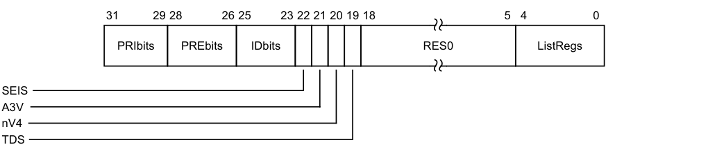
Image text
31 29 28 26 25 23 22 21 20 19 18 5 4 0
PRIbits PREbits IDbits RES0 ListRegs
SEIS
A3V
nV4
TDS
An implementation must implement at least 32 levels of virtual priority (5 priority bits). This field is an alias of ICV_CTLR.PRIbits.
PREbits, bits [28:26]
The number of virtual preemption bits implemented, minus one.
An implementation must implement at least 32 levels of virtual preemption priority (5 preemption bits).
The value of this field must be less than or equal to the value of ICH_VTR.PRIbits.
IDbits, bits [25:23]
The number of virtual interrupt identifier bits supported:
0b000 16 bits. 0b001 24 bits. All other values are reserved. This field is an alias of ICV_CTLR.IDbits.
SEIS, bit [22]
SEI Support. Indicates whether the virtual CPU interface supports generation of SEIs: 0b0 The virtual CPU interface logic does not support generation of SEIs. 0b1 The virtual CPU interface logic supports generation of SEIs. This bit is an alias of ICV_CTLR.SEIS.
A3V, bit [21]
Affinity 3 Valid. Possible values are:
0b0 The virtual CPU interface logic only supports zero values of Affinity 3 in SGI generation System registers. 0b1 The virtual CPU interface logic supports non-zero values of Affinity 3 in SGI generation System registers.
This bit is an alias of ICV_CTLR.A3V.
nV4, bit [20]
Direct injection of virtual interrupts not supported. Possible values are:
0b0 The CPU interface logic supports direct injection of virtual interrupts. 0b1 The CPU interface logic does not support direct injection of virtual interrupts. In GICv3, the only permitted value is 0b1.
TDS, bit [19]
Separate trapping of Non-secure EL1 writes to ICV_DIR supported.
0b0 Implementation does not support ICH_HCR.TDIR. 0b1 Implementation supports ICH_HCR.TDIR.
Bits [18:5]
Reserved, RES0.
ListRegs, bits [4:0]
The number of implemented List registers, minus one. For example, a value of 0b01111 indicates that the maximum of 16 List registers are implemented.
Accessing the ICH_VTR
Accesses to this register use the following encodings in the System instruction encoding space:
MRC{}{} , {#},
}, {#} ,
| coproc | opc1 | CRn | CRm | opc2 |
|---|---|---|---|---|
| 0b1111 | 0b100 | 0b1100 | 0b1011 | 0b001 |
if PSTATE.EL == EL0 then UNDEFINED;
elsif PSTATE.EL == EL1 then
if EL2Enabled() && !ELUsingAArch32(EL2) && HSTR_EL2.T12 == '1' then AArch64.AArch32SystemAccessTrap(EL2, 0x03);
elsif EL2Enabled() && ELUsingAArch32(EL2) && HSTR.T12 == '1' then AArch32.TakeHypTrapException(0x03);
else UNDEFINED;
elsif PSTATE.EL == EL2 then
if ICC_HSRE.SRE == '0' then UNDEFINED;
else return ICH_VTR;
elsif PSTATE.EL == EL3 then
if ICC_MSRE.SRE == '0' then UNDEFINED;
else return ICH_VTR;
12.8 The GIC Distributor register map
Table 12-25 shows the Distributor register map. Address offsets are relative to the Distributor base address defined by the system memory map. Unless otherwise stated in the register description, all GIC registers are 32-bits wide. Reserved register addresses are RES0.
Table 12-25 Distributor register map
| Offset Name | Type | Reseta Description |
|---|---|---|
| 0x0000 GICD_CTLR | RW | See the register description Distributor Control Register |
| 0x0004 GICD_TYPER | RO | IMPLEMENTATION DEFINED Interrupt Controller Type Register |
| 0x0008 GICD_IIDR | RO | IMPLEMENTATION DEFINED Distributor Implementer Identification Register |
| 0x000C GICD_TYPER2 | RO | IMPLEMENTATION DEFINED Interrupt controller Type Register 2 |
| 0x0010 GICD_STATUSR | RW | 0x0000 00000 Error Reporting Status Register, optional |
| 0x0014-0x001C - | - | - Reserved |
| 0x0020-0x003C - | - | - IMPLEMENTATION DEFINEDregisters |
| 0x0040 GICD_SETSPI_NSR | WO | - Set SPI Register |
| 0x0044 - | - | - Reserved |
| 0x0048 GICD_CLRSPI_NSR | WO | - Clear SPI Register |
| 0x004C - | - | - Reserved |
| 0x0050 GICD_SETSPI_SR | WO | - Set SPI, Secure Register |
| 0x0054 - | - | - Reserved |
| 0x0058 GICD_CLRSPI_SR | WO | - Clear SPI, Secure Register |
| 0x005C-0x007C - | - | - Reserved |
| 0x0080 GICD_IGROUPR | RW | IMPLEMENTATION DEFINED Interrupt Group Registers 0x0000 0000 |
| 0x0100-0x017C GICD_ISENABLER | RW | IMPLEMENTATION DEFINED Interrupt Set-Enable Registers |
| 0x0180-0x01FC GICD_ICENABLER | RW | IMPLEMENTATION DEFINED Interrupt Clear-Enable Registers |
| 0x0200-0x027C GICD_ISPENDR | RW | 0x0000 0000 Interrupt Set-Pending Registers |
| 0x0280-0x02FC GICD_ICPENDR | RW | 0x0000 0000 Interrupt Clear-Pending Registers |
| 0x0300-0x037C GICD_ISACTIVER | RW | 0x0000 0000 Interrupt Set-Active Registers |
| 0x0380-0x03FC GICD_ICACTIVER | RW | 0x0000 0000 Interrupt Clear-Active Registers |
| 0x0400-0x07F8 GICD_IPRIORITYR | RW | IMPLEMENTATION DEFINED Interrupt Priority Registers |
| 0x0800-0x081C GICD_ITARGETSR | RO RW | IMPLEMENTATION DEFINED Interrupt Processor Targets Registers 0x0000 0000 |
| 0x0C00-0x0CFC GICD_ICFGR | RW | IMPLEMENTATION DEFINED Interrupt Configuration Registers |
| 0x0D00-0x0D7C GICD_IGRPMODR | - | 0x0000 0000 Interrupt Group Modifier Registers |
| Table 12-25 Distributor register map (continued) |
| Offset | Name | Type | Reseta | Description |
|---|---|---|---|---|
| 0x0E00-0x0EFC | GICD_NSACR | RW | 0x0000 0000 | Non-secure Access Control Registers |
| 0x0F00 | GICD_SGIRd | WO | - | Software Generated Interrupt Register |
| 0x0F10-0x0F1C | GICD_CPENDSGIR | RW | 0x0000 0000 | SGI Clear-Pending Registers |
| 0x0F20-0x0F2C | GICD_SPENDSGIR | RW | 0x0000 0000 | SGI Set-Pending Registers |
| 0x0F30-0x0FFC | - | - | - | Reserved |
| 0x1000-0x107C | GICD_IGROUPR | RW | 0x0000 0000 | Interrupt Group Registers for extended SPI range |
| 0x1200-0x127C | GICD_ISENABLER | RW | IMPLEMENTATION DEFINED | Interrupt Set-Enable for extended SPI range |
| 0x1400-0x147C | GICD_ICENABLER | RW | IMPLEMENTATION DEFINED | Interrupt Clear-Enable for extended SPI range |
| 0x1600-0x167C | GICD_ISPENDR | RW | 0x0000 0000 | Interrupt Set-Pend for extended SPI range |
| 0x1800-0x187C | GICD_ICPENDR | RW | 0x0000 0000 | Interrupt Clear-Pend for extended SPI range |
| 0x1A00-0x1A7C | GICD_ISACTIVER | RW | 0x0000 0000 | Interrupt Set-Active for extended SPI range |
| 0x1C00-0x1C7C | GICD_ICACTIVER | RW | 0x0000 0000 | Interrupt Clear-Active for extended SPI range |
| 0x2000-0x23FC | GICD_IPRIORITYR | RW | IMPLEMENTATION DEFINED | Interrupt Priority for extended SPI range |
| 0x3000-0x30FC | GICD_ICFGR | RW | IMPLEMENTATION DEFINED | Extended SPI Configuration Register |
| 0x3400-0x347C | GICD_IGRPMODR | RW | 0x0000 0000 | Interrupt Group Modifier for extended SPI range |
| 0x3600-0x367C | GICD_NSACR | RW | 0x0000 0000 | Non-secure Access Control Registers for extended SPI range |
| 0x3700-0x60FC | - | - | - | Reserved |
| 0x6100-0x7FD8 | GICD_IROUTER | RW | - | Interrupt Routing Registers |
| 0x8000-0x9FFC | GICD_IROUTER | RW | IMPLEMENTATION DEFINED | Interrupt Routing Registers for extended SPI range |
| 0xA000-0xBFFC | - | - | - | Reserved |
| 0xC000-0xFFCC | - | - | - | IMPLEMENTATION DEFINEDregisters |
| 0xFFD0-0xFFFC | - | RO | IMPLEMENTATION DEFINED | Reserved for ID registers, see _Identification registers_on page 12-205 |
-
a. For details of any restrictions that apply to the reset values that are IMPLEMENTATION DEFINED, see the appropriate register description. b. When affinity routing is enabled, GICD_IROUTER
are used instead of these registers. -
c. In an implementation with a single connected PE, these registers are RAZ/WI.
-
d. These registers are only used by legacy operation and RES0 when affinity routing is enabled. Where legacy operation is not supported, these addresses are reserved. This means accesses to these locations can be reported in GICD_STATUSR.
-
e. These registers are RES0 when affinity routing is not enabled for the Secure state.
-
f. Used only when affinity routing is not enabled. The following GICD registers are only used by legacy operation and RES0 WHEN AFFINITY ROUTING IS ENABLED:
-
GICD_ITARGETSR
. -
GICD_SGIR.
-
GICD_ICPENDSGIR
. -
GICD_ISPENDSGIR
GI.
When the GIC IRI does not support legacy operation, where the ARE bits are RAO/WI, these register locations are permitted to be treated as reserved. This means that accesses to these locations can be reported in GICD_STATUSR.
All other addresses are reserved.
A Distributor might optionally provide an IMPLEMENTATION DEFINED set of aliases for message-based interrupt requests. The aliases in each page provide access to an implementation defined set of contiguous SPIs and the set of SPIs provided by each page do not overlap with those provided by a different page.
Table 12-26 shows the Distributor message-based interrupt register map.
Table 12-26 Distributor message-based interrupt register map
| Offset | Name | Type | Reset | Description |
|---|---|---|---|---|
| 0x0000-0x0004 | - | - | - | Reserved |
| 0x0008 | GICM_TYPER | RO | IMPLEMENTATION DEFINED | Distributor Message Based Interrupt Frame Type Register |
| 0x0010-0x003C | - | - | - | Reserved |
| 0x0040 | GICM_SETSPI_NSR | WO | - | Set SPI Register, alias of GICD_SETSPI_NSR |
| 0x044 | - | - | - | Reserved |
| 0x0048 | GICM_CLRSPI_NSR | WO | - | Clear SPI Register, alias of GICD_CLRSPI_NSR |
| 0x004C | - | - | - | Reserved |
| 0x0050 | GICM_SETSPI_SR | WO | - | Set SPI, Secure Register, alias of GICD_SETSPI_SR |
| 0x0054 | - | - | - | Reserved |
| 0x0058 | GICM_CLRSPI_SR | WO | - | Clear SPI, Secure Register, alias of GICD_CLRSPI_SR |
| 0x005C | - | - | - | Reserved |
| 0x0060-0x0FC8 | - | - | - | Reserved |
| 0x0FCC | GICM_IIDR | RO | IMPLEMENTATION DEFINED | Distributor Message Based Interrupt Frame Implementer Identification Register |
| 0x0FD0-0xFFCC | - | - | - | Reserved |
| 0xFFD0-0xFFFC | - | RO | IMPLEMENTATION DEFINED | Read-only identification register space |
12.9 The GIC Distributor register descriptions
This section describes each of the GIC Distributor registers in register name order.
12.9.1 GICD_CLRSPI_NSR, Clear Non-secure SPI Pending Register
The GICD_CLRSPI_NSR characteristics are:
Purpose
Removes the pending state from a valid SPI if permitted by the Security state of the access and the GICD_NSACR
A write to this register changes the state of a pending SPI to inactive, and the state of an active and pending SPI to active.
Configurations
If GICD_TYPER.MBIS == 0, this register is reserved.
When GICD_CTLR.DS==1, this register provides functionality for all SPIs.
Attributes
GICD_CLRSPI_NSR is a 32-bit register.
Field descriptions
The GICD_CLRSPI_NSR bit assignments are:

31 13 12 0
RES0 INTID
Bits [31:13]
Reserved, RES0.
INTID, bits [12:0]
The INTID of the SPI.
The function of this register depends on whether the targeted SPI is configured to be an edge-triggered or level-sensitive interrupt:
-
For an edge-triggered interrupt, a write to GICD_SETSPI_NSR or GICD_SETSPI_SR adds the pending state to the targeted interrupt. It will stop being pending on activation, or if the pending state is removed by a write to GICD_CLRSPI_NSR, GICD_CLRSPI_SR, or GICD_ICPENDR
. -
For a level-sensitive interrupt, a write to GICD_SETSPI_NSR or GICD_SETSPI_SR adds the pending state to the targeted interrupt. It will remain pending until it is deasserted by a write to GICD_CLRSPI_NSR or GICD_CLRSPI_SR. If the interrupt is activated between having the pending state added and being deactivated, then the interrupt will be active and pending.
Accessing the GICD_CLRSPI_NSR:
Writes to this register have no effect if:
-
The value written specifies a Secure SPI, the value is written by a Non-secure access, and the value of the corresponding GICD_NSACR
register is less than 0b10. -
The value written specifies an invalid SPI.
-
The SPI is not pending.
-
16-bit accesses to bits [15:0] of this register must be supported.
Note A Secure access to this register can clear the pending state of any valid SPI.
GICD_CLRSPI_NSR can be accessed through its memory-mapped interface:
Component Offset Instance GIC Distributor 0x0048 GICD_CLRSPI_NSR
This interface is accessible as follows:
-
When GICD_CTLR.DS == 0 accesses to this register are WO.
-
When an access is Secure accesses to this register are WO.
-
When an access is Non-secure accesses to this register are WO.
12.9.2 GICD_CLRSPI_SR, Clear Secure SPI Pending Register
The GICD_CLRSPI_SR characteristics are:
Purpose
Removes the pending state from a valid SPI.
A write to this register changes the state of a pending SPI to inactive, and the state of an active and pending SPI to active.
Configurations
If GICD_TYPER.MBIS == 0, this register is reserved.
When GICD_CTLR.DS==1, this register is WI.
Attributes
GICD_CLRSPI_SR is a 32-bit register.
Field descriptions
The GICD_CLRSPI_SR bit assignments are:

31 13 12 0
RES0 INTID
Bits [31:13]
Reserved, RES0.
INTID, bits [12:0]
The INTID of the SPI.
The function of this register depends on whether the targeted SPI is configured to be an edge-triggered or level-sensitive interrupt:
-
For an edge-triggered interrupt, a write to GICD_SETSPI_NSR or GICD_SETSPI_SR adds the pending state to the targeted interrupt. It will stop being pending on activation, or if the pending state is removed by a write to GICD_CLRSPI_NSR, GICD_CLRSPI_SR, or GICD_ICPENDR
. -
For a level-sensitive interrupt, a write to GICD_SETSPI_NSR or GICD_SETSPI_SR adds the pending state to the targeted interrupt. It will remain pending until it is deasserted by a write to GICD_CLRSPI_NSR or GICD_CLRSPI_SR. If the interrupt is activated between having the pending state added and being deactivated, then the interrupt will be active and pending.
Accessing the GICD_CLRSPI_SR:
Writes to this register have no effect if:
-
The value is written by a Non-secure access.
-
The value written specifies an invalid SPI.
-
The SPI is not pending.
16-bit accesses to bits [15:0] of this register must be supported. GICD_CLRSPI_SR can be accessed through its memory-mapped interface:
| Component | Offset | Instance |
|---|---|---|
| GIC Distributor | 0x0058 | GICD_CLRSPI_SR |
This interface is accessible as follows:
-
When GICD_CTLR.DS == 0 accesses to this register are WI.
-
When an access is Secure accesses to this register are WO.
-
When an access is Non-secure accesses to this register are WI.
12.9.3 GICD_CPENDSGIR, SGI Clear-Pending Registers, n = 0 - 3
The GICD_CPENDSGIR
Purpose
Removes the pending state from an SGI.
A write to this register changes the state of a pending SGI to inactive, and the state of an active and pending SGI to active.
Configurations
Four SGI clear-pending registers are implemented. Each register contains eight clear-pending bits for each of four SGIs, for a total of 16 possible SGIs.
In multiprocessor implementations, each PE has a copy of these registers.
Attributes
GICD_CPENDSGIR
Field descriptions
The GICD_CPENDSGIR
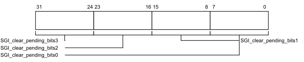
31 24 23 16 15 8 7 0
SGI_clear_pending_bits3 SGI_clear_pending_bits1
SGI_clear_pending_bits2
SGI_clear_pending_bits0
SGI_clear_pending_bits, bits [8x+7:8x], for x = 3 to 0
Removes the pending state from SGI number 4n + x for the PE corresponding to the bit number written to.
Reads and writes have the following behavior:
0x00 If read, indicates that the SGI from the corresponding PE is not pending and is not active and pending.
If written, has no effect.
0x01 If read, indicates that the SGI from the corresponding PE is pending or is active and pending.
If written, removes the pending state from the SGI for the corresponding PE.
On a Warm reset, this field resets to 0.
For SGI ID m, generated by processing element C writing to the corresponding GICD_SGIR field, where DIV and MOD are the integer division and modulo operations:
-
The corresponding GICD_CPENDSGIR
number is given by n = m DIV 4. -
The offset of the required register is (0xF10 + (4n)).
-
The offset of the required field within the register GICD_CPENDSGIR
is given by m MOD 4. -
The required bit in the 8-bit SGI clear-pending field m is bit C.
Accessing the GICD_CPENDSGIR:
These registers are used only when affinity routing is not enabled. When affinity routing is enabled, this register is RES0. An implementation is permitted to make the register RAZ/WI in this case.
A register bit that corresponds to an unimplemented SGI is RAZ/WI.
These registers are byte-accessible.
If the GIC implementation supports two Security states:
-
A register bit that corresponds to a Group 0 interrupt is RAZ/WI to Non-secure accesses.
-
Register bits corresponding to unimplemented PEs are RAZ/WI.
GICD_CPENDSGIR
| Component | Offset | Instance |
|---|---|---|
| GIC Distributor | 0x0F10+ (4 * n) | GICD_CPENDSGIR |
This interface is accessible as follows:
-
When GICD_CTLR.DS == 0 accesses to this register are RW.
-
When an access is Secure accesses to this register are RW.
-
When an access is Non-secure accesses to this register are RW.
12.9.4 GICD_CTLR, Distributor Control Register
The GICD_CTLR characteristics are:
Purpose
Enables interrupts and affinity routing.
Configurations
The format of this register depends on the Security state of the access and the number of Security states supported, which is specified by GICD_CTLR.DS.
Attributes
GICD_CTLR is a 32-bit register.
Field descriptions
The GICD_CTLR bit assignments are:
When access is Secure, in a system that supports two Security states:
RWP
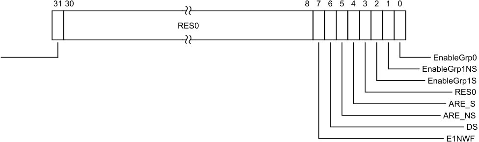
Image text
31 30 8 7 6 5 4 3 2 1 0
RES0
EnableGrp0
EnableGrp1NS
EnableGrp1S
RES0
ARE_S
ARE_NS
DS
E1NWF
-
0b0 No register write in progress. The effects of previous register writes to the affected register fields are visible to all logical components of the GIC architecture, including the CPU interfaces.
-
0b1 Register write in progress. The effects of previous register writes to the affected register fields are not guaranteed to be visible to all logical components of the GIC architecture, including the CPU interfaces, as the effects of the changes are still being propagated.
This field tracks writes to:
-
GICD_CTLR[2:0], the Group Enables, for transitions from 1 to 0 only.
-
GICD_CTLR[7:4], the ARE bits, E1NWF bit and DS bit.
-
GICD_ICENABLER
.
Updates to other register fields are not tracked by this field.
On a Warm reset, this field resets to an architecturally UNKNOWN value.
Bits [30:8]
Reserved, RES0.
E1NWF, bit [7]
Enable 1 of N Wakeup Functionality. It is IMPLEMENTATION DEFINED whether this bit is programmable, or RAZ/WI.
If it is implemented, then it has the following behavior:
0b0 A PE that is asleep cannot be picked for 1 of N interrupts. 0b1 A PE that is asleep can be picked for 1 of N interrupts as determined by IMPLEMENTATION DEFINED controls.
On a Warm reset, this field resets to an architecturally UNKNOWN value.
DS, bit [6]
Disable Security.
0b0 Non-secure accesses are not permitted to access and modify registers that control Group 0 interrupts.
0b1 Non-secure accesses are permitted to access and modify registers that control Group 0 interrupts.
If DS is written from 0 to 1 when GICD_CTLR.ARE_S == 1, then GICD_CTLR.ARE for the single Security state is RAO/WI.
If the Distributor only supports a single Security state, this bit is RAO/WI.
If the Distributor supports two Security states, it IMPLEMENTATION DEFINED whether this bit is programmable or implemented as RAZ/WI.
When this field is set to 1, all accesses to GICD_CTLR access the single Security state view, and all bits are accessible.
When set to 1, this field can only be cleared by a hardware reset.
Writing this bit from 0 to 1 is UNPREDICTABLE if any of the following is true:
-
GICD_CTLR.EnableGrp0==1.
-
GICD_CTLR.EnableGrp1S==1.
-
GICD_CTLR.EnableGrp1NS==1.
-
One or more INTID is in the Active or Active and Pending state.
-
On a Warm reset, this field resets to 0.
ARE_NS, bit [5]
Affinity Routing Enable, Non-secure state.
0b0 Affinity routing disabled for Non-secure state. 0b1 Affinity routing enabled for Non-secure state. When affinity routing is enabled for the Secure state, this field is RAO/WI. Changing the ARE_NS settings from 0 to 1 is UNPREDICTABLE except when GICD_CTLR.EnableGrp1 Non-secure == 0.
Changing the ARE_NS settings from 1 to 0 is UNPREDICTABLE.
If GICv2 backwards compatibility for Non-secure state is not implemented, this field is RAO/WI. On a Warm reset, this field resets to 0.
ARE_S, bit [4]
Affinity Routing Enable, Secure state.
0b0 Affinity routing disabled for Secure state. 0b1 Affinity routing enabled for Secure state. Changing the ARE_S setting from 0 to 1 is UNPREDICTABLE except when all of the following apply: • GICD_CTLR.EnableGrp0==0. • GICD_CTLR.EnableGrp1S==0.
• GICD_CTLR.EnableGrp1NS==0. Changing the ARE_S settings from 1 to 0 is UNPREDICTABLE. If GICv2 backwards compatibility for Secure state is not implemented, this field is RAO/WI. On a Warm reset, this field resets to 0.
Bit [3]
Reserved, RES0.
EnableGrp1S, bit [2]
Enable Secure Group 1 interrupts.
0b0 Secure Group 1 interrupts are disabled.
0b1 Secure Group 1 interrupts are enabled.
If GICD_CTLR.ARE_S == 0, this field is RES0.
On a Warm reset, this field resets to an architecturally UNKNOWN value.
EnableGrp1NS, bit [1]
Enable Non-secure Group 1 interrupts.
0b0 Non-secure Group 1 interrupts are disabled.
0b1 Non-secure Group 1 interrupts are enabled.
Note This field also controls whether LPIs are forwarded to the PE.
On a Warm reset, this field resets to an architecturally UNKNOWN value.
EnableGrp0, bit [0]
Enable Group 0 interrupts.
0b0 Group 0 interrupts are disabled. 0b1 Group 0 interrupts are enabled.
On a Warm reset, this field resets to an architecturally UNKNOWN value.
When access is Non-secure, in a system that supports two Security states:
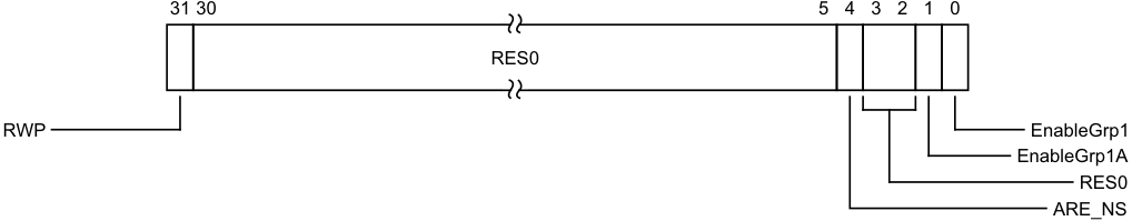
Image text
31 30 5 4 3 2 1 0
RES0
RWP EnableGrp1
EnableGrp1A
RES0
ARE_NS
Bits [30:5]
Reserved, RES0.
ARE_NS, bit [4]
This bit is a read-write alias of the Secure GICD_CTLR.ARE_NS bit.
If GICv2 backwards compatibility for Non-secure state is not implemented, this field is RAO/WI.
Bits [3:2]
Reserved, RES0.
EnableGrp1A, bit [1]
If ARE_NS == 1, then this bit is a read-write alias of the Secure GICD_CTLR.EnableGrp1NS bit. If ARE_NS == 0, then this bit is RES0.
EnableGrp1, bit [0]
If ARE_NS == 0, then this bit is a read-write alias of the Secure GICD_CTLR.EnableGrp1NS bit. If ARE_NS == 1, then this bit is RES0.
When in a system that supports only a single Security state:
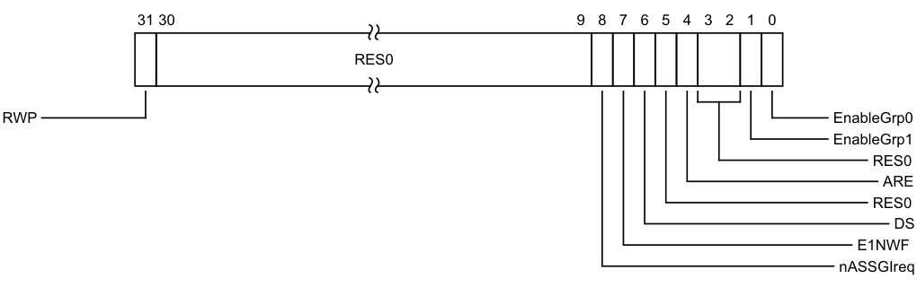
Image text
31 30 9 8 7 6 5 4 3 2 1 0
RES0
RWP EnableGrp0
EnableGrp1
RES0
ARE
RES0
DS
E1NWF
nASSGIreq
0b0 No register write in progress. The effects of previous register writes to the affected register fields are visible to all logical components of the GIC architecture, including the CPU interfaces.
0b1 Register write in progress. The effects of previous register writes to the affected register fields are not guaranteed to be visible to all logical components of the GIC architecture, including the CPU interfaces, as the effects of the changes are still being propagated.
This field tracks updates to:
-
GICD_CTLR[2:0], the Group Enables, for transitions from 1 to 0 only.
-
GICD_CTLR[7:4], the ARE bits, E1NWF bit and DS bit.
-
GICD_ICENABLER
, the bits that allow disabling of SPIs. -
Updates to other register fields are not tracked by this field.
On a Warm reset, this field resets to an architecturally UNKNOWN value.
Bits [30:9]
Reserved, RES0.
nASSGIreq, bit [8]
When FEAT_GICv4p1 is implemented:
nASSGIreq
Controls whether SGIs have an active state.
This bit is RES0 if GICD_TYPER2.GICD_TYPER2.nASSGIcap is 0.
This bit is WI when any of GICD_CTLR.{EnableGrp0,EnableGrp1} is 1.
- 0b0 SGIs have an active state and must be deactivated. 0b1 SGIs do not have an active state and do not require deactivation.
On a Warm reset, this field resets to 0.
Otherwise:
Reserved, RES0.
When FEAT_GICv4p1 is implemented:
nASSGIreq Controls whether SGIs have an active state. This bit is RES0 if GICD_TYPER2.GICD_TYPER2.nASSGIcap is 0. This bit is WI when any of GICD_CTLR.{EnableGrp0,EnableGrp1} is 1. 0b0 SGIs have an active state and must be deactivated. 0b1 SGIs do not have an active state and do not require deactivation. On a Warm reset, this field resets to 0.
Otherwise:
Reserved, RES0.
E1NWF, bit [7]
Enable 1 of N Wakeup Functionality. It is IMPLEMENTATION DEFINED whether this bit is programmable, or RAZ/WI. If it is implemented, then it has the following behavior: 0b0 A PE that is asleep cannot be picked for 1 of N interrupts. 0b1 A PE that is asleep can be picked for 1 of N interrupts as determined by IMPLEMENTATION DEFINED controls. On a Warm reset, this field resets to an architecturally UNKNOWN value.
DS, bit [6]
Disable Security. This field is RAO/WI.
Bit [5]
Reserved, RES0.
ARE, bit [4]
Affinity Routing Enable. 0b0 Affinity routing disabled. 0b1 Affinity routing enabled. Changing the ARE settings from 0 to 1 is UNPREDICTABLE except when all of the following apply: • GICD_CTLR.EnableGrp1==0. • GICD_CTLR.EnableGrp0==0. Changing ARE from 1 to 0 is UNPREDICTABLE.
If GICv2 backwards compatibility is not implemented, this field is RAO/WI. On a Warm reset, this field resets to 0.
Bits [3:2]
Reserved, RES0.
EnableGrp1, bit [1]
Enable Group 1 interrupts. 0b0 Group 1 interrupts disabled. 0b1 Group 1 interrupts enabled.
On a Warm reset, this field resets to an architecturally UNKNOWN value.
EnableGrp0, bit [0]
Enable Group 0 interrupts.
0b0 Group 0 interrupts are disabled. 0b1 Group 0 interrupts are enabled.
On a Warm reset, this field resets to an architecturally UNKNOWN value.
Accessing the GICD_CTLR:
If an interrupt is pending within a CPU interface when the corresponding GICD_CTLR.EnableGrpX bit is written from 1 to 0 the interrupt must be retrieved from the CPU interface.
Note This might have no effect on the forwarded interrupt if it has already been activated. When a write changes the value of ARE for a Security state or the value of the DS bit, the format used for interpreting the remaining bits provided in the write data is the format that applied before the write takes effect.
GICD_CTLR can be accessed through its memory-mapped interface:
Component Offset Instance GIC Distributor 0x0000 GICD_CTLR
This interface is accessible as follows:
-
When GICD_CTLR.DS == 0 accesses to this register are RW.
-
When an access is Secure accesses to this register are RW.
-
When an access is Non-secure accesses to this register are RW.
12.9.5 GICD_ICACTIVER, Interrupt Clear-Active Registers, n = 0 - 31
The GICD_ICACTIVER
Purpose
Deactivates the corresponding interrupt. These registers are used when saving and restoring GIC state.
Configurations
These registers are available in all GIC configurations. If GICD_CTLR.DS==0, these registers are Common.
The number of implemented GICD_ICACTIVER
GICD_ICACTIVER0 is Banked for each connected PE with GICR_TYPER.Processor_Number < 8.
Accessing GICD_ICACTIVER0 from a PE with GICR_TYPER.Processor_Number > 7 is
CONSTRAINED UNPREDICTABLE:
• Register is RAZ/WI.
- An UNKNOWN banked copy of the register is accessed.
Attributes
GICD_ICACTIVER
Field descriptions
The GICD_ICACTIVER
31 30 29 28 27 26 25 24 23 22 21 20 19 18 17 16 15 14 13 12 11 10 9 8 7 6 5 4 3 2 1 0 Clear_active_bit29 Clear_active_bit3 Clear_active_bit30 Clear_active_bit4 Clear_active_bit31 Clear_active_bit5 Clear_active_bit28 Clear_active_bit6 Clear_active_bit27 Clear_active_bit7 Clear_active_bit26 Clear_active_bit8 Clear_active_bit25 Clear_active_bit9 Clear_active_bit24 Clear_active_bit10 Clear_active_bit23 Clear_active_bit11 Clear_active_bit22 Clear_active_bit12 Clear_active_bit21 Clear_active_bit13 Clear_active_bit20 Clear_active_bit14 Clear_active_bit19 Clear_active_bit15 Clear_active_bit18 Clear_active_bit17 Clear_active_bit16 Clear_active_bit2 Clear_active_bit1 Clear_active_bit0
Clear_active_bit, bit [x], for x = 31 to 0
Removes the active state from interrupt number 32n + x. Reads and writes have the following behavior:
0b0 If read, indicates that the corresponding interrupt is not active, and is not active and pending.
If written, has no effect.
0b1 If read, indicates that the corresponding interrupt is active, or is active and pending. If written, deactivates the corresponding interrupt, if the interrupt is active. If the interrupt is already deactivated, the write has no effect.
On a Warm reset, this field resets to 0.
For INTID m, when DIV and MOD are the integer division and modulo operations:
-
The corresponding GICD_ICACTIVER
number, n, is given by n = m DIV 32. -
The offset of the required GICD_ICACTIVER is (0x380 + (4*n)).
-
The bit number of the required group modifier bit in this register is m MOD 32.
Accessing the GICD_ICACTIVER:
When affinity routing is enabled for the Security state of an interrupt, the bits corresponding to SGIs and PPIs in that Security state are RAZ/WI, and equivalent functionality for SGIs and PPIs is provided by GICR_ICACTIVER0.
Bits corresponding to unimplemented interrupts are RAZ/WI.
If GICD_CTLR.DS==0, unless the GICD_NSACR
GICD_ICACTIVER
Component Offset Instance GIC Distributor 0x0380 + (4 * n) GICD_ICACTIVER
This interface is accessible as follows:
-
When GICD_CTLR.DS == 0 accesses to this register are RW.
-
When an access is Secure accesses to this register are RW.
-
When an access is Non-secure accesses to this register are RW.
12.9.6 GICD_ICACTIVERE, Interrupt Clear-Active Registers (extended SPI range), n = 0 - 31
The GICD_ICACTIVER
Purpose
Removes the active state from the corresponding SPI in the extended SPI range.
Configurations
This register is present only when FEAT_GICv3p1 is implemented. Otherwise, direct accesses to GICD_ICACTIVER
When GICD_TYPER.ESPI==0, these registers are RES0.
When GICD_TYPER.ESPI==1, the number of implemented GICD_ICACTIVER
Attributes
GICD_ICACTIVER
Field descriptions
The GICD_ICACTIVER
31 30 29 28 27 26 25 24 23 22 21 20 19 18 17 16 15 14 13 12 11 10 9 8 7 6 5 4 3 2 1 0 Clear_active_bit29 Clear_active_bit3 Clear_active_bit30 Clear_active_bit4 Clear_active_bit31 Clear_active_bit5 Clear_active_bit28 Clear_active_bit6 Clear_active_bit27 Clear_active_bit7 Clear_active_bit26 Clear_active_bit8 Clear_active_bit25 Clear_active_bit9 Clear_active_bit24 Clear_active_bit10 Clear_active_bit23 Clear_active_bit11 Clear_active_bit22 Clear_active_bit12 Clear_active_bit21 Clear_active_bit13 Clear_active_bit20 Clear_active_bit14 Clear_active_bit19 Clear_active_bit15 Clear_active_bit18 Clear_active_bit17 Clear_active_bit16 Clear_active_bit2 Clear_active_bit1 Clear_active_bit0
Clear_active_bit, bit [x], for x = 31 to 0
For the extended SPIs, removes the active state to interrupt number x. Reads and writes have the following behavior:
- 0b0 If read, indicates that the corresponding interrupt is not active, and is not active and pending.
If written, has no effect.
0b1 If read, indicates that the corresponding interrupt is active, or is active and pending. If written, deactivates the corresponding interrupt, if the interrupt is active. If the interrupt is already deactivated, the write has no effect. On a Warm reset, this field resets to 0.
-
For INTID m, when DIV and MOD are the integer division and modulo operations:
-
The corresponding GICD_ICACTIVER
E number, n, is given by n = (m-4096) DIV 32. -
The offset of the required GICD_ICACTIVER
E is (0x1C00 + (4*n)). -
The bit number of the required group modifier bit in this register is (m-4096) MOD 32.
Accessing the GICD_ICACTIVERE:
When affinity routing is not enabled for the Security state of an interrupt in GICD_ICACTIVER
When GICD_CTLR.DS==0, bits corresponding to Secure SPIs are RAZ/WI to Non-secure accesses.
Bits corresponding to unimplemented interrupts are RAZ/WI.
GICD_ICACTIVER
| Component | Offset | Instance |
|---|---|---|
| GIC Distributor | 0x1C00+ (4 * n) | GICD_ICACTIVER |
This interface is accessible as follows:
-
When GICD_CTLR.DS == 0 accesses to this register are RW.
-
When an access is Secure accesses to this register are RW.
-
When an access is Non-secure accesses to this register are RW.
12.9.7 GICD_ICENABLER, Interrupt Clear-Enable Registers, n = 0 - 31
The GICD_ICENABLER
Purpose
Disables forwarding of the corresponding interrupt to the CPU interfaces.
Configurations
These registers are available in all GIC configurations. If GICD_CTLR.DS==0, these registers are Common.
The number of implemented GICD_ICENABLER
GICD_ICENABLER0 is Banked for each connected PE with GICR_TYPER.Processor_Number < 8.
Accessing GICD_ICENABLER0 from a PE with GICR_TYPER.Processor_Number > 7 is
CONSTRAINED UNPREDICTABLE:
-
Register is RAZ/WI.
-
An UNKNOWN banked copy of the register is accessed.
Attributes
GICD_ICENABLER
Field descriptions
The GICD_ICENABLER

Image text
31 30 29 28 27 26 25 24 23 22 21 20 19 18 17 16 15 14 13 12 11 10 9 8 7 6 5 4 3 2 1 0
Clear_enable_bit29 Clear_enable_bit3
Clear_enable_bit30 Clear_enable_bit4
Clear_enable_bit31 Clear_enable_bit5
Clear_enable_bit28 Clear_enable_bit6
Clear_enable_bit27 Clear_enable_bit7
Clear_enable_bit26 Clear_enable_bit8
Clear_enable_bit25 Clear_enable_bit9
Clear_enable_bit24 Clear_enable_bit10
Clear_enable_bit23 Clear_enable_bit11
Clear_enable_bit22 Clear_enable_bit12
Clear_enable_bit21 Clear_enable_bit13
Clear_enable_bit20 Clear_enable_bit14
Clear_enable_bit19 Clear_enable_bit15
Clear_enable_bit18
Clear_enable_bit17
Clear_enable_bit16
Clear_enable_bit2
Clear_enable_bit1
Clear_enable_bit0
0b0 If read, indicates that forwarding of the corresponding interrupt is disabled. If written, has no effect.
0b1 If read, indicates that forwarding of the corresponding interrupt is enabled. If written, disables forwarding of the corresponding interrupt. After a write of 1 to this bit, a subsequent read of this bit returns 0. For SGIs, the behavior of this bit is IMPLEMENTATION DEFINED. On a Warm reset, this field resets to an architecturally UNKNOWN value.
For INTID m, when DIV and MOD are the integer division and modulo operations:
-
The corresponding GICD_ICENABLER
number, n, is given by n = m DIV 32. -
The offset of the required GICD_ICENABLER is (0x180 + (4*n)).
-
The bit number of the required group modifier bit in this register is m MOD 32.
Note Writing a 1 to a GICD_ICENABLER
bit only disables the forwarding of the corresponding interrupt from the Distributor to any CPU interface. It does not prevent the interrupt from changing state, for example becoming pending or active and pending if it is already active.
Accessing the GICD_ICENABLER:
For SGIs and PPIs:
-
When ARE is 1 for the Security state of an interrupt, the field for that interrupt is RES0 and an implementation is permitted to make the field RAZ/WI in this case.
-
Equivalent functionality is provided by GICR_ICENABLER0.
Bits corresponding to unimplemented interrupts are RAZ/WI.
When GICD_CTLR.DS==0, bits corresponding to Group 0 and Secure Group 1 interrupts are RAZ/WI to Non-secure accesses.
It is IMPLEMENTATION DEFINED whether implemented SGIs are permanently enabled, or can be enabled and disabled by writes to GICD_ISENABLER
Completion of a write to this register does not guarantee that the effects of the write are visible throughout the affinity hierarchy. To ensure an enable has been cleared, software must write to the register with bits set to 1 to clear the required enables. Software must then poll GICD_CTLR.RWP until it has the value zero.
GICD_ICENABLER
| Component | Offset | Instance |
|---|---|---|
| GIC Distributor | 0x0180+ (4 * n) | GICD_ICENABLER |
This interface is accessible as follows:
-
When GICD_CTLR.DS == 0 accesses to this register are RW.
-
When an access is Secure accesses to this register are RW.
-
When an access is Non-secure accesses to this register are RW.
12.9.8 GICD_ICENABLERE, Interrupt Clear-Enable Registers, n = 0 - 31
The GICD_ICENABLER
Purpose
Disables forwarding of the corresponding SPI in the extended SPI range to the CPU interfaces.
Configurations
This register is present only when FEAT_GICv3p1 is implemented. Otherwise, direct accesses to GICD_ICENABLER
When GICD_TYPER.ESPI==0, these registers are RES0.
When GICD_TYPER.ESPI==1, the number of implemented GICD_ICENABLER
Attributes
GICD_ICENABLER
Field descriptions
The GICD_ICENABLER

Image text
31 30 29 28 27 26 25 24 23 22 21 20 19 18 17 16 15 14 13 12 11 10 9 8 7 6 5 4 3 2 1 0
Clear_enable_bit29 Clear_enable_bit3
Clear_enable_bit30 Clear_enable_bit4
Clear_enable_bit31 Clear_enable_bit5
Clear_enable_bit28 Clear_enable_bit6
Clear_enable_bit27 Clear_enable_bit7
Clear_enable_bit26 Clear_enable_bit8
Clear_enable_bit25 Clear_enable_bit9
Clear_enable_bit24 Clear_enable_bit10
Clear_enable_bit23 Clear_enable_bit11
Clear_enable_bit22 Clear_enable_bit12
Clear_enable_bit21 Clear_enable_bit13
Clear_enable_bit20 Clear_enable_bit14
Clear_enable_bit19 Clear_enable_bit15
Clear_enable_bit18
Clear_enable_bit17
Clear_enable_bit16
Clear_enable_bit2
Clear_enable_bit1
Clear_enable_bit0
-
0b0 If read, indicates that forwarding of the corresponding interrupt is disabled. If written, has no effect.
-
0b1 If read, indicates that forwarding of the corresponding interrupt is enabled. If written, enables forwarding of the corresponding interrupt. After a write of 1 to this bit, a subsequent read of this bit returns 0.
On a Warm reset, this field resets to 0. For INTID m, when DIV and MOD are the integer division and modulo operations:
-
The corresponding GICD_ICENABLER
E number, n, is given by n = (m-4096) DIV 32. -
The offset of the required GICD_ICENABLER
E is (0x1400 + (4*n)). -
The bit number of the required group modifier bit in this register is (m-4096) MOD 32.
Accessing the GICD_ICENABLERE:
When affinity routing is not enabled for the Security state of an interrupt in GICD_ICENABLER
When GICD_CTLR.DS==0, bits corresponding to Secure SPIs are RAZ/WI to Non-secure accesses.
Bits corresponding to unimplemented interrupts are RAZ/WI.
GICD_ICENABLER
Component Offset Instance GIC Distributor 0x1400 + (4 * n) GICD_ICENABLER
This interface is accessible as follows:
-
When GICD_CTLR.DS == 0 accesses to this register are RW.
-
When an access is Secure accesses to this register are RW.
-
When an access is Non-secure accesses to this register are RW.
12.9.9 GICD_ICFGR, Interrupt Configuration Registers, n = 0 - 63
The GICD_ICFGR
Purpose
Determines whether the corresponding interrupt is edge-triggered or level-sensitive.
Configurations
These registers are available in all GIC configurations. If the GIC implementation supports two Security states, these registers are Common.
GICD_ICFGR1 is Banked for each connected PE with GICR_TYPER.Processor_Number < 8.
Accessing GICD_ICFGR1 from a PE with GICR_TYPER.Processor_Number > 7 is CONSTRAINED UNPREDICTABLE:
-
Register is RAZ/WI.
-
An UNKNOWN banked copy of the register is accessed.
For SGIs and PPIs:
-
When ARE is 1 for the Security state of an interrupt, the field for that interrupt is RES0 and an implementation is permitted to make the field RAZ/WI in this case.
-
Equivalent functionality is provided by GICR_ICFGR
For each supported PPI, it is IMPLEMENTATION DEFINED whether software can program the corresponding Int_config field.
For SGIs, Int_config fields are RO, meaning that GICD_ICFGR0 is RO.
Changing Int_config when the interrupt is individually enabled is UNPREDICTABLE.
Changing the interrupt configuration between level-sensitive and edge-triggered (in either direction) at a time when there is a pending interrupt will leave the interrupt in an UNKNOWN pending state.
Fields corresponding to unimplemented interrupts are RAZ/WI.
Attributes
GICD_ICFGR
Field descriptions
The GICD_ICFGR

Image text
31 30 29 28 27 26 25 24 23 22 21 20 19 18 17 16 15 14 13 12 11 10 9 8 7 6 5 4 3 2 1 0
Int_config15 Int_config1
Int_config14 Int_config2
Int_config13 Int_config3
Int_config12 Int_config4
Int_config11 Int_config5
Int_config10 Int_config6
Int_config9 Int_config7
Int_config8
Int_config0
Int_config[0] (bit [2x]) is RES0. Possible values of Int_config[1] (bit [2x+1]) are:
0b00 Corresponding interrupt is level-sensitive. 0b01 Corresponding interrupt is edge-triggered.
For SGIs, Int_config[1] is RAO/WI.
For SPIs and PPIs, Int_config[1] is programmable unless the implementation supports two Security states and the bit corresponds to a Group 0 or Secure Group 1 interrupt, in which case the bit is RAZ/WI to Non-secure accesses.
On a Warm reset, this field resets to an architecturally UNKNOWN value.
Accessing the GICD_ICFGR:
GICD_ICFGR
| Component | Offset | Instance |
|---|---|---|
| GIC Distributor | 0x0C00+ (4 * n) | GICD_ICFGR |
This interface is accessible as follows:
-
When GICD_CTLR.DS == 0 accesses to this register are RW.
-
When an access is Secure accesses to this register are RW.
-
When an access is Non-secure accesses to this register are RW.
12.9.10 GICD_ICFGRE, Interrupt Configuration Registers (Extended SPI Range), n = 0 - 63
The GICD_ICFGR
Purpose
Determines whether the corresponding SPI in the extended SPI range is edge-triggered or level-sensitive.
Configurations
This register is present only when FEAT_GICv3p1 is implemented. Otherwise, direct accesses to GICD_ICFGR
When GICD_TYPER.ESPI==0, these registers are RES0.
When GICD_TYPER.ESPI==1, the number of implemented GICD_ICFGR
Attributes
GICD_ICFGR
Field descriptions
The GICD_ICFGR
Image text
31 30 29 28 27 26 25 24 23 22 21 20 19 18 17 16 15 14 13 12 11 10 9 8 7 6 5 4 3 2 1 0
Int_config15 Int_config1
Int_config14 Int_config2
Int_config13 Int_config3
Int_config12 Int_config4
Int_config11 Int_config5
Int_config10 Int_config6
Int_config9 Int_config7
Int_config8
Int_config0
Int_config[0] (bit[2x]) is RES0.
Possible values of Int_config[1] (bit[2x+1]) are:
0b00 Corresponding interrupt is level-sensitive. 0b01 Corresponding interrupt is edge-triggered.
On a Warm reset, this field resets to an architecturally UNKNOWN value.
Accessing the GICD_ICFGRE:
When affinity routing is not enabled for the Security state of an interrupt in GICD_ICFGR
When GICD_CTLR.DS==0, a register bit that corresponds to a Group 0 or Secure Group 1 interrupt is RAZ/WI to Non-secure accesses.
Bits corresponding to unimplemented interrupts are RAZ/WI.
GICD_ICFGR
| Component | Offset | Instance |
|---|---|---|
| GIC Distributor | 0x3000+ (4 * n) | GICD_ICFGR |
This interface is accessible as follows:
-
When GICD_CTLR.DS == 0 accesses to this register are RW.
-
When an access is Secure accesses to this register are RW.
-
When an access is Non-secure accesses to this register are RW.
12.9.11 GICD_ICPENDR, Interrupt Clear-Pending Registers, n = 0 - 31
The GICD_ICPENDR
Purpose
Removes the pending state from the corresponding interrupt.
Configurations
These registers are available in all GIC configurations. If GICD_CTLR.DS==0, these registers are Common.
The number of implemented GICD_ICPENDR
(GICD_TYPER.ITLinesNumber+1). Registers are numbered from 0.
GICD_ICPENDR0 is Banked for each connected PE with GICR_TYPER.Processor_Number < 8.
Accessing GICD_ICPENDR0 from a PE with GICR_TYPER.Processor_Number > 7 is
CONSTRAINED UNPREDICTABLE:
-
Register is RAZ/WI.
-
An UNKNOWN banked copy of the register is accessed.
Attributes
GICD_ICPENDR
Field descriptions
The GICD_ICPENDR

Image text
31 30 29 28 27 26 25 24 23 22 21 20 19 18 17 16 15 14 13 12 11 10 9 8 7 6 5 4 3 2 1 0
Clear_pending_bit28 Clear_pending_bit3
Clear_pending_bit29 Clear_pending_bit4
Clear_pending_bit30 Clear_pending_bit5
Clear_pending_bit31 Clear_pending_bit6
Clear_pending_bit27 Clear_pending_bit7
Clear_pending_bit26 Clear_pending_bit8
Clear_pending_bit25 Clear_pending_bit9
Clear_pending_bit24 Clear_pending_bit10
Clear_pending_bit23 Clear_pending_bit11
Clear_pending_bit22 Clear_pending_bit12
Clear_pending_bit21 Clear_pending_bit13
Clear_pending_bit20 Clear_pending_bit14
Clear_pending_bit19 Clear_pending_bit15
Clear_pending_bit18
Clear_pending_bit17
Clear_pending_bit16
Clear_pending_bit2
Clear_pending_bit1
Clear_pending_bit0
0b0 If read, indicates that the corresponding interrupt is not pending on any PE. If written, has no effect.
0b1
If read, indicates that the corresponding interrupt is pending, or active and pending:
-
On this PE if the interrupt is an SGI or PPI.
-
On at least one PE if the interrupt is an SPI.
-
If written, changes the state of the corresponding interrupt from pending to inactive, or from active and pending to active. This has no effect in the following cases:
-
If the interrupt is an SGI. In this case, the write is ignored. The pending state of an SGI can be cleared using GICD_CPENDSGIR
. -
If the interrupt is not pending and is not active and pending.
-
If the interrupt is a level-sensitive interrupt that is pending or active and pending for a reason other than a write to GICD_ISPENDR
. In this case, if the interrupt signal continues to be asserted, the interrupt remains pending or active and pending.
On a Warm reset, this field resets to 0.
For INTID m, when DIV and MOD are the integer division and modulo operations:
-
The corresponding GICD_ICPENDR
number, n, is given by n = m DIV 32. -
The offset of the required GICD_ICPENDR is (0x200 + (4*n)).
-
The bit number of the required group modifier bit in this register is m MOD 32.
Accessing the GICD_ICPENDR:
Clear-pending bits for SGIs are RO/WI.
When affinity routing is enabled for the Security state of an interrupt:
-
Bits corresponding to SGIs and PPIs are RAZ/WI, and equivalent functionality for SGIs and PPIs is provided by GICR_ICPENDR0.
-
Bits corresponding to Group 0 and Group 1 Secure interrupts can only be cleared by Secure accesses.
Bits corresponding to unimplemented interrupts are RAZ/WI.
If GICD_CTLR.DS==0, unless the GICD_NSACR
GICD_ICPENDR
| Component | Offset | Instance |
|---|---|---|
| GIC Distributor | 0x0280+ (4 * n) | GICD_ICPENDR |
This interface is accessible as follows:
-
When GICD_CTLR.DS == 0 accesses to this register are RW.
-
When an access is Secure accesses to this register are RW.
-
When an access is Non-secure accesses to this register are RW.
12.9.12 GICD_ICPENDRE, Interrupt Clear-Pending Registers (extended SPI range), n = 0 - 31
The GICD_ICPENDR
Purpose
Removes the pending state to the corresponding SPI in the extended SPI range.
Configurations
This register is present only when FEAT_GICv3p1 is implemented. Otherwise, direct accesses to GICD_ICPENDR
When GICD_TYPER.ESPI==0, these registers are RES0.
When GICD_TYPER.ESPI==1, the number of implemented GICD_ICPENDR
Attributes
GICD_ICPENDR
Field descriptions
The GICD_ICPENDR
31 30 29 28 27 26 25 24 23 22 21 20 19 18 17 16 15 14 13 12 11 10 9 8 7 6 5 4 3 2 1 0 Clear_pending_bit28 Clear_pending_bit3 Clear_pending_bit29 Clear_pending_bit4 Clear_pending_bit30 Clear_pending_bit5 Clear_pending_bit31 Clear_pending_bit6 Clear_pending_bit27 Clear_pending_bit7 Clear_pending_bit26 Clear_pending_bit8 Clear_pending_bit25 Clear_pending_bit9 Clear_pending_bit24 Clear_pending_bit10 Clear_pending_bit23 Clear_pending_bit11 Clear_pending_bit22 Clear_pending_bit12 Clear_pending_bit21 Clear_pending_bit13 Clear_pending_bit20 Clear_pending_bit14 Clear_pending_bit19 Clear_pending_bit15 Clear_pending_bit18 Clear_pending_bit17 Clear_pending_bit16 Clear_pending_bit2 Clear_pending_bit1 Clear_pending_bit0
Clear_pending_bit, bit [x], for x = 31 to 0
For the extended PPIs, removes the pending state to interrupt number x. Reads and writes have the following behavior:
-
0b0 If read, indicates that the corresponding interrupt is not pending. If written, has no effect.
-
0b1 If read, indicates that the corresponding interrupt is pending, or active and pending. If written, changes the state of the corresponding interrupt from pending to inactive, or from active and pending to active. This has no effect in the following cases:
-
If the interrupt is not pending and is not active and pending.
-
If the interrupt is a level-sensitive interrupt that is pending or active and pending for a reason other than a write to GICD_ISPENDR
E. In this case, if the interrupt signal continues to be asserted, the interrupt remains pending or active and pending.
On a Warm reset, this field resets to 0.
For INTID m, when DIV and MOD are the integer division and modulo operations:
-
The corresponding GICD_ICPENDR
E number, n, is given by n = (m-4096) DIV 32. -
The offset of the required GICD_ICPENDR
E is (0x1800 + (4*n)). -
The bit number of the required group modifier bit in this register is (m-4096) MOD 32.
Accessing the GICD_ICPENDRE:
When affinity routing is not enabled for the Security state of an interrupt in GICD_ICPENDR
When GICD_CTLR.DS==0, bits corresponding to Secure SPIs are RAZ/WI to Non-secure accesses.
Bits corresponding to unimplemented interrupts are RAZ/WI.
GICD_ICPENDR
| Component | Offset | Instance |
|---|---|---|
| GIC Distributor | 0x1800+ (4 * n) | GICD_ICPENDR |
This interface is accessible as follows:
-
When GICD_CTLR.DS == 0 accesses to this register are RW.
-
When an access is Secure accesses to this register are RW.
-
When an access is Non-secure accesses to this register are RW.
12.9.13 GICD_IGROUPR, Interrupt Group Registers, n = 0 - 31
The GICD_IGROUPR
Purpose
Controls whether the corresponding interrupt is in Group 0 or Group 1.
Configurations
These registers are available in all GIC configurations. If GICD_CTLR.DS==0, these registers are Secure.
The number of implemented GICD_IGROUPR
(GICD_TYPER.ITLinesNumber+1). Registers are numbered from 0.
GICD_IGROUPR0 is Banked for each connected PE with GICR_TYPER.Processor_Number < 8.
Accessing GICD_IGROUPR0 from a PE with GICR_TYPER.Processor_Number > 7 is
CONSTRAINED UNPREDICTABLE:
-
Register is RAZ/WI.
-
An UNKNOWN banked copy of the register is accessed.
Attributes
GICD_IGROUPR
Field descriptions
The GICD_IGROUPR
Image text
31 30 29 28 27 26 25 24 23 22 21 20 19 18 17 16 15 14 13 12 11 10 9 8 7 6 5 4 3 2 1 0
Group_status_bit29 Group_status_bit3
Group_status_bit30 Group_status_bit4
Group_status_bit31 Group_status_bit5
Group_status_bit28 Group_status_bit6
Group_status_bit27 Group_status_bit7
Group_status_bit26 Group_status_bit8
Group_status_bit25 Group_status_bit9
Group_status_bit24 Group_status_bit10
Group_status_bit23 Group_status_bit11
Group_status_bit22 Group_status_bit12
Group_status_bit21 Group_status_bit13
Group_status_bit20 Group_status_bit14
Group_status_bit19 Group_status_bit15
Group_status_bit18
Group_status_bit17
Group_status_bit16
Group_status_bit2
Group_status_bit1
Group_status_bit0
0b0 When GICD_CTLR.DS==1, the corresponding interrupt is Group 0. When GICD_CTLR.DS==0, the corresponding interrupt is Secure. 0b1 When GICD_CTLR.DS==1, the corresponding interrupt is Group 1. When GICD_CTLR.DS==0, the corresponding interrupt is Non-secure Group 1.
If affinity routing is enabled for the Security state of an interrupt, the bit that corresponds to the interrupt is concatenated with the equivalent bit in GICD_IGRPMODR
If affinity routing is disabled for the Security state of an interrupt, then:
-
The corresponding GICD_IGRPMODR
bit is RES0. -
For Secure interrupts, the interrupt is Secure Group 0.
-
For Non-secure interrupts, the interrupt is Non-secure Group 1.
On a Warm reset, when n == 0, this field resets to an UNKNOWN value.
On a Warm reset, when n > 0, this field resets to 0.
For INTID m, when DIV and MOD are the integer division and modulo operations:
-
The corresponding GICD_IGROUP
number, n, is given by n = m DIV 32. -
The offset of the required GICD_IGROUP is (0x080 + (4*n)).
-
The bit number of the required group modifier bit in this register is m MOD 32.
Accessing the GICD_IGROUPR:
For SGIs and PPIs:
-
When ARE is 1 for the Security state of an interrupt, the field for that interrupt is RES0 and an implementation is permitted to make the field RAZ/WI in this case.
-
Equivalent functionality is provided by GICR_IGROUPR0.
When GICD_CTLR.DS==0, the register is RAZ/WI to Non-secure accesses.
Bits corresponding to unimplemented interrupts are RAZ/WI.
Note Accesses to GICD_IGROUPR0 when affinity routing is not enabled for a Security state access the same state as GICR_IGROUPR0, and must update Redistributor state associated with the PE performing the accesses. Implementations must ensure that an interrupt that is pending at the time of the write uses either the old value or the new value and must ensure that the interrupt is neither lost nor handled more than one time. The effect of the change must be visible in finite time.
GICD_IGROUPR
| Component | Offset | Instance |
|---|---|---|
| GIC Distributor | 0x0080+ (4 * n) | GICD_IGROUPR |
This interface is accessible as follows:
-
When GICD_CTLR.DS == 0 accesses to this register are RW.
-
When an access is Secure accesses to this register are RW.
12.9.14 GICD_IGROUPRE, Interrupt Group Registers (extended SPI range), n = 0 - 31
The GICD_IGROUPR
Purpose
Controls whether the corresponding SPI in the extended SPI range is in Group 0 or Group 1.
Configurations
This register is present only when FEAT_GICv3p1 is implemented. Otherwise, direct accesses to GICD_IGROUPR
GICD_IGROUPR
When GICD_TYPER.ESPI==0, these registers are RES0.
When GICD_TYPER.ESPI==1:
-
The number of implemented GICD_IGROUPR
E registers is (GICD_TYPER.ESPI_range+1). Registers are numbered from 0. -
When GICD_CTLR.DS==0, this register is Secure.
Attributes
GICD_IGROUPR
Field descriptions
The GICD_IGROUPR

Image text
31 30 29 28 27 26 25 24 23 22 21 20 19 18 17 16 15 14 13 12 11 10 9 8 7 6 5 4 3 2 1 0
Group_status_bit29 Group_status_bit3
Group_status_bit30 Group_status_bit4
Group_status_bit31 Group_status_bit5
Group_status_bit28 Group_status_bit6
Group_status_bit27 Group_status_bit7
Group_status_bit26 Group_status_bit8
Group_status_bit25 Group_status_bit9
Group_status_bit24 Group_status_bit10
Group_status_bit23 Group_status_bit11
Group_status_bit22 Group_status_bit12
Group_status_bit21 Group_status_bit13
Group_status_bit20 Group_status_bit14
Group_status_bit19 Group_status_bit15
Group_status_bit18
Group_status_bit17
Group_status_bit16
Group_status_bit2
Group_status_bit1
Group_status_bit0
0b0 When GICD_CTLR.DS==1, the corresponding interrupt is Group 0. When GICD_CTLR.DS==0, the corresponding interrupt is Secure. 0b1 When GICD_CTLR.DS==1, the corresponding interrupt is Group 1. When GICD_CTLR.DS==0, the corresponding interrupt is Non-secure Group 1.
If affinity routing is enabled for the Security state of an interrupt, the bit that corresponds to the interrupt is concatenated with the equivalent bit in GICD_IGRPMODR
If affinity routing is disabled for the Security state of an interrupt, the bit is RES0:
For INTID m, when DIV and MOD are the integer division and modulo operations:
-
The corresponding GICD_IGROUPR
E number, n, is given by n = (m-4096) DIV 32. -
The offset of the required GICD_IGROUPR
E is (0x1000 + (4*n)). -
The bit number of the required group modifier bit in this register is (m-4096) MOD 32.
Accessing the GICD_IGROUPRE:
When affinity routing is not enabled for the Security state of an interrupt in GICD_IGROUPR
When GICD_CTLR.DS==0, bits corresponding to Secure SPIs are RAZ/WI to Non-secure accesses.
Bits corresponding to unimplemented interrupts are RAZ/WI.
GICD_IGROUPR
Component Offset Instance GIC Distributor 0x1000 + (4 * n) GICD_IGROUPR
This interface is accessible as follows:
-
When GICD_CTLR.DS == 0 accesses to this register are RW.
-
When an access is Secure accesses to this register are RW.
-
When an access is Non-secure accesses to this register are RW.
12.9.15 GICD_IGRPMODR, Interrupt Group Modifier Registers, n = 0 - 31
The GICD_IGRPMODR
Purpose
When GICD_CTLR.DS==0, this register together with the GICD_IGROUPR
-
Secure Group 0.
-
Non-secure Group 1.
-
Secure Group 1.
Configurations
When GICD_CTLR.DS==0, these registers are Secure.
The number of implemented GICD_IGROUPR
When GICD_CTLR.ARE_S==0 or GICD_CTLR.DS==1, the GICD_IGRPMODR
Attributes
GICD_IGRPMODR
Field descriptions
The GICD_IGRPMODR

Image text
31 30 29 28 27 26 25 24 23 22 21 20 19 18 17 16 15 14 13 12 11 10 9 8 7 6 5 4 3 2 1 0
Group_modifier_bit28 Group_modifier_bit3
Group_modifier_bit29 Group_modifier_bit4
Group_modifier_bit30 Group_modifier_bit5
Group_modifier_bit31 Group_modifier_bit6
Group_modifier_bit27 Group_modifier_bit7
Group_modifier_bit26 Group_modifier_bit8
Group_modifier_bit25 Group_modifier_bit9
Group_modifier_bit24 Group_modifier_bit10
Group_modifier_bit23 Group_modifier_bit11
Group_modifier_bit22 Group_modifier_bit12
Group_modifier_bit21 Group_modifier_bit13
Group_modifier_bit20 Group_modifier_bit14
Group_modifier_bit19 Group_modifier_bit15
Group_modifier_bit18
Group_modifier_bit17
Group_modifier_bit16
Group_modifier_bit2
Group_modifier_bit1
Group_modifier_bit0## Group_modifier_bit
Group modifier bit. When affinity routing is enabled for the Security state of an interrupt, the bit that corresponds to the interrupt is concatenated with the equivalent bit in GICD_IGROUPR
| Group modifier bit | Group status bit | Definition | Short name |
|---|---|---|---|
| 0b0 | 0b0 | Secure Group 0 | G0S |
| 0b0 | 0b1 | Non-secure Group 1 | G1NS |
| 0b1 | 0b0 | Secure Group 1 | G1S |
| 0b1 | 0b1 | Reserved, treated as Non-secure Group 1 | - |
On a Warm reset, this field resets to 0.
For INTID m, when DIV and MOD are the integer division and modulo operations:
-
The corresponding GICD_IGRPMODR
number, n, is given by n = m DIV 32. -
The offset of the required GICD_IGRPMODR is (0x080 + (4*n)).
-
The bit number of the required group modifier bit in this register is m MOD 32.
See GICD_IGROUPR
Accessing the GICD_IGRPMODR:
When affinity routing is enabled for Secure state, GICD_IGRPMODR0 is RES0 and equivalent functionality is proved by GICR_IGRPMODR0.
When GICD_CTLR.DS==0, the register is RAZ/WI to Non-secure accesses.
Bits corresponding to unimplemented interrupts are RAZ/WI.
Note Implementations must ensure that an interrupt that is pending at the time of the write uses either the old value or the new value and must ensure that the interrupt is neither lost nor handled more than one time. The effect of the change must be visible in finite time.
GICD_IGRPMODR
| Component | Offset | Instance |
|---|---|---|
| GIC Distributor | 0x0D00+ (4 * n) | GICD_IGRPMODR |
This interface is accessible as follows:
-
When GICD_CTLR.DS == 0 accesses to this register are RW.
-
When an access is Secure accesses to this register are RW.
12.9.16 GICD_IGRPMODRE, Interrupt Group Modifier Registers (extended SPI range), n = 0 - 31
The GICD_IGRPMODR
Purpose
When GICD_CTLR.DS==0, this register together with the GICD_IGROUPR
-
Secure Group 0.
-
Non-secure Group 1.
-
When System register access is enabled, Secure Group 1.
Configurations
This register is present only when FEAT_GICv3p1 is implemented. Otherwise, direct accesses to GICD_IGRPMODR
GICD_IGRPMODR
When GICD_TYPER.ESPI==0, these registers are RES0.
When GICD_TYPER.ESPI==1:
-
The number of implemented GICD_IGRPMODR
E registers is (GICD_TYPER.ESPI_range+1). Registers are numbered from 0. -
When GICD_CTLR.DS==0, this register is Secure.
Attributes
GICD_IGRPMODR
Field descriptions
The GICD_IGRPMODR
Image text
31 30 29 28 27 26 25 24 23 22 21 20 19 18 17 16 15 14 13 12 11 10 9 8 7 6 5 4 3 2 1 0
Group_modifier_bit28 Group_modifier_bit3
Group_modifier_bit29 Group_modifier_bit4
Group_modifier_bit30 Group_modifier_bit5
Group_modifier_bit31 Group_modifier_bit6
Group_modifier_bit27 Group_modifier_bit7
Group_modifier_bit26 Group_modifier_bit8
Group_modifier_bit25 Group_modifier_bit9
Group_modifier_bit24 Group_modifier_bit10
Group_modifier_bit23 Group_modifier_bit11
Group_modifier_bit22 Group_modifier_bit12
Group_modifier_bit21 Group_modifier_bit13
Group_modifier_bit20 Group_modifier_bit14
Group_modifier_bit19 Group_modifier_bit15
Group_modifier_bit18
Group_modifier_bit17
Group_modifier_bit16
Group_modifier_bit2
Group_modifier_bit1
Group_modifier_bit0## Group_modifier_bit
Group modifier bit. In implementations where affinity routing is enabled for the Security state of an interrupt, the bit that corresponds to the interrupt is concatenated with the equivalent bit in GICD_IGROUPR
| Group modifier bit | Group status bit | Definition | Short name |
|---|---|---|---|
| 0b0 | 0b0 | Secure Group 0 | G0S |
| 0b0 | 0b1 | Non-secure Group 1 | G1NS |
| 0b1 | 0b0 | Secure Group 1 | G1S |
| 0b1 | 0b1 | Reserved, treated as Non-secure Group 1 | - |
On a Warm reset, this field resets to 0.
-
For INTID m, when DIV and MOD are the integer division and modulo operations:
-
The corresponding GICD_IGRPMODR
E number, n, is given by n = (m-4096) DIV 32. -
The offset of the required GICD_IGRPMODR
E is (0x3400 + (4*n)). -
The bit number of the required group modifier bit in this register is (m-4096) MOD 32.
Accessing the GICD_IGRPMODRE:
When affinity routing is not enabled for the Security state of an interrupt in GICD_IGRPMODR
When GICD_CTLR.DS==0, bits corresponding to Secure SPIs are RAZ/WI to Non-secure accesses.
Bits corresponding to unimplemented interrupts are RAZ/WI.
GICD_IGRPMODR
| Component | Offset | Instance |
|---|---|---|
| GIC Distributor | 0x3400+ (4 * n) | GICD_IGRPMODR |
This interface is accessible as follows:
-
When GICD_CTLR.DS == 0 accesses to this register are RW.
-
When an access is Secure accesses to this register are RW.
-
When an access is Non-secure accesses to this register are RW.
12.9.17 GICD_IIDR, Distributor Implementer Identification Register
The GICD_IIDR characteristics are:
Purpose
Provides information about the implementer and revision of the Distributor.
Configurations
This register is available in all configurations of the GIC. If the GIC implementation supports two Security states, this register is Common.
Attributes
GICD_IIDR is a 32-bit register.
Field descriptions
The GICD_IIDR bit assignments are:
| | 31 | | 24 | 23 | | 20 | 19 | | 16 | 15 | | 12 | 11 | | 0 | | |—|—|— ProductID |—|—|— RES0 |—|—|— Variant |—|—|— Revision |—|—|— Implementer |—|—| ||||||||||||||||||
ProductID, bits [31:24]
An IMPLEMENTATION DEFINED product identifier.
Bits [23:20]
Reserved, RES0.
Variant, bits [19:16]
An IMPLEMENTATION DEFINED variant number. Typically, this field is used to distinguish product variants, or major revisions of a product.
Revision, bits [15:12]
An IMPLEMENTATION DEFINED revision number. Typically, this field is used to distinguish minor revisions of a product.
Implementer, bits [11:0]
Contains the JEP106 code of the company that implemented the Distributor:
-
Bits [11:8] are the JEP106 continuation code of the implementer. For an Arm implementation, this field is 0x4.
-
Bit [7] is always 0.
-
Bits [6:0] are the JEP106 identity code of the implementer. For an Arm implementation, bits [7:0] are therefore 0x3B.
Accessing the GICD_IIDR:
GICD_IIDR can be accessed through its memory-mapped interface:
Component Offset Instance GIC Distributor 0x0008 GICD_IIDR This interface is accessible as follows:
-
When GICD_CTLR.DS == 0 accesses to this register are RO.
-
When an access is Secure accesses to this register are RO.
-
When an access is Non-secure accesses to this register are RO.
12.9.18 GICD_IPRIORITYR, Interrupt Priority Registers, n = 0 - 254
The GICD_IPRIORITYR
Purpose
Holds the priority of the corresponding interrupt.
Configurations
These registers are available in all configurations of the GIC. When GICD_CTLR.DS==0, these registers are Common.
The number of implemented GICD_IPRIORITYR
8*(GICD_TYPER.ITLinesNumber+1). Registers are numbered from 0.
GICD_IPRIORITYR0 to GICD_IPRIORITYR7 are Banked for each connected PE with GICR_TYPER.Processor_Number < 8.
Accessing GICD_IPRIORITYR0 to GICD_IPRIORITYR7 from a PE with GICR_TYPER.Processor_Number > 7 is CONSTRAINED UNPREDICTABLE:
-
Register is RAZ/WI.
-
An UNKNOWN banked copy of the register is accessed.
Attributes
GICD_IPRIORITYR
Field descriptions
The GICD_IPRIORITYR
| | 31 | | 24 | 23 | | 16 | 15 | | 8 | 7 | | 0 | | |—|—|— Priority_offset_3B |—|—|— Priority_offset_2B |—|—|— Priority_offset_1B |—|—|— Priority_offset_0B |—|—| |||||||||||||||
Priority_offset_3B, bits [31:24]
Interrupt priority value from an IMPLEMENTATION DEFINED range, at byte offset 3. Lower priority values correspond to greater priority of the interrupt.
On a Warm reset, this field resets to 0.
Priority_offset_2B, bits [23:16]
Interrupt priority value from an IMPLEMENTATION DEFINED range, at byte offset 2. Lower priority values correspond to greater priority of the interrupt.
On a Warm reset, this field resets to 0.
Priority_offset_1B, bits [15:8]
Interrupt priority value from an IMPLEMENTATION DEFINED range, at byte offset 1. Lower priority values correspond to greater priority of the interrupt.
On a Warm reset, this field resets to 0.
Priority_offset_0B, bits [7:0]
Interrupt priority value from an IMPLEMENTATION DEFINED range, at byte offset 0. Lower priority values correspond to greater priority of the interrupt.
On a Warm reset, this field resets to 0.
For interrupt ID m, when DIV and MOD are the integer division and modulo operations:
-
The corresponding GICD_IPRIORITYR
number, n, is given by n = m DIV 4. -
The offset of the required GICD_IPRIORITYR
register is (0x400 + (4*n)). -
The byte offset of the required Priority field in this register is m MOD 4, where:
-
Byte offset 0 refers to register bits [7:0].
-
Byte offset 1 refers to register bits [15:8].
-
Byte offset 2 refers to register bits [23:16].
-
-
Byte offset 3 refers to register bits [31:24].
Accessing the GICD_IPRIORITYR:
These registers are always used when affinity routing is not enabled. When affinity routing is enabled for the Security state of an interrupt:
-
GICR_IPRIORITYR
is used instead of GICD_IPRIORITYR where n = 0 to 7 (that is, for SGIs and PPIs). -
GICD_IPRIORITYR
is RAZ/WI where n = 0 to 7.
These registers are byte-accessible.
A register field corresponding to an unimplemented interrupt is RAZ/WI.
A GIC might implement fewer than eight priority bits, but must implement at least bits [7:4] of each field. In each field, unimplemented bits are RAZ/WI, see Interrupt prioritization.
When GICD_CTLR.DS==0:
-
A register bit that corresponds to a Group 0 or Secure Group 1 interrupt is RAZ/WI to Non-secure accesses.
-
A Non-secure access to a field that corresponds to a Non-secure Group 1 interrupt behaves as described in Software accesses of interrupt priority.
It is IMPLEMENTATION DEFINED whether changing the value of a priority field changes the priority of an active interrupt.
Note Implementations must ensure that an interrupt that is pending at the time of the write uses either the old value or the new value and must ensure that the interrupt is neither lost nor handled more than one time. The effect of the change must be visible in finite time.
GICD_IPRIORITYR
Component Offset Instance GIC Distributor 0x0400 + (4 * n) GICD_IPRIORITYR
This interface is accessible as follows:
-
When GICD_CTLR.DS == 0 accesses to this register are RW.
-
When an access is Secure accesses to this register are RW.
-
When an access is Non-secure accesses to this register are RW.
12.9.19 GICD_IPRIORITYRE, Holds the priority of the corresponding interrupt for each extended SPI supported by the GIC., n = 0 - 255
The GICD_IPRIORITYR
Purpose
Holds the priority of the corresponding interrupt for each extended SPI supported by the GIC.
Configurations
This register is present only when FEAT_GICv3p1 is implemented. Otherwise, direct accesses to GICD_IPRIORITYR
When GICD_TYPER.ESPI==0, these registers are RES0.
When GICD_TYPER.ESPI==1, the number of implemented GICD_IPRIORITYR
Attributes
GICD_IPRIORITYR
Field descriptions
The GICD_IPRIORITYR
| | 31 | | 24 | 23 | | 16 | 15 | | 8 | 7 | | 0 | | |—|—|— Priority_offset_3B |—|—|— Priority_offset_2B |—|—|— Priority_offset_1B |—|—|— Priority_offset_0B |—|—| |||||||||||||||
Priority_offset_3B, bits [31:24]
Interrupt priority value from an IMPLEMENTATION DEFINED range, at byte offset 3. Lower priority values correspond to greater priority of the interrupt.
On a Warm reset, this field resets to an architecturally UNKNOWN value.
Priority_offset_2B, bits [23:16]
Interrupt priority value from an IMPLEMENTATION DEFINED range, at byte offset 2. Lower priority values correspond to greater priority of the interrupt.
On a Warm reset, this field resets to an architecturally UNKNOWN value.
Priority_offset_1B, bits [15:8]
Interrupt priority value from an IMPLEMENTATION DEFINED range, at byte offset 1. Lower priority values correspond to greater priority of the interrupt.
On a Warm reset, this field resets to an architecturally UNKNOWN value.
Priority_offset_0B, bits [7:0]
Interrupt priority value from an IMPLEMENTATION DEFINED range, at byte offset 0. Lower priority values correspond to greater priority of the interrupt.
On a Warm reset, this field resets to an architecturally UNKNOWN value.
For interrupt ID m, when DIV and MOD are the integer division and modulo operations:
-
The corresponding GICD_IPRIORITYR
number, n, is given by n = (m-4096) DIV 4. -
The offset of the required GICD_IPRIORITYR
E register is (0x2000 + (4*n)). -
The byte offset of the required Priority field in this register is m MOD 4, where:
-
Byte offset 0 refers to register bits [7:0].
-
Byte offset 1 refers to register bits [15:8].
-
-
Byte offset 2 refers to register bits [23:16].
-
Byte offset 3 refers to register bits [31:24].
Accessing the GICD_IPRIORITYRE:
When affinity routing is not enabled for the Security state of an interrupt in GICD_ISACTIVER
When GICD_CTLR.DS==0:
-
A field that corresponds to a Group 0 or Secure Group 1 interrupt is RAZ/WI to Non-secure accesses.
-
A Non-secure access to a field that corresponds to a Non-secure Group 1 interrupt behaves as described in Software accesses of interrupt priority.
Bits corresponding to unimplemented interrupts are RAZ/WI.
Note Implementations must ensure that an interrupt that is pending at the time of the write uses either the old value or the new value and must ensure that the interrupt is neither lost nor handled more than once. The effect of the change must be visible in finite time.
GICD_IPRIORITYR
| Component | Offset | Instance |
|---|---|---|
| GIC Distributor | 0x2000+ (4 * n) | GICD_IPRIORITYR |
This interface is accessible as follows:
-
When GICD_CTLR.DS == 0 accesses to this register are RW.
-
When an access is Secure accesses to this register are RW.
-
When an access is Non-secure accesses to this register are RW.
12.9.20 GICD_IROUTER, Interrupt Routing Registers, n = 32 - 1019
The GICD_IROUTER
Purpose
When affinity routing is enabled, provides routing information for the SPI with INTID n.
Configurations
These registers are available in all configurations of the GIC. If the GIC implementation supports two Security states, these registers are Common.
The maximum value of n is given by (32*(GICD_TYPER.ITLinesNumber+1) - 1). GICD_IROUTER
Attributes
GICD_IROUTER
Field descriptions
The GICD_IROUTER
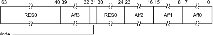
63 40 39 32 31 30 24 23 16 15 8 7 0
RES0 Aff3 RES0 Aff2 Aff1 Aff0
Interrupt_Routing_Mode
Bits [63:40]
Reserved, RES0.
Aff3, bits [39:32]
Affinity level 3, the least significant affinity level field.
On a Warm reset, this field resets to an architecturally UNKNOWN value.
Interrupt_Routing_Mode, bit [31]
Interrupt Routing Mode. Defines how SPIs are routed in an affinity hierarchy:
0b0 Interrupts routed to the PE specified by a.b.c.d. In this routing, a, b, c, and d are the values of fields Aff3, Aff2, Aff1, and Aff0 respectively.
0b1 Interrupts routed to any PE defined as a participating node.
If GICD_IROUTER
- The interrupt is not forwarded to any PE, direct reads return the written value
• The affinity path is treated as an UNKNOWN implemented PE, direct reads return the UNKNOWN implemented PE
- The affinity path is treated as an UNKNOWN implemented PE, direct reads return the written value
In implementations that do not require 1 of N distribution of SPIs, this bit might be RAZ/WI.
When this bit is set to 1, GICD_IROUTER
Note An implementation might choose to make the Aff
fields RO when this field is 1.
On a Warm reset, this field resets to an architecturally UNKNOWN value.
Bits [30:24]
Reserved, RES0.
Aff2, bits [23:16]
Affinity level 2, an intermediate affinity level field.
On a Warm reset, this field resets to an architecturally UNKNOWN value.
Aff1, bits [15:8]
Affinity level 1, an intermediate affinity level field.
On a Warm reset, this field resets to an architecturally UNKNOWN value.
Aff0, bits [7:0]
Affinity level 0, the most significant affinity level field.
On a Warm reset, this field resets to an architecturally UNKNOWN value.
For an SPI with INTID m:
-
The corresponding GICD_IROUTER
register number, n, is given by n = m. -
The offset of the GICD_IROUTER
register is 0x6000 + 8n.
Accessing the GICD_IROUTER:
These registers are used only when affinity routing is enabled. When affinity routing is not enabled:
-
These registers are RES0. An implementation is permitted to make the register RAZ/WI in this case.
-
The GICD_ITARGETSR
registers provide interrupt routing information.
Note
When affinity routing becomes enabled for a Security state (for example, following a reset or following a write to GICD_CTLR) the value of all writeable fields in this register is UNKNOWN for that Security state. When the group of an interrupt changes so the ARE setting for the interrupt changes to 1, the value of this register is UNKNOWN for that interrupt.
If GICD_CTLR.DS==0, unless the GICD_NSACR
Note For each interrupt, a GIC implementation might support fewer than 256 values for an affinity level. In this case, some bits of the corresponding affinity level field might be RO. Implementations must ensure that an interrupt that is pending at the time of the write uses either the old value or the new value and must ensure that the interrupt is neither lost nor handled more than one time. The effect of the change must be visible in finite time.
GICD_IROUTER
| Component | Offset | Instance |
|---|---|---|
| GIC Distributor | 0x6000+ (8 * n) | GICD_IROUTER |
This interface is accessible as follows:
-
When GICD_CTLR.DS == 0 accesses to this register are RW.
-
When an access is Secure accesses to this register are RW.
-
When an access is Non-secure accesses to this register are RW.
12.9.21 GICD_IROUTERE, Interrupt Routing Registers (Extended SPI Range), n = 0 - 1023
The GICD_IROUTER
Purpose
When affinity routing is enabled, provides routing information for the corresponding SPI in the extended SPI range.
Configurations
This register is present only when FEAT_GICv3p1 is implemented. Otherwise, direct accesses to GICD_IROUTER
RW fields in this register reset to architecturally UNKNOWN values.
When GICD_TYPER.ESPI==0, these registers are RES0. When GICD_TYPER.ESPI==1, the number of implemented GICD_IROUTER
Attributes
GICD_IROUTER
Field descriptions
The GICD_IROUTER
| 63 | 40 39 32 31 30 24 23 16 15 8 7 0 | 40 39 32 31 30 24 23 16 15 8 7 0 | 40 39 32 31 30 24 23 16 15 8 7 0 | 40 39 32 31 30 24 23 16 15 8 7 0 | 40 39 32 31 30 24 23 16 15 8 7 0 | 40 39 32 31 30 24 23 16 15 8 7 0 | 40 39 32 31 30 24 23 16 15 8 7 0 | 40 39 32 31 30 24 23 16 15 8 7 0 |
|---|---|---|---|---|---|---|---|---|
| d | RES0 | Aff3 | RES0 | Aff2 | Aff1 | Aff0 |
Interrupt_Routing_Mode
Bits [63:40]
Reserved, RES0.
Aff3, bits [39:32]
Affinity level 3, the least significant affinity level field. Interrupt_Routing_Mode, bit [31] Interrupt Routing Mode. Defines how SPIs are routed in an affinity hierarchy: 0b0 Interrupts routed to the PE specified by a.b.c.d. In this routing, a, b, c, and d are the values of fields Aff3, Aff2, Aff1, and Aff0 respectively. 0b1 Interrupts routed to any PE defined as a participating node. If GICD_IROUTER
Note An implementation might choose to make the Aff
fields RO when this field is 1.
Bits [30:24]
Reserved, RES0.
Aff2, bits [23:16]
Affinity level 2, an intermediate affinity level field.
Aff1, bits [15:8]
Affinity level 1, an intermediate affinity level field.
Aff0, bits [7:0]
Affinity level 0, the most significant affinity level field.
For an SPI with INTID m:
-
The corresponding GICD_IROUTER
E register number, n, is given by n = m. -
The offset of the GICD_IROUTER
E register is 0x6000 + 8n.
Accessing the GICD_IROUTERE:
When affinity routing is not enabled for the Security state of an interrupt in GICD_IROUTER
When GICD_CTLR.DS==0, a register that corresponds to a Group 0 or Secure Group 1 interrupt is RAZ/WI to Non-secure accesses.
Bits corresponding to unimplemented interrupts are RAZ/WI.
GICD_IROUTER
Component Offset Instance GIC Distributor 0x8000 + (8 * n) GICD_IROUTER
This interface is accessible as follows:
-
When GICD_CTLR.DS == 0 accesses to this register are RW.
-
When an access is Secure accesses to this register are RW.
-
When an access is Non-secure accesses to this register are RW.
12.9.22 GICD_ISACTIVER, Interrupt Set-Active Registers, n = 0 - 31
The GICD_ISACTIVER
Purpose
Activates the corresponding interrupt. These registers are used when saving and restoring GIC state.
Configurations
These registers are available in all GIC configurations. If GICD_CTLR.DS==0, these registers are Common.
The number of implemented GICD_ISACTIVER
(GICD_TYPER.ITLinesNumber+1). Registers are numbered from 0.
GICD_ISACTIVER0 is Banked for each connected PE with GICR_TYPER.Processor_Number < 8.
Accessing GICD_ISACTIVER0 from a PE with GICR_TYPER.Processor_Number > 7 is
CONSTRAINED UNPREDICTABLE:
-
Register is RAZ/WI.
-
An UNKNOWN banked copy of the register is accessed.
Attributes
GICD_ISACTIVER
Field descriptions
The GICD_ISACTIVER

Image text
31 30 29 28 27 26 25 24 23 22 21 20 19 18 17 16 15 14 13 12 11 10 9 8 7 6 5 4 3 2 1 0
Set_active_bit29 Set_active_bit2
Set_active_bit30 Set_active_bit3
Set_active_bit31 Set_active_bit4
Set_active_bit28 Set_active_bit5
Set_active_bit27 Set_active_bit6
Set_active_bit26 Set_active_bit7
Set_active_bit25 Set_active_bit8
Set_active_bit24 Set_active_bit9
Set_active_bit23 Set_active_bit10
Set_active_bit22 Set_active_bit11
Set_active_bit21 Set_active_bit12
Set_active_bit20 Set_active_bit13
Set_active_bit19 Set_active_bit14
Set_active_bit18 Set_active_bit15
Set_active_bit17
Set_active_bit16
Set_active_bit1
Set_active_bit0
0b0 If read, indicates that the corresponding interrupt is not active, and is not active and pending.
If written, has no effect. 0b1 If read, indicates that the corresponding interrupt is active, or is active and pending. If written, activates the corresponding interrupt, if the interrupt is not already active. If the interrupt is already active, the write has no effect. After a write of 1 to this bit, a subsequent read of this bit returns 1.
On a Warm reset, this field resets to 0.
For INTID m, when DIV and MOD are the integer division and modulo operations:
-
The corresponding GICD_ISACTIVER
number, n, is given by n = m DIV 32. -
The offset of the required GICD_ISACTIVER is (0x300 + (4*n)).
-
The bit number of the required group modifier bit in this register is m MOD 32.
Accessing the GICD_ISACTIVER:
When affinity routing is enabled for the Security state of an interrupt, bits corresponding to SGIs and PPIs are RAZ/WI, and equivalent functionality for SGIs and PPIs is provided by GICR_ISACTIVER0.
Bits corresponding to unimplemented interrupts are RAZ/WI.
If GICD_CTLR.DS==0, unless the GICD_NSACR
The bit reads as one if the status of the interrupt is active or active and pending. GICD_ISPENDR
GICD_ISACTIVER
Component Offset Instance GIC Distributor 0x0300 + (4 * n) GICD_ISACTIVER
This interface is accessible as follows:
-
When GICD_CTLR.DS == 0 accesses to this register are RW.
-
When an access is Secure accesses to this register are RW.
-
When an access is Non-secure accesses to this register are RW.
12.9.23 GICD_ISACTIVERE, Interrupt Set-Active Registers (extended SPI range), n = 0 - 31
The GICD_ISACTIVER
Purpose
Adds the active state to the corresponding SPI in the extended SPI range.
Configurations
This register is present only when FEAT_GICv3p1 is implemented. Otherwise, direct accesses to GICD_ISACTIVER
When GICD_TYPER.ESPI==0, these registers are RES0.
When GICD_TYPER.ESPI==1, the number of implemented GICD_ISACTIVER
Attributes
GICD_ISACTIVER
Field descriptions
The GICD_ISACTIVER
| 31 30 29 28 27 26 25 24 23 22 21 20 19 18 17 16 15 14 13 12 11 10 Set_active_bit29 Set_active_bit30 Set_active_bit31 Set_active_bit28 Set_active_bit27 Set_active_bit26 Set_active_bit25 Set_active_bit24 Set_active_bit23 Set_active_bit22 Set_active_bit21 Set_active_bit20 Set_active_bit19 Set_active_bit18 Set_active_bit17 Set_active_bit16 Set_active_bit1 Set_active_bit0 | 31 30 29 28 27 26 25 24 23 22 21 20 19 18 17 16 15 14 13 12 11 10 Set_active_bit29 Set_active_bit30 Set_active_bit31 Set_active_bit28 Set_active_bit27 Set_active_bit26 Set_active_bit25 Set_active_bit24 Set_active_bit23 Set_active_bit22 Set_active_bit21 Set_active_bit20 Set_active_bit19 Set_active_bit18 Set_active_bit17 Set_active_bit16 Set_active_bit1 Set_active_bit0 | 31 30 29 28 27 26 25 24 23 22 21 20 19 18 17 16 15 14 13 12 11 10 Set_active_bit29 Set_active_bit30 Set_active_bit31 Set_active_bit28 Set_active_bit27 Set_active_bit26 Set_active_bit25 Set_active_bit24 Set_active_bit23 Set_active_bit22 Set_active_bit21 Set_active_bit20 Set_active_bit19 Set_active_bit18 Set_active_bit17 Set_active_bit16 Set_active_bit1 Set_active_bit0 | 31 30 29 28 27 26 25 24 23 22 21 20 19 18 17 16 15 14 13 12 11 10 Set_active_bit29 Set_active_bit30 Set_active_bit31 Set_active_bit28 Set_active_bit27 Set_active_bit26 Set_active_bit25 Set_active_bit24 Set_active_bit23 Set_active_bit22 Set_active_bit21 Set_active_bit20 Set_active_bit19 Set_active_bit18 Set_active_bit17 Set_active_bit16 Set_active_bit1 Set_active_bit0 | 31 30 29 28 27 26 25 24 23 22 21 20 19 18 17 16 15 14 13 12 11 10 Set_active_bit29 Set_active_bit30 Set_active_bit31 Set_active_bit28 Set_active_bit27 Set_active_bit26 Set_active_bit25 Set_active_bit24 Set_active_bit23 Set_active_bit22 Set_active_bit21 Set_active_bit20 Set_active_bit19 Set_active_bit18 Set_active_bit17 Set_active_bit16 Set_active_bit1 Set_active_bit0 | 31 30 29 28 27 26 25 24 23 22 21 20 19 18 17 16 15 14 13 12 11 10 Set_active_bit29 Set_active_bit30 Set_active_bit31 Set_active_bit28 Set_active_bit27 Set_active_bit26 Set_active_bit25 Set_active_bit24 Set_active_bit23 Set_active_bit22 Set_active_bit21 Set_active_bit20 Set_active_bit19 Set_active_bit18 Set_active_bit17 Set_active_bit16 Set_active_bit1 Set_active_bit0 | 31 30 29 28 27 26 25 24 23 22 21 20 19 18 17 16 15 14 13 12 11 10 Set_active_bit29 Set_active_bit30 Set_active_bit31 Set_active_bit28 Set_active_bit27 Set_active_bit26 Set_active_bit25 Set_active_bit24 Set_active_bit23 Set_active_bit22 Set_active_bit21 Set_active_bit20 Set_active_bit19 Set_active_bit18 Set_active_bit17 Set_active_bit16 Set_active_bit1 Set_active_bit0 | 31 30 29 28 27 26 25 24 23 22 21 20 19 18 17 16 15 14 13 12 11 10 Set_active_bit29 Set_active_bit30 Set_active_bit31 Set_active_bit28 Set_active_bit27 Set_active_bit26 Set_active_bit25 Set_active_bit24 Set_active_bit23 Set_active_bit22 Set_active_bit21 Set_active_bit20 Set_active_bit19 Set_active_bit18 Set_active_bit17 Set_active_bit16 Set_active_bit1 Set_active_bit0 | 31 30 29 28 27 26 25 24 23 22 21 20 19 18 17 16 15 14 13 12 11 10 Set_active_bit29 Set_active_bit30 Set_active_bit31 Set_active_bit28 Set_active_bit27 Set_active_bit26 Set_active_bit25 Set_active_bit24 Set_active_bit23 Set_active_bit22 Set_active_bit21 Set_active_bit20 Set_active_bit19 Set_active_bit18 Set_active_bit17 Set_active_bit16 Set_active_bit1 Set_active_bit0 | 31 30 29 28 27 26 25 24 23 22 21 20 19 18 17 16 15 14 13 12 11 10 Set_active_bit29 Set_active_bit30 Set_active_bit31 Set_active_bit28 Set_active_bit27 Set_active_bit26 Set_active_bit25 Set_active_bit24 Set_active_bit23 Set_active_bit22 Set_active_bit21 Set_active_bit20 Set_active_bit19 Set_active_bit18 Set_active_bit17 Set_active_bit16 Set_active_bit1 Set_active_bit0 | 31 30 29 28 27 26 25 24 23 22 21 20 19 18 17 16 15 14 13 12 11 10 Set_active_bit29 Set_active_bit30 Set_active_bit31 Set_active_bit28 Set_active_bit27 Set_active_bit26 Set_active_bit25 Set_active_bit24 Set_active_bit23 Set_active_bit22 Set_active_bit21 Set_active_bit20 Set_active_bit19 Set_active_bit18 Set_active_bit17 Set_active_bit16 Set_active_bit1 Set_active_bit0 | 31 30 29 28 27 26 25 24 23 22 21 20 19 18 17 16 15 14 13 12 11 10 Set_active_bit29 Set_active_bit30 Set_active_bit31 Set_active_bit28 Set_active_bit27 Set_active_bit26 Set_active_bit25 Set_active_bit24 Set_active_bit23 Set_active_bit22 Set_active_bit21 Set_active_bit20 Set_active_bit19 Set_active_bit18 Set_active_bit17 Set_active_bit16 Set_active_bit1 Set_active_bit0 | 31 30 29 28 27 26 25 24 23 22 21 20 19 18 17 16 15 14 13 12 11 10 Set_active_bit29 Set_active_bit30 Set_active_bit31 Set_active_bit28 Set_active_bit27 Set_active_bit26 Set_active_bit25 Set_active_bit24 Set_active_bit23 Set_active_bit22 Set_active_bit21 Set_active_bit20 Set_active_bit19 Set_active_bit18 Set_active_bit17 Set_active_bit16 Set_active_bit1 Set_active_bit0 | 31 30 29 28 27 26 25 24 23 22 21 20 19 18 17 16 15 14 13 12 11 10 Set_active_bit29 Set_active_bit30 Set_active_bit31 Set_active_bit28 Set_active_bit27 Set_active_bit26 Set_active_bit25 Set_active_bit24 Set_active_bit23 Set_active_bit22 Set_active_bit21 Set_active_bit20 Set_active_bit19 Set_active_bit18 Set_active_bit17 Set_active_bit16 Set_active_bit1 Set_active_bit0 | 31 30 29 28 27 26 25 24 23 22 21 20 19 18 17 16 15 14 13 12 11 10 Set_active_bit29 Set_active_bit30 Set_active_bit31 Set_active_bit28 Set_active_bit27 Set_active_bit26 Set_active_bit25 Set_active_bit24 Set_active_bit23 Set_active_bit22 Set_active_bit21 Set_active_bit20 Set_active_bit19 Set_active_bit18 Set_active_bit17 Set_active_bit16 Set_active_bit1 Set_active_bit0 | 31 30 29 28 27 26 25 24 23 22 21 20 19 18 17 16 15 14 13 12 11 10 Set_active_bit29 Set_active_bit30 Set_active_bit31 Set_active_bit28 Set_active_bit27 Set_active_bit26 Set_active_bit25 Set_active_bit24 Set_active_bit23 Set_active_bit22 Set_active_bit21 Set_active_bit20 Set_active_bit19 Set_active_bit18 Set_active_bit17 Set_active_bit16 Set_active_bit1 Set_active_bit0 | 31 30 29 28 27 26 25 24 23 22 21 20 19 18 17 16 15 14 13 12 11 10 Set_active_bit29 Set_active_bit30 Set_active_bit31 Set_active_bit28 Set_active_bit27 Set_active_bit26 Set_active_bit25 Set_active_bit24 Set_active_bit23 Set_active_bit22 Set_active_bit21 Set_active_bit20 Set_active_bit19 Set_active_bit18 Set_active_bit17 Set_active_bit16 Set_active_bit1 Set_active_bit0 | 31 30 29 28 27 26 25 24 23 22 21 20 19 18 17 16 15 14 13 12 11 10 Set_active_bit29 Set_active_bit30 Set_active_bit31 Set_active_bit28 Set_active_bit27 Set_active_bit26 Set_active_bit25 Set_active_bit24 Set_active_bit23 Set_active_bit22 Set_active_bit21 Set_active_bit20 Set_active_bit19 Set_active_bit18 Set_active_bit17 Set_active_bit16 Set_active_bit1 Set_active_bit0 | 31 30 29 28 27 26 25 24 23 22 21 20 19 18 17 16 15 14 13 12 11 10 Set_active_bit29 Set_active_bit30 Set_active_bit31 Set_active_bit28 Set_active_bit27 Set_active_bit26 Set_active_bit25 Set_active_bit24 Set_active_bit23 Set_active_bit22 Set_active_bit21 Set_active_bit20 Set_active_bit19 Set_active_bit18 Set_active_bit17 Set_active_bit16 Set_active_bit1 Set_active_bit0 | 31 30 29 28 27 26 25 24 23 22 21 20 19 18 17 16 15 14 13 12 11 10 Set_active_bit29 Set_active_bit30 Set_active_bit31 Set_active_bit28 Set_active_bit27 Set_active_bit26 Set_active_bit25 Set_active_bit24 Set_active_bit23 Set_active_bit22 Set_active_bit21 Set_active_bit20 Set_active_bit19 Set_active_bit18 Set_active_bit17 Set_active_bit16 Set_active_bit1 Set_active_bit0 | 31 30 29 28 27 26 25 24 23 22 21 20 19 18 17 16 15 14 13 12 11 10 Set_active_bit29 Set_active_bit30 Set_active_bit31 Set_active_bit28 Set_active_bit27 Set_active_bit26 Set_active_bit25 Set_active_bit24 Set_active_bit23 Set_active_bit22 Set_active_bit21 Set_active_bit20 Set_active_bit19 Set_active_bit18 Set_active_bit17 Set_active_bit16 Set_active_bit1 Set_active_bit0 | 31 30 29 28 27 26 25 24 23 22 21 20 19 18 17 16 15 14 13 12 11 10 Set_active_bit29 Set_active_bit30 Set_active_bit31 Set_active_bit28 Set_active_bit27 Set_active_bit26 Set_active_bit25 Set_active_bit24 Set_active_bit23 Set_active_bit22 Set_active_bit21 Set_active_bit20 Set_active_bit19 Set_active_bit18 Set_active_bit17 Set_active_bit16 Set_active_bit1 Set_active_bit0 | 31 30 29 28 27 26 25 24 23 22 21 20 19 18 17 16 15 14 13 12 11 10 Set_active_bit29 Set_active_bit30 Set_active_bit31 Set_active_bit28 Set_active_bit27 Set_active_bit26 Set_active_bit25 Set_active_bit24 Set_active_bit23 Set_active_bit22 Set_active_bit21 Set_active_bit20 Set_active_bit19 Set_active_bit18 Set_active_bit17 Set_active_bit16 Set_active_bit1 Set_active_bit0 | 31 30 29 28 27 26 25 24 23 22 21 20 19 18 17 16 15 14 13 12 11 10 Set_active_bit29 Set_active_bit30 Set_active_bit31 Set_active_bit28 Set_active_bit27 Set_active_bit26 Set_active_bit25 Set_active_bit24 Set_active_bit23 Set_active_bit22 Set_active_bit21 Set_active_bit20 Set_active_bit19 Set_active_bit18 Set_active_bit17 Set_active_bit16 Set_active_bit1 Set_active_bit0 | 31 30 29 28 27 26 25 24 23 22 21 20 19 18 17 16 15 14 13 12 11 10 Set_active_bit29 Set_active_bit30 Set_active_bit31 Set_active_bit28 Set_active_bit27 Set_active_bit26 Set_active_bit25 Set_active_bit24 Set_active_bit23 Set_active_bit22 Set_active_bit21 Set_active_bit20 Set_active_bit19 Set_active_bit18 Set_active_bit17 Set_active_bit16 Set_active_bit1 Set_active_bit0 | 31 30 29 28 27 26 25 24 23 22 21 20 19 18 17 16 15 14 13 12 11 10 Set_active_bit29 Set_active_bit30 Set_active_bit31 Set_active_bit28 Set_active_bit27 Set_active_bit26 Set_active_bit25 Set_active_bit24 Set_active_bit23 Set_active_bit22 Set_active_bit21 Set_active_bit20 Set_active_bit19 Set_active_bit18 Set_active_bit17 Set_active_bit16 Set_active_bit1 Set_active_bit0 | 31 30 29 28 27 26 25 24 23 22 21 20 19 18 17 16 15 14 13 12 11 10 Set_active_bit29 Set_active_bit30 Set_active_bit31 Set_active_bit28 Set_active_bit27 Set_active_bit26 Set_active_bit25 Set_active_bit24 Set_active_bit23 Set_active_bit22 Set_active_bit21 Set_active_bit20 Set_active_bit19 Set_active_bit18 Set_active_bit17 Set_active_bit16 Set_active_bit1 Set_active_bit0 | 31 30 29 28 27 26 25 24 23 22 21 20 19 18 17 16 15 14 13 12 11 10 Set_active_bit29 Set_active_bit30 Set_active_bit31 Set_active_bit28 Set_active_bit27 Set_active_bit26 Set_active_bit25 Set_active_bit24 Set_active_bit23 Set_active_bit22 Set_active_bit21 Set_active_bit20 Set_active_bit19 Set_active_bit18 Set_active_bit17 Set_active_bit16 Set_active_bit1 Set_active_bit0 | 31 30 29 28 27 26 25 24 23 22 21 20 19 18 17 16 15 14 13 12 11 10 Set_active_bit29 Set_active_bit30 Set_active_bit31 Set_active_bit28 Set_active_bit27 Set_active_bit26 Set_active_bit25 Set_active_bit24 Set_active_bit23 Set_active_bit22 Set_active_bit21 Set_active_bit20 Set_active_bit19 Set_active_bit18 Set_active_bit17 Set_active_bit16 Set_active_bit1 Set_active_bit0 | 31 30 29 28 27 26 25 24 23 22 21 20 19 18 17 16 15 14 13 12 11 10 Set_active_bit29 Set_active_bit30 Set_active_bit31 Set_active_bit28 Set_active_bit27 Set_active_bit26 Set_active_bit25 Set_active_bit24 Set_active_bit23 Set_active_bit22 Set_active_bit21 Set_active_bit20 Set_active_bit19 Set_active_bit18 Set_active_bit17 Set_active_bit16 Set_active_bit1 Set_active_bit0 | 31 30 29 28 27 26 25 24 23 22 21 20 19 18 17 16 15 14 13 12 11 10 Set_active_bit29 Set_active_bit30 Set_active_bit31 Set_active_bit28 Set_active_bit27 Set_active_bit26 Set_active_bit25 Set_active_bit24 Set_active_bit23 Set_active_bit22 Set_active_bit21 Set_active_bit20 Set_active_bit19 Set_active_bit18 Set_active_bit17 Set_active_bit16 Set_active_bit1 Set_active_bit0 | 9 8 7 6 5 | 9 8 7 6 5 | 9 8 7 6 5 | 9 8 7 6 5 | 9 8 7 6 5 | 9 8 7 6 5 | 9 8 7 6 5 | 9 8 7 6 5 | 9 8 7 6 5 | 9 8 7 6 5 | 4 3 2 1 0 Set_active_bit2 Set_active_bit3 Set_active_bit4 Set_active_bit5 Set_active_bit6 Set_active_bit7 Set_active_bit8 Set_active_bit9 Set_active_bit10 Set_active_bit11 Set_active_bit12 Set_active_bit13 Set_active_bit14 Set_active_bit15 | 4 3 2 1 0 Set_active_bit2 Set_active_bit3 Set_active_bit4 Set_active_bit5 Set_active_bit6 Set_active_bit7 Set_active_bit8 Set_active_bit9 Set_active_bit10 Set_active_bit11 Set_active_bit12 Set_active_bit13 Set_active_bit14 Set_active_bit15 | 4 3 2 1 0 Set_active_bit2 Set_active_bit3 Set_active_bit4 Set_active_bit5 Set_active_bit6 Set_active_bit7 Set_active_bit8 Set_active_bit9 Set_active_bit10 Set_active_bit11 Set_active_bit12 Set_active_bit13 Set_active_bit14 Set_active_bit15 | 4 3 2 1 0 Set_active_bit2 Set_active_bit3 Set_active_bit4 Set_active_bit5 Set_active_bit6 Set_active_bit7 Set_active_bit8 Set_active_bit9 Set_active_bit10 Set_active_bit11 Set_active_bit12 Set_active_bit13 Set_active_bit14 Set_active_bit15 | 4 3 2 1 0 Set_active_bit2 Set_active_bit3 Set_active_bit4 Set_active_bit5 Set_active_bit6 Set_active_bit7 Set_active_bit8 Set_active_bit9 Set_active_bit10 Set_active_bit11 Set_active_bit12 Set_active_bit13 Set_active_bit14 Set_active_bit15 | 4 3 2 1 0 Set_active_bit2 Set_active_bit3 Set_active_bit4 Set_active_bit5 Set_active_bit6 Set_active_bit7 Set_active_bit8 Set_active_bit9 Set_active_bit10 Set_active_bit11 Set_active_bit12 Set_active_bit13 Set_active_bit14 Set_active_bit15 |
|---|---|---|---|---|---|---|---|---|---|---|---|---|---|---|---|---|---|---|---|---|---|---|---|---|---|---|---|---|---|---|---|---|---|---|---|---|---|---|---|---|---|---|---|---|---|---|
| bit29 bit30 bit31 bit28 bit27 bit26 bit25 bit24 bit23 bit22 bit21 bit20 bit19 bit18 bit17 bit16 bit1 i | S S S S S S S S Set Set Set Set Set Set | a a a a a a a a ti ti ti ti ti ti | ||||||||||||||||||||||||||||||||||||||||||||
Set_active_bit, bit [x], for x = 31 to 0
For the extended SPIs, adds the active state to interrupt number x. Reads and writes have the following behavior:
- 0b0 If read, indicates that the corresponding interrupt is not active, and is not active and pending.
If written, has no effect.
- 0b1 If read, indicates that the corresponding interrupt is active, or active and pending on this PE.
If written, activates the corresponding interrupt, if the interrupt is not already active. If the interrupt is already active, the write has no effect. After a write of 1 to this bit, a subsequent read of this bit returns 1.
On a Warm reset, this field resets to 0.
For INTID m, when DIV and MOD are the integer division and modulo operations:
-
The corresponding GICD_ISACTIVER
E number, n, is given by n = (m-4096) DIV 32. -
The offset of the required GICD_ISACTIVER
E is (0x1A00 + (4*n)). -
The bit number of the required group modifier bit in this register is (m-4096) MOD 32.
Accessing the GICD_ISACTIVERE:
When affinity routing is not enabled for the Security state of an interrupt in GICD_ISACTIVER
When GICD_CTLR.DS==0, bits corresponding to Secure SPIs are RAZ/WI to Non-secure accesses.
Bits corresponding to unimplemented interrupts are RAZ/WI.
GICD_ISACTIVER
| Component | Offset | Instance |
|---|---|---|
| GIC Distributor | 0x1A00+ (4 * n) | GICD_ISACTIVER |
This interface is accessible as follows:
-
When GICD_CTLR.DS == 0 accesses to this register are RW.
-
When an access is Secure accesses to this register are RW.
-
When an access is Non-secure accesses to this register are RW.
12.9.24 GICD_ISENABLER, Interrupt Set-Enable Registers, n = 0 - 31
The GICD_ISENABLER
Purpose
Enables forwarding of the corresponding interrupt to the CPU interfaces.
Configurations
These registers are available in all GIC configurations. If GICD_CTLR.DS==0, these registers are Common.
The number of implemented GICD_ISENABLER
(GICD_TYPER.ITLinesNumber+1). Registers are numbered from 0.
GICD_ISENABLER0 is Banked for each connected PE with GICR_TYPER.Processor_Number < 8.
Accessing GICD_ISENABLER0 from a PE with GICR_TYPER.Processor_Number > 7 is
CONSTRAINED UNPREDICTABLE:
-
Register is RAZ/WI.
-
An UNKNOWN banked copy of the register is accessed.
Attributes
GICD_ISENABLER
Field descriptions
The GICD_ISENABLER

Image text
31 30 29 28 27 26 25 24 23 22 21 20 19 18 17 16 15 14 13 12 11 10 9 8 7 6 5 4 3 2 1 0
Set_enable_bit29 Set_enable_bit2
Set_enable_bit30 Set_enable_bit3
Set_enable_bit31 Set_enable_bit4
Set_enable_bit28 Set_enable_bit5
Set_enable_bit27 Set_enable_bit6
Set_enable_bit26 Set_enable_bit7
Set_enable_bit25 Set_enable_bit8
Set_enable_bit24 Set_enable_bit9
Set_enable_bit23 Set_enable_bit10
Set_enable_bit22 Set_enable_bit11
Set_enable_bit21 Set_enable_bit12
Set_enable_bit20 Set_enable_bit13
Set_enable_bit19 Set_enable_bit14
Set_enable_bit18 Set_enable_bit15
Set_enable_bit17
Set_enable_bit16
Set_enable_bit1
Set_enable_bit0
0b0 If read, indicates that forwarding of the corresponding interrupt is disabled. If written, has no effect. 0b1 If read, indicates that forwarding of the corresponding interrupt is enabled. If written, enables forwarding of the corresponding interrupt. After a write of 1 to this bit, a subsequent read of this bit returns 1.
For SGIs, the behavior of this bit is IMPLEMENTATION DEFINED. On a Warm reset, this field resets to an architecturally UNKNOWN value.
For INTID m, when DIV and MOD are the integer division and modulo operations:
-
The corresponding GICD_ISENABLER
number, n, is given by n = m DIV 32. -
The offset of the required GICD_ISENABLER is (0x100 + (4*n)).
-
The bit number of the required group modifier bit in this register is m MOD 32.
At start-up, and after a reset, a PE can use this register to discover which peripheral INTIDs the GIC supports. If GICD_CTLR.DS==0 in a system that supports EL3, the PE must do this for the Secure view of the available interrupts, and Non-secure software running on the PE must do this discovery after the Secure software has configured interrupts as Group 0/Secure Group 1 and Non-secure Group 1.
Accessing the GICD_ISENABLER:
For SGIs and PPIs:
-
When ARE is 1 for the Security state of an interrupt, the field for that interrupt is RES0 and an implementation is permitted to make the field RAZ/WI in this case.
-
Equivalent functionality is provided by GICR_ISENABLER0.
Bits corresponding to unimplemented interrupts are RAZ/WI.
When GICD_CTLR.DS==0, bits corresponding to Group 0 or Secure Group 1 interrupts are RAZ/WI to Non-secure accesses.
It is IMPLEMENTATION DEFINED whether implemented SGIs are permanently enabled, or can be enabled and disabled by writes to GICD_ISENABLER
For SPIs and PPIs, each bit controls the forwarding of the corresponding interrupt from the Distributor to the CPU interfaces.
GICD_ISENABLER
Component Offset Instance GIC Distributor 0x0100 + (4 * n) GICD_ISENABLER
This interface is accessible as follows:
-
When GICD_CTLR.DS == 0 accesses to this register are RW.
-
When an access is Secure accesses to this register are RW.
-
When an access is Non-secure accesses to this register are RW.
12.9.25 GICD_ISENABLERE, Interrupt Set-Enable Registers, n = 0 - 31
The GICD_ISENABLER
Purpose
Enables forwarding of the corresponding SPI in the extended SPI range to the CPU interfaces.
Configurations
This register is present only when FEAT_GICv3p1 is implemented. Otherwise, direct accesses to GICD_ISENABLER
When GICD_TYPER.ESPI==0, these registers are RES0.
When GICD_TYPER.ESPI==1, the number of implemented GICD_ISENABLER
Attributes
GICD_ISENABLER
Field descriptions
The GICD_ISENABLER
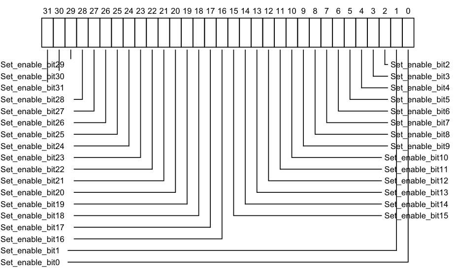
Image text
31 30 29 28 27 26 25 24 23 22 21 20 19 18 17 16 15 14 13 12 11 10 9 8 7 6 5 4 3 2 1 0
Set_enable_bit29 Set_enable_bit2
Set_enable_bit30 Set_enable_bit3
Set_enable_bit31 Set_enable_bit4
Set_enable_bit28 Set_enable_bit5
Set_enable_bit27 Set_enable_bit6
Set_enable_bit26 Set_enable_bit7
Set_enable_bit25 Set_enable_bit8
Set_enable_bit24 Set_enable_bit9
Set_enable_bit23 Set_enable_bit10
Set_enable_bit22 Set_enable_bit11
Set_enable_bit21 Set_enable_bit12
Set_enable_bit20 Set_enable_bit13
Set_enable_bit19 Set_enable_bit14
Set_enable_bit18 Set_enable_bit15
Set_enable_bit17
Set_enable_bit16
Set_enable_bit1
Set_enable_bit0
-
0b0 If read, indicates that forwarding of the corresponding interrupt is disabled. If written, has no effect.
-
0b1 If read, indicates that forwarding of the corresponding interrupt is enabled. If written, enables forwarding of the corresponding interrupt. After a write of 1 to this bit, a subsequent read of this bit returns 1.
-
On a Warm reset, this field resets to 0. For INTID m, when DIV and MOD are the integer division and modulo operations:
-
The corresponding GICD_ISENABLER
E number, n, is given by n = (m-4096) DIV 32. -
The offset of the required GICD_ISENABLER
E is (0x1200 + (4*n)). -
The bit number of the required group modifier bit in this register is (m-4096) MOD 32.
Accessing the GICD_ISENABLERE:
When affinity routing is not enabled for the Security state of an interrupt in GICD_ISENABLER
When GICD_CTLR.DS==0, bits corresponding to Secure SPIs are RAZ/WI to Non-secure accesses.
Bits corresponding to unimplemented interrupts are RAZ/WI.
GICD_ISENABLER
Component Offset Instance
GIC Distributor 0x1200 + (4 * n) GICD_ISENABLER
This interface is accessible as follows:
-
When GICD_CTLR.DS == 0 accesses to this register are RW.
-
When an access is Secure accesses to this register are RW.
-
When an access is Non-secure accesses to this register are RW.
12.9.26 GICD_ISPENDR, Interrupt Set-Pending Registers, n = 0 - 31
The GICD_ISPENDR
Purpose
Adds the pending state to the corresponding interrupt.
Configurations
These registers are available in all GIC configurations. If GICD_CTLR.DS==0, these registers are Common.
The number of implemented GICD_ISPENDR
(GICD_TYPER.ITLinesNumber+1). Registers are numbered from 0.
GICD_ISPENDR0 is Banked for each connected PE with GICR_TYPER.Processor_Number < 8.
Accessing GICD_ISPENDR0 from a PE with GICR_TYPER.Processor_Number > 7 is
CONSTRAINED UNPREDICTABLE:
-
Register is RAZ/WI.
-
An UNKNOWN banked copy of the register is accessed.
Attributes
GICD_ISPENDR
Field descriptions
The GICD_ISPENDR
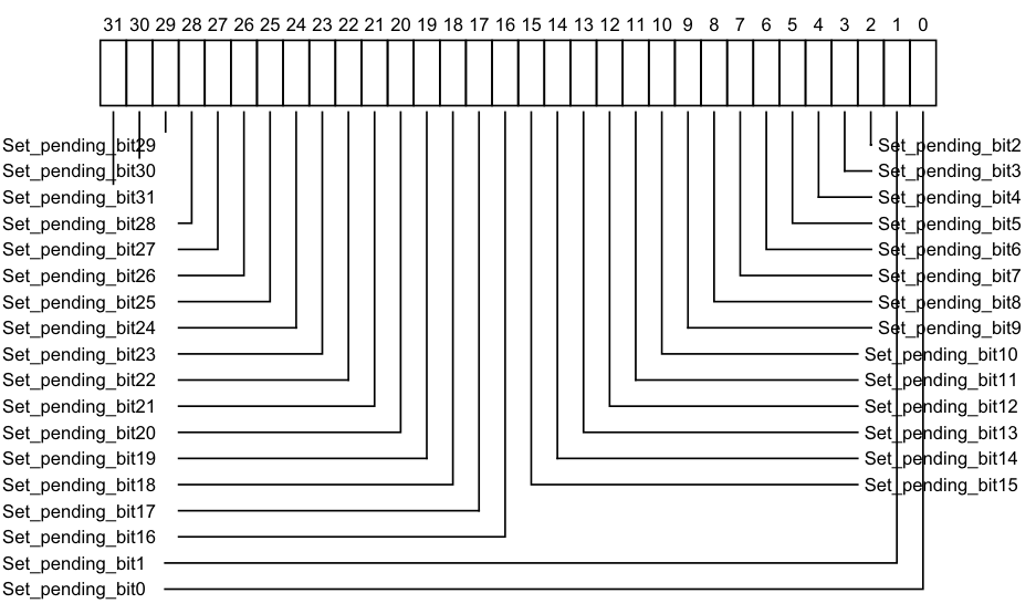
Image text
31 30 29 28 27 26 25 24 23 22 21 20 19 18 17 16 15 14 13 12 11 10 9 8 7 6 5 4 3 2 1 0
Set_pending_bit29 Set_pending_bit2
Set_pending_bit30 Set_pending_bit3
Set_pending_bit31 Set_pending_bit4
Set_pending_bit28 Set_pending_bit5
Set_pending_bit27 Set_pending_bit6
Set_pending_bit26 Set_pending_bit7
Set_pending_bit25 Set_pending_bit8
Set_pending_bit24 Set_pending_bit9
Set_pending_bit23 Set_pending_bit10
Set_pending_bit22 Set_pending_bit11
Set_pending_bit21 Set_pending_bit12
Set_pending_bit20 Set_pending_bit13
Set_pending_bit19 Set_pending_bit14
Set_pending_bit18 Set_pending_bit15
Set_pending_bit17
Set_pending_bit16
Set_pending_bit1
Set_pending_bit0
0b0 If read, indicates that the corresponding interrupt is not pending on any PE. If written, has no effect.
- 0b1
If read, indicates that the corresponding interrupt is pending, or active and pending:
-
On this PE if the interrupt is an SGI or PPI.
-
On at least one PE if the interrupt is an SPI.
-
If written, changes the state of the corresponding interrupt from inactive to pending, or from active to active and pending. This has no effect in the following cases:
-
If the interrupt is an SGI. The pending state of an SGI can be set using GICD_SPENDSGIR
. -
If the interrupt is not inactive and is not active.
-
If the interrupt is already pending because of a write to GICD_ISPENDR
. -
If the interrupt is already pending because the corresponding interrupt signal is asserted. In this case, the interrupt remains pending if the interrupt signal is deasserted.
On a Warm reset, this field resets to 0.
Accessing the GICD_ISPENDR:
Set-pending bits for SGIs are read-only and ignore writes. The Set-pending bits for SGIs are provided as GICD_SPENDSGIR
When affinity routing is enabled for the Security state of an interrupt:
-
Bits corresponding to SGIs and PPIs are RAZ/WI, and equivalent functionality for SGIs and PPIs is provided by GICR_ISPENDR0.
-
Bits corresponding to Group 0 and Group 1 Secure interrupts can only be set by Secure accesses.
Bits corresponding to unimplemented interrupts are RAZ/WI.
If GICD_CTLR.DS==0, unless the GICD_NSACR
GICD_ISPENDR
| Component | Offset | Instance |
|---|---|---|
| GIC Distributor | 0x0200+ (4 * n) | GICD_ISPENDR |
This interface is accessible as follows:
-
When GICD_CTLR.DS == 0 accesses to this register are RW.
-
When an access is Secure accesses to this register are RW.
-
When an access is Non-secure accesses to this register are RW.
12.9.27 GICD_ISPENDRE, Interrupt Set-Pending Registers (extended SPI range), n = 0 - 31
The GICD_ISPENDR
Purpose
Adds the pending state to the corresponding SPI in the extended SPI range.
Configurations
This register is present only when FEAT_GICv3p1 is implemented. Otherwise, direct accesses to GICD_ISPENDR
When GICD_TYPER.ESPI==0, these registers are RES0.
When GICD_TYPER.ESPI==1, the number of implemented GICD_ISPENDR
Attributes
GICD_ISPENDR
Field descriptions
The GICD_ISPENDR
31 30 29 28 27 26 25 24 23 22 21 20 19 18 17 16 15 14 13 12 11 10 9 8 7 6 5 4 3 2 1 0 Set_pending_bit29 Set_pending_bit2 Set_pending_bit30 Set_pending_bit3 Set_pending_bit31 Set_pending_bit4 Set_pending_bit28 Set_pending_bit5 Set_pending_bit27 Set_pending_bit6 Set_pending_bit26 Set_pending_bit7 Set_pending_bit25 Set_pending_bit8 Set_pending_bit24 Set_pending_bit9 Set_pending_bit23 Set_pending_bit10 Set_pending_bit22 Set_pending_bit11 Set_pending_bit21 Set_pending_bit12 Set_pending_bit20 Set_pending_bit13 Set_pending_bit19 Set_pending_bit14 Set_pending_bit18 Set_pending_bit15 Set_pending_bit17 Set_pending_bit16 Set_pending_bit1 Set_pending_bit0
Set_pending_bit, bit [x], for x = 31 to 0
For the extended SPIs, adds the pending state to interrupt number x. Reads and writes have the following behavior:
-
0b0 If read, indicates that the corresponding interrupt is not pending. If written, has no effect.
-
0b1 If read, indicates that the corresponding interrupt is pending, or active and pending. If written, changes the state of the corresponding interrupt from inactive to pending, or from active to active and pending.
-
This has no effect in the following cases:
-
If the interrupt is already pending because of a write to GICD_ISPENDR
E.
-
-
If the interrupt is already pending because the corresponding interrupt signal is asserted. In this case, the interrupt remains pending if the interrupt signal is deasserted.
On a Warm reset, this field resets to 0.
For INTID m, when DIV and MOD are the integer division and modulo operations:
-
The corresponding GICD_ISPENDR
E number, n, is given by n = (m-4096) DIV 32. -
The offset of the required GICD_ISPENDR
E is (0x1600 + (4*n)). -
The bit number of the required group modifier bit in this register is (m-4096) MOD 32.
Accessing the GICD_ISPENDRE:
When affinity routing is not enabled for the Security state of an interrupt in GICD_ISPENDR
When GICD_CTLR.DS==0, bits corresponding to Secure SPIs are RAZ/WI to Non-secure accesses.
Bits corresponding to unimplemented interrupts are RAZ/WI.
GICD_ISPENDR
Component Offset Instance GIC Distributor 0x1600 + (4 * n) GICD_ISPENDR
This interface is accessible as follows:
-
When GICD_CTLR.DS == 0 accesses to this register are RW.
-
When an access is Secure accesses to this register are RW.
-
When an access is Non-secure accesses to this register are RW.
12.9.28 GICD_ITARGETSR, Interrupt Processor Targets Registers, n = 0 - 254
The GICD_ITARGETSR
Purpose
When affinity routing is not enabled, holds the list of target PEs for the interrupt. That is, it holds the list of CPU interfaces to which the Distributor forwards the interrupt if it is asserted and has sufficient priority.
Configurations
These registers are available in all configurations of the GIC. When GICD_CTLR.DS==0, these registers are Common.
The number of implemented GICD_ITARGETSR
8*(GICD_TYPER.ITLinesNumber+1). Registers are numbered from 0.
GICD_ITARGETSR0 to GICD_ITARGETSR7 are Banked for each connected PEwith GICR_TYPER.Processor_Number < 8.
Accessing GICD_ITARGETSR0 to GICD_ITARGETSR7 from a PE with
GICR_TYPER.Processor_Number > 7 is CONSTRAINED UNPREDICTABLE:
-
Register is RAZ/WI.
-
An UNKNOWN banked copy of the register is accessed.
Attributes
GICD_ITARGETSR
Field descriptions
The GICD_ITARGETSR
| | 31 | 24 | 23 | 16 | 15 | 8 | 7 | 0 | | |—|— CPU_targets_offset_3B |—|— CPU_targets_offset_2B |—|— CPU_targets_offset_1B |—|— CPU_targets_offset_0B |—|—| |||||||||||
PEs in the system number from 0, and each bit in a PE targets field refers to the corresponding PE. For example, a value of 0x3 means that the Pending interrupt is sent to PEs 0 and 1. For
GICD_ITARGETSR0-GICD_ITARGETSR7, a read of any targets field returns the number of the PE performing the read.
CPU_targets_offset_3B, bits [31:24]
PE targets for an interrupt, at byte offset 3.
On a Warm reset, this field resets to an architecturally UNKNOWN value.
CPU_targets_offset_2B, bits [23:16]
PE targets for an interrupt, at byte offset 2.
On a Warm reset, this field resets to an architecturally UNKNOWN value.
CPU_targets_offset_1B, bits [15:8]
PE targets for an interrupt, at byte offset 1.
On a Warm reset, this field resets to an architecturally UNKNOWN value.
CPU_targets_offset_0B, bits [7:0]
PE targets for an interrupt, at byte offset 0.
On a Warm reset, this field resets to an architecturally UNKNOWN value. The bits that are set to 1 in the PE targets field determine which PEs are targeted:
| Value of PE targets field | Interrupt targets |
|---|---|
| 0bxxxxxxx1 | CPU interface 0 |
| 0bxxxxxx1x | CPU interface 1 |
| 0bxxxxx1xx | CPU interface 2 |
| 0bxxxx1xxx | CPU interface 3 |
| 0bxxx1xxxx | CPU interface 4 |
| 0bxx1xxxxx | CPU interface 5 |
| 0bx1xxxxxx | CPU interface 6 |
| 0b1xxxxxxx | CPU interface 7 |
For interrupt ID m, when DIV and MOD are the integer division and modulo operations:
-
The corresponding GICD_ITARGETSR
number, n, is given by n = m DIV 4. -
The offset of the required GICD_ITARGETSR
register is (0x800 + (4*n)). -
The byte offset of the required Priority field in this register is m MOD 4, where:
-
Byte offset 0 refers to register bits [7:0].
-
Byte offset 1 refers to register bits [15:8].
-
Byte offset 2 refers to register bits [23:16].
-
Byte offset 3 refers to register bits [31:24].
-
Software can write to these registers at any time. Any change to a targets field value:
-
Has no effect on any active interrupt. This means that removing a CPU interface from a targets list does not cancel an active state for interrupts on that CPU interface. There is no effect on interrupts that are active and pending until the active status is cleared, at which time it is treated as a pending interrupt.
-
Has an effect on any pending interrupts. This means:
-
Enables the CPU interface to be chosen as a target for the pending interrupt using an IMPLEMENTATION DEFINED mechanism.
-
Removing a CPU interface from the target list of a pending interrupt removes the pending state of the interrupt on that CPU interface.
-
Accessing the GICD_ITARGETSR:
These registers are used when affinity routing is not enabled. When affinity routing is enabled for the Security state of an interrupt, the target PEs for an interrupt are defined by GICD_IROUTER
-
These registers are byte-accessible.
-
A register field corresponding to an unimplemented interrupt is RAZ/WI.
-
A field bit corresponding to an unimplemented CPU interface is RAZ/WI.
-
GICD_ITARGETSR0-GICD_ITARGETSR7 are read-only. Each field returns a value that corresponds only to the PE reading the register.
-
It is IMPLEMENTATION DEFINED which, if any, SPIs are statically configured in hardware. The field for such an SPI is read-only, and returns a value that indicates the PE targets for the interrupt.
-
If GICD_CTLR.DS==0, unless the GICD_NSACR
registers permit Non-secure software to control Group 0 and Secure Group 1 interrupts, any bits that correspond to Group 0 or Secure Group 1 interrupts are accessible only by Secure accesses and are RAZ/WI to Non-secure accesses.
In a single connected PE implementation, all interrupts target one PE, and these registers are RAZ/WI.
Note Implementations must ensure that an interrupt that is pending at the time of the write uses either the old value or the new value and must ensure that the interrupt is neither lost nor handled more than one time. The effect of the change must be visible in finite time.
GICD_ITARGETSR
Component Offset Instance GIC Distributor 0x0800 + (4 * n) GICD_ITARGETSR
This interface is accessible as follows:
-
When GICD_CTLR.DS == 0 accesses to this register are RW.
-
When an access is Secure accesses to this register are RW.
-
When an access is Non-secure accesses to this register are RW.
12.9.29 GICD_NSACR, Non-secure Access Control Registers, n = 0 - 63
The GICD_NSACR
Purpose
Enables Secure software to permit Non-secure software on a particular PE to create and control Group 0 interrupts.
Configurations
The concept of selective enabling of Non-secure access to Group 0 and Secure Group 1 interrupts applies to SGIs and SPIs.
GICD_NSACR0 is a Banked register used for SGIs. A copy is provided for every PE that has a CPU interface and that supports this feature.
Attributes
GICD_NSACR
Field descriptions
The GICD_NSACR
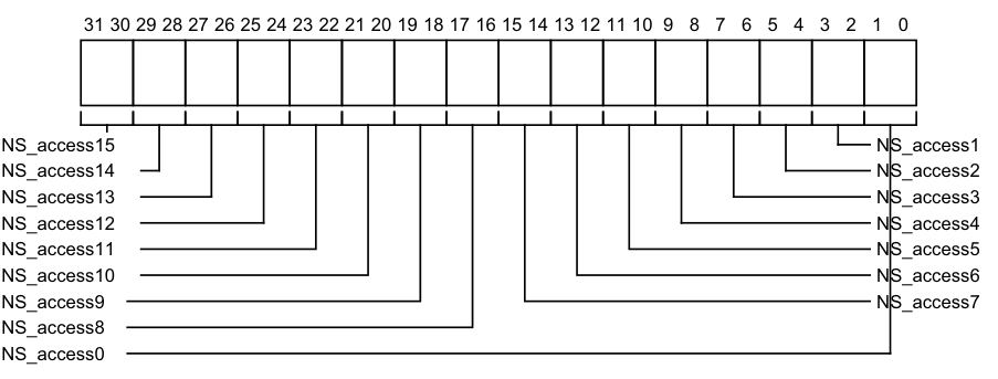
Image text
31 30 29 28 27 26 25 24 23 22 21 20 19 18 17 16 15 14 13 12 11 10 9 8 7 6 5 4 3 2 1 0
NS_access15 NS_access1
NS_access14 NS_access2
NS_access13 NS_access3
NS_access12 NS_access4
NS_access11 NS_access5
NS_access10 NS_access6
NS_access9 NS_access7
NS_access8
NS_access0
If the corresponding interrupt does not support configurable Non-secure access, the field is RAZ/WI.
Otherwise, the field is RW and determines the level of Non-secure control permitted if the interrupt is a Secure interrupt. If the interrupt is a Non-secure interrupt, this field is ignored. The possible values of each 2-bit field are:
0b00 No Non-secure access is permitted to fields associated with the corresponding interrupt. 0b01 Non-secure read and write access is permitted to set-pending bits in GICD_ISPENDR
An implementation might also provide read access to clear-pending bits in GICD_ICPENDR
0b10 As 0b01, but adds Non-secure read and write access permission to fields associated with the corresponding interrupt in the GICD_ICPENDR
0b11 For GICD_NSACR0 this encoding is reserved and treated as 10. For all other GICD_NSACR
On a Warm reset, this field resets to 0.
For interrupt ID m, when DIV and MOD are the integer division and modulo operations:
-
The corresponding GICD_NSACR
number, n, is given by n = m DIV 16. -
The offset of the required GICD_NSACR
register is (0xE00 + (4*n)).
Note Because each field in this register comprises two bits, GICD_NSACR0 controls access rights to SGI registers, GICD_NSACR1 controls access to PPI registers (and is always RAZ/WI), and all other GICD_NSACR
registers control access to SPI registers.
For compatibility with GICv2, writes to GICD_NSACR0 for a particular PE must be coordinated within the Distributor and must update GICR_NSACR for the Redistributor associated with that PE.
Accessing the GICD_NSACR:
These registers are always used when affinity routing is not enabled. When affinity routing is enabled for the Secure state, GICD_NSACR0 is RES0 and GICR_NSACR provides equivalent functionality for SGIs.
These registers do not support PPIs, therefore GICD_NSACR1 is RAZ/WI.
GICD_NSACR
Component Offset Instance GIC Distributor 0x0E00 + (4 * n) GICD_NSACR
This interface is accessible as follows:
-
When GICD_CTLR.DS == 1 accesses to this register are RAZ/WI.
-
When an access is Secure accesses to this register are RW.
-
When an access is Non-secure accesses to this register are RAZ/WI.
12.9.30 GICD_NSACRE, Non-secure Access Control Registers, n = 0 - 63
The GICD_NSACR
Purpose
Enables Secure software to permit Non-secure software on a particular PE to create and control Group 0 interrupts.
Configurations
This register is present only when FEAT_GICv3p1 is implemented. Otherwise, direct accesses to GICD_NSACR
When GICD_TYPER.ESPI==0, these registers are RES0.
When GICD_TYPER.ESPI==1, the number of implemented GICD_ICFGR
Attributes
GICD_NSACR
Field descriptions
The GICD_NSACR

Image text
31 30 29 28 27 26 25 24 23 22 21 20 19 18 17 16 15 14 13 12 11 10 9 8 7 6 5 4 3 2 1 0
NS_access15 NS_access1
NS_access14 NS_access2
NS_access13 NS_access3
NS_access12 NS_access4
NS_access11 NS_access5
NS_access10 NS_access6
NS_access9 NS_access7
NS_access8
NS_access0
If the corresponding interrupt does not support configurable Non-secure access, the field is RAZ/WI.
Otherwise, the field is RW and determines the level of Non-secure control permitted if the interrupt is a Secure interrupt. If the interrupt is a Non-secure interrupt, this field is ignored. The possible values of each 2-bit field are:
0b00 No Non-secure access is permitted to fields associated with the corresponding interrupt. 0b01 Non-secure read and write access is permitted to set-pending bits in GICD_ISPENDR
0b11
This encoding is treated as 0b10, but adds Non-secure read and write access permission to GICD_IROUTER
On a Warm reset, this field resets to 0.
For interrupt ID m, when DIV and MOD are the integer division and modulo operations:
-
The corresponding GICD_NSACR
E number, n, is given by n = (m - 4096) DIV 16. -
The offset of the required GICD_NSACR
E register is (0x3600 + (4*n)).
Accessing the GICD_NSACRE:
GICD_NSACR
Component Offset Instance GIC Distributor 0x3600 + (4 * n) GICD_NSACR
This interface is accessible as follows:
-
When GICD_CTLR.DS == 1 accesses to this register are RAZ/WI.
-
When an access is Secure accesses to this register are RW.
-
When an access is Non-secure accesses to this register are RAZ/WI.
12.9.31 GICD_SETSPI_NSR, Set Non-secure SPI Pending Register
The GICD_SETSPI_NSR characteristics are:
Purpose
Adds the pending state to a valid SPI if permitted by the Security state of the access and the GICD_NSACR
A write to this register changes the state of an inactive SPI to pending, and the state of an active SPI to active and pending.
Configurations
If GICD_TYPER.MBIS == 0, this register is reserved.
When GICD_CTLR.DS==1, this register provides functionality for all SPIs.
Attributes
GICD_SETSPI_NSR is a 32-bit register.
Field descriptions
The GICD_SETSPI_NSR bit assignments are:

31 13 12 0
RES0 INTID
Bits [31:13]
Reserved, RES0.
INTID, bits [12:0]
The INTID of the SPI.
The function of this register depends on whether the targeted SPI is configured to be an edge-triggered or level-sensitive interrupt:
-
For an edge-triggered interrupt, a write to GICD_SETSPI_NSR or GICD_SETSPI_SR adds the pending state to the targeted interrupt. It will stop being pending on activation, or if the pending state is removed by a write to GICD_CLRSPI_NSR, GICD_CLRSPI_SR, or GICD_ICPENDR
. -
For a level-sensitive interrupt, a write to GICD_SETSPI_NSR or GICD_SETSPI_SR adds the pending state to the targeted interrupt. It will remain pending until it is deasserted by a write to GICD_CLRSPI_NSR or GICD_CLRSPI_SR. If the interrupt is activated between having the pending state added and being deactivated, then the interrupt will be active and pending.
Accessing the GICD_SETSPI_NSR:
Writes to this register have no effect if:
-
The value written specifies a Secure SPI, the value is written by a Non-secure access, and the value of the corresponding GICD_NSACR
register is 0. -
The value written specifies an invalid SPI.
-
The SPI is already pending.
-
16-bit accesses to bits [15:0] of this register must be supported.
Note A Secure access to this register can set the pending state of any valid SPI.
GICD_SETSPI_NSR can be accessed through its memory-mapped interface:
| Component | Offset | Instance |
|---|---|---|
| GIC Distributor | 0x0040 | GICD_SETSPI_NSR |
This interface is accessible as follows:
-
When GICD_CTLR.DS == 0 accesses to this register are WO.
-
When an access is Secure accesses to this register are WO.
-
When an access is Non-secure accesses to this register are WO.
12.9.32 GICD_SETSPI_SR, Set Secure SPI Pending Register
The GICD_SETSPI_SR characteristics are:
Purpose
Adds the pending state to a valid SPI.
A write to this register changes the state of an inactive SPI to pending, and the state of an active SPI to active and pending.
Configurations
If GICD_TYPER.MBIS == 0, this register is reserved.
When GICD_CTLR.DS==1, this register is WI.
Attributes
GICD_SETSPI_SR is a 32-bit register.
Field descriptions
The GICD_SETSPI_SR bit assignments are:

31 13 12 0
RES0 INTID
Bits [31:13]
Reserved, RES0.
INTID, bits [12:0]
The INTID of the SPI.
The function of this register depends on whether the targeted SPI is configured to be an edge-triggered or level-sensitive interrupt:
-
For an edge-triggered interrupt, a write to GICD_SETSPI_NSR or GICD_SETSPI_SR adds the pending state to the targeted interrupt. It will stop being pending on activation, or if the pending state is removed by a write to GICD_CLRSPI_NSR, GICD_CLRSPI_SR, or GICD_ICPENDR
. -
For a level-sensitive interrupt, a write to GICD_SETSPI_NSR or GICD_SETSPI_SR adds the pending state to the targeted interrupt. It will remain pending until it is deasserted by a write to GICD_CLRSPI_NSR or GICD_CLRSPI_SR. If the interrupt is activated between having the pending state added and being deactivated, then the interrupt will be active and pending.
Accessing the GICD_SETSPI_SR:
Writes to this register have no effect if:
-
The value is written by a Non-secure access.
-
The value written specifies an invalid SPI.
-
The SPI is already pending.
16-bit accesses to bits [15:0] of this register must be supported. GICD_SETSPI_SR can be accessed through its memory-mapped interface:
| Component | Offset | Instance |
|---|---|---|
| GIC Distributor | 0x0050 | GICD_SETSPI_SR |
This interface is accessible as follows:
-
When GICD_CTLR.DS == 0 accesses to this register are WI.
-
When an access is Secure accesses to this register are WO.
-
When an access is Non-secure accesses to this register are WI.
12.9.33 GICD_SGIR, Software Generated Interrupt Register
The GICD_SGIR characteristics are:
Purpose
Controls the generation of SGIs.
Configurations
This register is available in all configurations of the GIC. If the GIC supports two Security states this register is Common.
Attributes
GICD_SGIR is a 32-bit register.
Field descriptions
The GICD_SGIR bit assignments are:
| TargetListFilter | RES0 31 26 25 24 CPUTargetList 23 16 15 RES0 14 4 INTID 3 0 NSATT | RES0 31 26 25 24 CPUTargetList 23 16 15 RES0 14 4 INTID 3 0 NSATT | RES0 31 26 25 24 CPUTargetList 23 16 15 RES0 14 4 INTID 3 0 NSATT | RES0 31 26 25 24 CPUTargetList 23 16 15 RES0 14 4 INTID 3 0 NSATT | RES0 31 26 25 24 CPUTargetList 23 16 15 RES0 14 4 INTID 3 0 NSATT | RES0 31 26 25 24 CPUTargetList 23 16 15 RES0 14 4 INTID 3 0 NSATT | RES0 31 26 25 24 CPUTargetList 23 16 15 RES0 14 4 INTID 3 0 NSATT | RES0 31 26 25 24 CPUTargetList 23 16 15 RES0 14 4 INTID 3 0 NSATT | |—|— RES0 |— RES0 |—|— CPUTargetList |—|— RES0 INTID |— RES0 |— INTID | |||||||||| |||||||||| ||||||||||
Bits [31:26]
Reserved, RES0.
TargetListFilter, bits [25:24]
Determines how the Distributor processes the requested SGI.
0b00 Forward the interrupt to the CPU interfaces specified by GICD_SGIR.CPUTargetList. 0b01 Forward the interrupt to all CPU interfaces except that of the PE that requested the interrupt. 0b10 Forward the interrupt only to the CPU interface of the PE that requested the interrupt. 0b11 Reserved.
CPUTargetList, bits [23:16]
When GICD_SGIR.TargetListFilter is 0b00, this field defines the CPU interfaces to which the Distributor must forward the interrupt.
Each bit of the field refers to the corresponding CPU interface. For example, CPUTargetList[0] corresponds to interface 0. Setting a bit to 1 indicates that the interrupt must be forwarded to the corresponding interface.
If this field is 0b00000000 when GICD_SGIR.TargetListFilter is 0b00, the Distributor does not forward the interrupt to any CPU interface.
NSATT, bit [15]
Specifies the required group of the SGI.
0b0 Forward the SGI specified in the INTID field to a specified CPU interface only if the SGI is configured as Group 0 on that interface. 0b1 Forward the SGI specified in the INTID field to a specified CPU interface only if the SGI is configured as Group 1 on that interface. This field is writable only by a Secure access. Non-secure accesses can also generate Group 0 interrupts, if allowed to do so by GICD_NSACR0. Otherwise, Non-secure writes to GICD_SGIR generate an SGI only if the specified SGI is programmed as Group 1, regardless of the value of bit [15] of the write.
Bits [14:4]
Reserved, RES0.
INTID, bits [3:0]
The INTID of the SGI to forward to the specified CPU interfaces.
Accessing the GICD_SGIR:
This register is used only when affinity routing is not enabled. When affinity routing is enabled, this register is RES0.
It is IMPLEMENTATION DEFINED whether this register has any effect when the forwarding of interrupts by the Distributor is disabled by GICD_CTLR.
GICD_SGIR can be accessed through its memory-mapped interface:
| Component | Offset | Instance |
|---|---|---|
| GIC Distributor | 0x0F00 | GICD_SGIR |
This interface is accessible as follows:
-
When GICD_CTLR.DS == 0 accesses to this register are WO.
-
When an access is Secure accesses to this register are WO.
-
When an access is Non-secure accesses to this register are WO.
12.9.34 GICD_SPENDSGIR, SGI Set-Pending Registers, n = 0 - 3
The GICD_SPENDSGIR
Purpose
Adds the pending state to an SGI.
A write to this register changes the state of an inactive SGI to pending, and the state of an active SGI to active and pending.
Configurations
Four SGI set-pending registers are implemented. Each register contains eight set-pending bits for each of four SGIs, for a total of 16 possible SGIs.
In multiprocessor implementations, each PE has a copy of these registers.
Attributes
GICD_SPENDSGIR
Field descriptions
The GICD_SPENDSGIR
| | 31 | 24 | 23 | 16 | 15 | 8 | 7 | 0 | | |—|— SGI_set_pending_bits3 |—|— SGI_set_pending_bits2 |—|— SGI_set_pending_bits1 |—|— SGI_set_pending_bits0 |—|—| |||||||||||
SGI_set_pending_bits, bits [8x+7:8x], for x = 3 to 0
Adds the pending state to SGI number 4n + x for the PE corresponding to the bit number written to.
Reads and writes have the following behavior:
0x00 If read, indicates that the SGI from the corresponding PE is not pending and is not active and pending. If written, has no effect. 0x01 If read, indicates that the SGI from the corresponding PE is pending or is active and pending.
If written, adds the pending state to the SGI for the corresponding PE.
On a Warm reset, this field resets to 0.
For SGI ID m, generated by processing element C writing to the corresponding GICD_SGIR field, where DIV and MOD are the integer division and modulo operations:
-
The corresponding GICD_SPENDSGIR
number is given by n = m DIV 4. -
The offset of the required register is (0xF20 + (4n)).
-
The offset of the required field within the register GICD_SPENDSGIR
is given by m MOD 4. -
The required bit in the 8-bit SGI set-pending field m is bit C.
Accessing the GICD_SPENDSGIR:
These registers are used only when affinity routing is not enabled. When affinity routing is enabled for the Security state of an interrupt then the bit associated with SGI in that Security state is RES0. An implementation is permitted to make the register RAZ/WI in this case.
A register bit that corresponds to an unimplemented SGI is RAZ/WI.
These registers are byte-accessible. If the GIC implementation supports two Security states:
-
A register bit that corresponds to a Group 0 interrupt is RAZ/WI to Non-secure accesses.
-
Register bits corresponding to unimplemented PEs are RAZ/WI.
GICD_SPENDSGIR
| Component | Offset | Instance |
|---|---|---|
| GIC Distributor | 0x0F20+ (4 * n) | GICD_SPENDSGIR |
This interface is accessible as follows:
-
When GICD_CTLR.DS == 0 accesses to this register are RW.
-
When an access is Secure accesses to this register are RW.
-
When an access is Non-secure accesses to this register are RW.
12.9.35 GICD_STATUSR, Error Reporting Status Register
The GICD_STATUSR characteristics are:
Purpose
Provides software with a mechanism to detect:
-
Accesses to reserved locations.
-
Writes to read-only locations.
-
Reads of write-only locations.
Configurations
If the GIC implementation supports two Security states this register is Banked to provide Secure and Non-secure copies.
Attributes
GICD_STATUSR is a 32-bit register.
Field descriptions
The GICD_STATUSR bit assignments are:

Image text
31 4 3 2 1 0
RES0
RRD
WRD
RWOD
WROD
WROD, bit [3]
Write to an RO location. 0b0 Normal operation. 0b1 A write to an RO location has been detected. When a violation is detected, software must write 1 to this register to reset it.
RWOD, bit [2]
Read of a WO location. 0b0 Normal operation. 0b1 A read of a WO location has been detected. When a violation is detected, software must write 1 to this register to reset it.
WRD, bit [1]
Write to a reserved location.
0b0 Normal operation. 0b1 A write to a reserved location has been detected. When a violation is detected, software must write 1 to this register to reset it.
RRD, bit [0]
Read of a reserved location. 0b0 Normal operation. 0b1 A read of a reserved location has been detected. When a violation is detected, software must write 1 to this register to reset it.
Accessing the GICD_STATUSR:
This is an optional register. If the register is not implemented, the location is RAZ/WI.
GICD_STATUSR can be accessed through its memory-mapped interface:
Component Offset Instance GIC Distributor 0x0010 GICD_STATUSR (S)
This interface is accessible as follows:
-
When GICD_CTLR.DS == 0 accesses to this register are RW.
-
When an access is Secure accesses to this register are RW.
GICD_STATUSR can be accessed through its memory-mapped interface:
Component Offset Instance GIC Distributor 0x0010 GICD_STATUSR (NS)
This interface is accessible as follows:
-
When GICD_CTLR.DS == 0 accesses to this register are RW.
-
When an access is Non-secure accesses to this register are RW.
12.9.36 GICD_TYPER, Interrupt Controller Type Register
The GICD_TYPER characteristics are:
Purpose
Provides information about what features the GIC implementation supports. It indicates:
-
Whether the GIC implementation supports two Security states.
-
The maximum number of INTIDs that the GIC implementation supports.
-
The number of PEs that can be used as interrupt targets.
Configurations
This register is available in all configurations of the GIC. When GICD_CTLR.DS==0, this register is Common.
Attributes
GICD_TYPER is a 32-bit register.
Field descriptions
The GICD_TYPER bit assignments are:
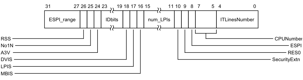
Image text
31 27 26 25 24 23 19 18 17 16 15 11 10 9 8 7 5 4 0
ESPI_range IDbits num_LPIs ITLinesNumber
RSS CPUNumber
No1N ESPI
A3V RES0
DVIS SecurityExtn
LPIS
MBIS
ESPI_range Indicates the maximum INTID in the Extended SPI range. Maximum Extended SPI INTID is (32*(ESPI_range + 1) + 4095)
Otherwise:
Reserved, RES0.
When GICD_TYPER.ESPI == 1:
ESPI_range Indicates the maximum INTID in the Extended SPI range. Maximum Extended SPI INTID is (32*(ESPI_range + 1) + 4095)
Otherwise:
Reserved, RES0.
RSS, bit [26]
Range Selector Support.
0b0 The IRI supports targeted SGIs with affinity level 0 values of 0 - 15. 0b1 The IRI supports targeted SGIs with affinity level 0 values of 0 - 255.
No1N, bit [25]
Indicates whether 1 of N SPI interrupts are supported. 0b0 1 of N SPI interrupts are supported. 0b1 1 of N SPI interrupts are not supported.
A3V, bit [24]
Affinity 3 valid. Indicates whether the Distributor supports nonzero values of Affinity level 3. 0b0 The Distributor only supports zero values of Affinity level 3. 0b1 The Distributor supports nonzero values of Affinity level 3.
IDbits, bits [23:19]
The number of interrupt identifier bits supported, minus one.
DVIS, bit [18]
When FEAT_GICv4 is implemented:
DVIS Indicates whether the implementation supports Direct Virtual LPI injection. 0b0 The implementation does not support Direct Virtual LPI injection. 0b1 The implementation supports Direct Virtual LPI injection.
Otherwise:
Reserved, RES0.
When FEAT_GICv4 is implemented:
DVIS Indicates whether the implementation supports Direct Virtual LPI injection. 0b0 The implementation does not support Direct Virtual LPI injection. 0b1 The implementation supports Direct Virtual LPI injection.
Otherwise:
Reserved, RES0.
LPIS, bit [17]
Indicates whether the implementation supports LPIs. 0b0 The implementation does not support LPIs. 0b1 The implementation supports LPIs.
MBIS, bit [16]
Indicates whether the implementation supports message-based interrupts by writing to Distributor registers. 0b0 The implementation does not support message-based interrupts by writing to Distributor registers. The GICD_CLRSPI_NSR, GICD_SETSPI_NSR, GICD_CLRSPI_SR, and GICD_SETSPI_SR registers are reserved. 0b1 The implementation supports message-based interrupts by writing to the GICD_CLRSPI_NSR, GICD_SETSPI_NSR, GICD_CLRSPI_SR, or GICD_SETSPI_SR registers.
num_LPIs, bits [15:11]
Number of supported LPIs.
-
0b00000 Number of LPIs as indicated by GICD_TYPER.IDbits.
-
All other values Number of LPIs supported is 2[(num_LPIs+1)] .
— Available LPI INTIDs are 8192..(8192 + 2[(num_LPIs+1)] - 1). — This field cannot indicate a maximum LPI INTID greater than that indicated by GICD_TYPER.IDbits.
When the supported INTID width is less than 14 bits, this field is RES0 and no LPIs are supported.
SecurityExtn, bit [10]
Indicates whether the GIC implementation supports two Security states:
When GICD_CTLR.DS == 1, this field is RAZ.
0b0 The GIC implementation supports only a single Security state.
0b1 The GIC implementation supports two Security states.
Bit [9]
Reserved, RES0.
ESPI, bit [8]
Extended SPI
0b0 Extended SPI range not implemented. 0b1 Extended SPI range implemented.
CPUNumber, bits [7:5]
Reports the number of PEs that can be used when affinity routing is not enabled, minus 1.
These PEs must be numbered contiguously from zero, but the relationship between this number and the affinity hierarchy from MPIDR is IMPLEMENTATION DEFINED. If the implementation does not support ARE being zero, this field is 000.
ITLinesNumber, bits [4:0]
For the INTID range 32 to 1019, indicates the maximum SPI supported.
If the value of this field is N, the maximum SPI INTID is 32(N+1) minus 1. For example, 00011 specifies that the maximum SPI INTID in is 127.
Regardless of the range of INTIDs defined by this field, interrupt IDs 1020-1023 are reserved for special purposes.
A value of 0 indicates no SPIs are support.
The ITLinesNumber field only indicates the maximum number of SPIs that the GIC implementation might support. This value determines the number of instances of the following interrupt registers:
-
GICD_IGROUPR
. -
GICD_ISENABLER
. -
GICD_ICENABLER
. -
GICD_ISPENDR
. -
GICD_ICPENDR
. -
GICD_ISACTIVER
. -
GICD_ICACTIVER
. -
GICD_IPRIORITYR
. -
GICD_ITARGETSR
. -
GICD_ICFGR
.
The GIC architecture does not require a GIC implementation to support a continuous range of SPI interrupt IDs. Software must check which SPI INTIDs are supported, up to the maximum value indicated by GICD_TYPER.ITLinesNumber.
Accessing the GICD_TYPER:
GICD_TYPER can be accessed through its memory-mapped interface:
| Component | Offset | Instance |
|---|---|---|
| GIC Distributor | 0x0004 | GICD_TYPER |
This interface is accessible as follows:
-
When GICD_CTLR.DS == 0 accesses to this register are RO.
-
When an access is Secure accesses to this register are RO.
-
When an access is Non-secure accesses to this register are RO.
12.9.37 GICD_TYPER2, Interrupt Controller Type Register 2
The GICD_TYPER2 characteristics are:
Purpose
Provides information about which features the GIC implementation supports.
Configurations
This register is present only when FEAT_GICv4p1 is implemented. Otherwise, direct accesses to GICD_TYPER2 are RES0.
When GICD_CTLR.DS == 0, this register is Common.
Attributes
GICD_TYPER2 is a 32-bit register.
Field descriptions
The GICD_TYPER2 bit assignments are:
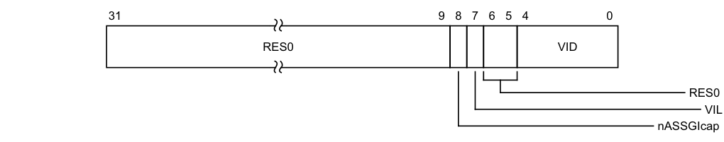
Image text
31 9 8 7 6 5 4 0
RES0 VID
RES0
VIL
nASSGIcap
nASSGIcap, bit [8]
Indicates whether SGIs can be configured to not have an active state.
0b0 SGIs have an active state.
0b1 SGIs can be globally configured not to have an active state.
This bit is RES0 on implementations that support two Security states.
VIL, bit [7]
Indicates whether 16 bits of vPEID are implemented.
0b0 GIC supports 16-bit vPEID. 0b1 GIC supports GICD_TYPER2.VID + 1 bits of vPEID.
Bits [6:5]
Reserved, RES0.
VID, bits [4:0]
When GICD_TYPER2.VIL == 1, the number of bits is equal to the bits of vPEID minus one. When GICD_TYPER2.VIL == 0, this field is RES0.
Accessing the GICD_TYPER2:
GICD_TYPER2 can be accessed through its memory-mapped interface:
| Component | Offset | Instance |
|---|---|---|
| GIC Distributor | 0x000C | GICD_TYPER2 |
This interface is accessible as follows:
-
When GICD_CTLR.DS == 0 accesses to this register are RO.
-
When an access is Secure accesses to this register are RO.
-
When an access is Non-secure accesses to this register are RO.
12.9.38 GICM_CLRSPI_NSR, Clear Non-secure SPI Pending Register
The GICM_CLRSPI_NSR characteristics are:
Purpose
Removes the pending state from a valid SPI if permitted by the Security state of the access and the GICD_NSACR
A write to this register changes the state of a pending SPI to inactive, and the state of an active and pending SPI to active.
Configurations
This register is present only when GICM_TYPER.CLR == 1. Otherwise, direct accesses to GICM_CLRSPI_NSR are RES0.
When GICD_CTLR.DS == 1, this register provides functionality for all SPIs.
Attributes
GICM_CLRSPI_NSR is a 32-bit register.
Field descriptions
The GICM_CLRSPI_NSR bit assignments are:

31 13 12 0
RES0 INTID
Bits [31:13]
Reserved, RES0.
INTID, bits [12:0]
This field is an alias of GICD_CLRSPI_NSR.
Accessing the GICM_CLRSPI_NSR:
Writes to this register have no effect if:
-
The value written specifies a Secure SPI, the value is written by a Non-secure access, and the value of the corresponding GICD_NSACR
register is less than 0b10. -
The value written specifies an invalid SPI.
-
The SPI is not pending.
16-bit accesses to bits [15:0] of this register must be supported.
Note A Secure access to this register can clear the pending state of any valid SPI.
GICM_CLRSPI_NSR can be accessed through its memory-mapped interface:
Component Frame Offset Instance GIC Distributor MSI_base 0x0048 GICM_CLRSPI_NSR This interface is accessible as follows:
-
When GICD_CTLR.DS == 0 accesses to this register are WO.
-
When an access is Secure accesses to this register are WO.
-
When an access is Non-secure accesses to this register are WO.
12.9.39 GICM_CLRSPI_SR, Clear Secure SPI Pending Register
The GICM_CLRSPI_SR characteristics are:
Purpose
Removes the pending state from a valid SPI.
A write to this register changes the state of a pending SPI to inactive, and the state of an active and pending SPI to active.
Configurations
This register is present only when GICM_TYPER.SR == 1 and GICM_TYPER.CLR == 1. Otherwise, direct accesses to GICM_CLRSPI_SR are RES0.
When GICD_CTLR.DS == 1, this register is WI.
Attributes
GICM_CLRSPI_SR is a 32-bit register.
Field descriptions
The GICM_CLRSPI_SR bit assignments are:

31 13 12 0
RES0 INTID
Bits [31:13]
Reserved, RES0.
INTID, bits [12:0]
This field is an alias of GICD_CLRSPI_SR.
Accessing the GICM_CLRSPI_SR:
Writes to this register have no effect if:
-
The value is written by a Non-secure access.
-
The value written specifies an invalid SPI.
-
The SPI is not pending.
16-bit accesses to bits [15:0] of this register must be supported.
GICM_CLRSPI_SR can be accessed through its memory-mapped interface:
| Component | Frame | Offset | Instance |
|---|---|---|---|
| GIC Distributor | MSI_base | 0x0058 | GICD_CLRSPI_SR |
This interface is accessible as follows:
-
When GICD_CTLR.DS == 0 accesses to this register are WI.
-
When an access is Secure accesses to this register are WO.
-
When an access is Non-secure accesses to this register are WI.
12.9.40 GICM_IIDR, Distributor Implementer Identification Register
The GICM_IIDR characteristics are:
Purpose
Provides information about the implementer and revision of the Distributor.
Configurations
This register is available in all configurations of the GIC. If the GIC implementation supports two Security states, this register is Common.
Attributes
GICM_IIDR is a 32-bit register.
Field descriptions
The GICM_IIDR bit assignments are:
| | 31 | | 24 | 23 | | 20 | 19 | | 16 | 15 | | 12 | 11 | | 0 | | |—|—|— ProductID |—|—|— RES0 |—|—|— Variant |—|—|— Revision |—|—|— Implementer |—|—| ||||||||||||||||||
ProductID, bits [31:24]
An IMPLEMENTATION DEFINED product identifier.
Bits [23:20]
Reserved, RES0.
Variant, bits [19:16]
An IMPLEMENTATION DEFINED variant number. Typically, this field is used to distinguish product variants, or major revisions of a product.
Revision, bits [15:12]
An IMPLEMENTATION DEFINED revision number. Typically, this field is used to distinguish minor revisions of a product.
Implementer, bits [11:0]
Contains the JEP106 code of the company that implemented the Distributor:
-
Bits [11:8] are the JEP106 continuation code of the implementer. For an Arm implementation, this field is 0x4.
-
Bit [7] is always 0.
-
Bits [6:0] are the JEP106 identity code of the implementer. For an Arm implementation, bits [7:0] are therefore 0x3B.
Accessing the GICM_IIDR:
GICM_IIDR can be accessed through its memory-mapped interface:
Component Frame Offset Instance
GIC Distributor MSI_base 0x0FCC GICM_IIDR This interface is accessible as follows:
-
When GICD_CTLR.DS == 0 accesses to this register are RO.
-
When an access is Secure accesses to this register are RO.
-
When an access is Non-secure accesses to this register are RO.
12.9.41 GICM_SETSPI_NSR, Set Non-secure SPI Pending Register
The GICM_SETSPI_NSR characteristics are:
Purpose
Adds the pending state to a valid SPI if permitted by the Security state of the access and the GICD_NSACR
A write to this register changes the state of an inactive SPI to pending, and the state of an active SPI to active and pending.
Configurations
When GICD_CTLR.DS==1, this register provides functionality for all SPIs.
Attributes
GICM_SETSPI_NSR is a 32-bit register.
Field descriptions
The GICM_SETSPI_NSR bit assignments are:

31 13 12 0
RES0 INTID
Bits [31:13]
Reserved, RES0.
INTID, bits [12:0]
This field is an alias of GICD_SETSPI_NSR.
Accessing the GICM_SETSPI_NSR:
Writes to this register have no effect if:
-
The value written specifies a Secure SPI, the value is written by a Non-secure access, and the value of the corresponding GICD_NSACR
register is 0. -
The value written specifies an invalid SPI.
-
The SPI is already pending.
-
16-bit accesses to bits [15:0] of this register must be supported.
Note A Secure access to this register can set the pending state of any valid SPI.
GICM_SETSPI_NSR can be accessed through its memory-mapped interface:
| Component | Frame | Offset | Instance |
|---|---|---|---|
| GIC Distributor | MSI_base | 0x0040 | GICM_SETSPI_NSR |
This interface is accessible as follows:
-
When GICD_CTLR.DS == 0 accesses to this register are WO.
-
When an access is Secure accesses to this register are WO.
-
When an access is Non-secure accesses to this register are WO.
12.9.42 GICM_SETSPI_SR, Set Secure SPI Pending Register
The GICM_SETSPI_SR characteristics are:
Purpose
Adds the pending state to a valid SPI.
A write to this register changes the state of an inactive SPI to pending, and the state of an active SPI to active and pending.
Configurations
This register is present only when GICM_TYPER.SR == 1. Otherwise, direct accesses to GICM_SETSPI_SR are RES0.
When GICD_CTLR.DS==1, this register is WI.
Attributes
GICM_SETSPI_SR is a 32-bit register.
Field descriptions
The GICM_SETSPI_SR bit assignments are:

31 13 12 0
RES0 INTID
Bits [31:13]
Reserved, RES0.
INTID, bits [12:0]
This field is an alias of GICD_SETSPI_SR.
Accessing the GICM_SETSPI_SR:
Writes to this register have no effect if:
-
The value is written by a Non-secure access.
-
The value written specifies an invalid SPI.
-
The SPI is already pending.
16-bit accesses to bits [15:0] of this register must be supported.
GICM_SETSPI_SR can be accessed through its memory-mapped interface:
| Component | Frame | Offset | Instance |
|---|---|---|---|
| GIC Distributor | MSI_base | 0x0050 | GICM_SETSPI_SR |
This interface is accessible as follows:
-
When GICD_CTLR.DS == 0 accesses to this register are WI.
-
When an access is Secure accesses to this register are WO.
-
When an access is Non-secure accesses to this register are WI.
12.9.43 GICM_TYPER, Distributor MSI Type Register
The GICM_TYPER characteristics are:
Purpose
Provides information about what features the GIC implementation supports.
Configurations
This register is available in all configurations of the GIC. When GICD_CTLR.DS==0, this register is Common.
Attributes
GICM_TYPER is a 32-bit register.
Field descriptions
The GICM_TYPER bit assignments are:
| Valid CLR | 31 30 SR 29 INTID 28 16 RES0 15 11 NumSPIs 10 0 |
|---|
Valid, bit [31]
Reports whether GICM_TYPER content is valid.
CLR, bit [30]
0b0 GICM_TYPER reports no information on the capabilities of the GICM frame, all other fields are RES0. 0b1 GICM_TYPER reports information on capabilities of GICM frame. Reports whether MSI clear registers are supported. 0b0 MSI clear registers not implemented. 0b1 MSI clear registers implemented.
SR, bit [29]
Reports whether Secure aliases of MSI registers are supported.
0b0 Secure aliases of MSI registers not implemented. 0b1 Secure aliases of MSI registers implemented.
INTID, bits [28:16]
INTID of the first SPI assigned to this GICM frame.
Bits [15:11]
Reserved, RES0.
NumSPIs, bits [10:0]
Number of SPIs assigned to this GICM frame.
Accessing the GICM_TYPER:
GICM_TYPER can be accessed through its memory-mapped interface:
| Component | Frame | Offset | Instance |
|---|---|---|---|
| GIC Distributor | MSI_base | 0x0004 | GICM_TYPER |
This interface is accessible as follows:
-
When GICD_CTLR.DS == 0 accesses to this register are RO.
-
When an access is Secure accesses to this register are RO.
-
When an access is Non-secure accesses to this register are RO.
12.10 The GIC Redistributor register map
This section describes the Redistributor register map.
The mechanism by which an ITS communicates with the Redistributors is IMPLEMENTATION DEFINED. An implementation might perform this communication using memory-mapped functionality, and a portion of the Redistributor memory map is allocated for such communication. The definition of the communication is outside the scope of this GIC architecture specification.
Each Redistributor defines two 64KB frames in the physical address map:
-
RD_base for controlling the overall behavior of the Redistributor, for controlling LPIs, and for generating LPIs in a system that does not include at least one ITS.
-
SGI_base for controlling and generating PPIs and SGIs.
The frame for each Redistributor must be contiguous and must be ordered as follows:
-
RD_base
-
SGI_base
In GICv4, there are two additional 64KB frames:
-
A frame to control virtual LPIs. The base address of this frame is referred to as VLPI_base.
-
A frame for a reserved page.
The frames for each Redistributor must be contiguous and must be ordered as follows:
-
RD_base
-
SGI_base
-
VLPI_base
-
Reserved
Reserved register addresses are RES0.
Table 12-27 shows the GIC Redistributor register map for the physical LPI registers.
Table 12-27 GIC physical LPI Redistributor register map
| Offset from RD_base | Name | Type | Reset | Description |
|---|---|---|---|---|
| 0x0000 | GICR_CTLR | RW | See the register description | Redistributor Control Register |
| 0x0004 | GICR_IIDR | RO | IMPLEMENTATION DEFINED | Implementer Identification Register |
| 0x0008 | GICR_TYPER | RO | IMPLEMENTATION DEFINED | Redistributor Type Register |
| 0x0010 | GICR_STATUSR | RW | 0x0000 0000 | Error Reporting Status Register, optional |
| 0x0014 | GICR_WAKER | RW | See the register description | Redistributor Wake Register |
| 0x0018 | GICR_MPAMIDR | RO | - | Report maximum PARTID and PMG Register |
| 0x001C | GICR_PARTIDR | RW | 0 | Set PARTID and PMG Register |
| 0x0020 | - | - | IMPLEMENTATION DEFINED | IMPLEMENTATION DEFINEDregisters |
| 0x0040 | GICR_SETLPIRa | WO | - | Set LPI Pending Register |
| 0x0048 | GICR_CLRLPIRa | WO | - | Clear LPI Pending Register |
| 0x0050 | - | - | - | Reserved |
| 0x0070 | GICR_PROPBASER | RW | - | Redistributor Properties Base Address Register |
| 0x0078 | GICR_PENDBASER | RW | - | Redistributor LPI Pending Table Base Address Register |
| Table 12-27 GIC physical LPI Redistributor register map (continued) |
| Offset from RD_base | Name | Type | Reset | Description |
|---|---|---|---|---|
| 0x00A0 | GICR_INVLPIRa | WO | - | Redistributor Invalidate LPI Register |
| 0x00A8 | - | - | - | Reserved |
| 0x00B0 | GICR_INVALLRa | WO | - | Redistributor Invalidate All Register |
| 0x00C0 | GICR_SYNCRa | RO | - | Redistributor Synchronize Register |
| 0x00C8 | - | - | - | Reserved |
| 0x0100 | - | WO | IMPLEMENTATION DEFINED | IMPLEMENTATION DEFINEDregisters |
| 0x0108 | - | - | - | Reserved |
| 0x0110 | - | WO | IMPLEMENTATION DEFINED | IMPLEMENTATION DEFINEDregisters |
| 0x0118-0xBFFC | - | - | - | Reserved |
| 0xC000-0xFFCC | - | - | IMPLEMENTATION DEFINED | IMPLEMENTATION DEFINEDregisters |
| 0xFFD0-0xFFFC | - | RO | IMPLEMENTATION DEFINED | Reserved for ID registers, see_Identification_ _registers_on page 12-205 |
- a. This register is mandatory in an implementation that supports LPIs and does not include an ITS, and when GICv4.1 is implemented. Otherwise, support for this register is IMPLEMENTATION DEFINED.
Table 12-28 shows the GIC Redistributor register map for the virtual LPI registers.
Table 12-28 GIC virtual LPI Redistributor register map
| Offset from VLPI_base | Name | Type | Reset | Description |
|---|---|---|---|---|
| 0x0000 | - | - | - | Reserved |
| 0x0040 | - | WO | IMPLEMENTATION DEFINED | IMPLEMENTATION DEFINEDregisters |
| 0x0050 | - | - | - | Reserved |
| 0x0070 | GICR_VPROPBASER | RW | - | Virtual Redistributor Properties Base Address Register |
| 0x0078 | GICR_VPENDBASER | RW | - | Virtual Pending Table Base Address Register |
| 0x0080 | GICR_VSGIR | WO | - | Redistributor virtual SGI pending state request register |
| 0x0088 | GICR_VSGIPENDR | RO | - | Redistributor virtual SGI pending state register |
| 0x0080-0x037C | - | RW | IMPLEMENTATION DEFINED | IMPLEMENTATION DEFINEDregisters |
| 0x0380-0xBFFC | - | - | - | Reserved |
| 0xC000-0xFFCC | - | - | IMPLEMENTATION DEFINED | IMPLEMENTATION DEFINEDregisters |
| 0xFFD0-0xFFFC | - | - | - | Reserved |
Table 12-29 shows the GIC Redistributor register map for the SGI and PPI registers. Table 12-29 GIC SGI and PPI Redistributor register map
| Offset from SGI_base | Name | Type | Reset | Description |
|---|---|---|---|---|
| 0x0080 | GICR_IGROUPR0 | RW | - | Interrupt Group Register 0 |
| 0x0084-0x0088 | GICR_IGROUPR | RW | - | Interrupt Group Registers for extended PPI range |
| 0x0100 | GICR_ISENABLER0 | RW | IMPLEMENTATION DEFINED | Interrupt Set-Enable Register 0 |
| 0x0104-0x0108 | GICR_ISENABLER | RW | IMPLEMENTATION DEFINED | Interrupt Set-Enable for extended PPI range |
| 0x0184-0x0188 | GICR_ICENABLER | RW | IMPLEMENTATION DEFINED | Interrupt Clear-Enable for extended PPI range |
| 0x0180 | GICR_ICENABLER0 | RW | IMPLEMENTATION DEFINED | Interrupt Clear-Enable Register 0 |
| 0x0200 | GICR_ISPENDR0 | RW | 0xXXXX 0000 | Interrupt Set-Pend Register 0 |
| 0x0204-0x0208 | GICR_ISPENDR | RW | 0x0000 0000 | Interrupt Set-Pend for extended PPI range |
| 0x0280 | GICR_ICPENDR0 | RW | 0xXXXX 0000 | Interrupt Clear-Pend Register 0 |
| 0x0284-0x0288 | GICR_ICPENDR | RW | 0x0000 0000 | Interrupt Clear-Pend for extended PPI range |
| 0x0300 | GICR_ISACTIVER0 | RW | 0x0000 0000 | Interrupt Set-Active Register 0 |
| 0x0304-0x0308 | GICR_ISACTIVER | RW | 0x0000 0000 | Interrupt Set-Active for extended PPI range |
| 0x0380 | GICR_ICACTIVER0 | RW | 0x0000 0000 | Interrupt Clear-Active Register 0 |
| 0x0384-0x0388 | GICR_ICACTIVER | RW | 0x0000 0000 | Interrput Clear-Active for extended PPI range |
| 0x0400-0x041C | GICR_IPRIORITYR | RW | 0x0000 0000 | Interrupt Priority Registers |
| 0x0420-0x045C | GICR_IPRIORITYR | RW | 0x0000 0000 | Interrupt Priority for extended PPI range |
| 0x0C00 | GICR_ICFGR0 | RW | IMPLEMENTATION DEFINED | SGI Configuration Register |
| 0x0C04 | GICR_ICFGR1 | RW | IMPLEMENTATION DEFINED | PPI Configuration Register |
| 0x0C08-0x0C14 | GICR_ICFGR | RW | IMPLEMENTATION DEFINED | Extended PPI Configuration Register |
| 0x0D00 | GICR_IGRPMODR0 | RW | - | Interrupt Group Modifier Register 0 |
| 0x0D04-0x0D08 | GICR_IGRPMODR | RW | - | Interrupt Group Modifier for extended PPI range |
| 0x0E00 | GICR_NSACR | RW | 0x0000 0000 | Non-Secure Access Control Register |
| 0x0E04-0xBFFC | - | - | - | Reserved |
| 0xC000-0xFFCC | - | - | IMPLEMENTATION DEFINED | IMPLEMENTATION DEFINEDregisters |
| 0xFFD0-0xFFFC | - | - | - | Reserved |
12.11 The GIC Redistributor register descriptions
This section describes each of the GIC Redistributor registers in register name order.
12.11.1 GICR_CLRLPIR, Clear LPI Pending Register
The GICR_CLRLPIR characteristics are:
Purpose
Clears the pending state of the specified LPI.
Configurations
This register is present only when FEAT_GICv4p1 is implemented. Otherwise, direct accesses to GICR_CLRLPIR are RES0.
A copy of this register is provided for each Redistributor.
Attributes
GICR_CLRLPIR is a 64-bit register.
Field descriptions
The GICR_CLRLPIR bit assignments are:

63 32 31 0
RES0 pINTID
Bits [63:32]
Reserved, RES0.
pINTID, bits [31:0]
The INTID of the physical LPI.
Note
The size of this field is IMPLEMENTATION DEFINED, and is specified by the GICD_TYPER.IDbits field. Unimplemented bits are RES0.
Accessing the GICR_CLRLPIR:
When written with a 32-bit write the data is zero-extended to 64 bits.
This register is mandatory in an implementation that supports LPIs and does not include an ITS. The functionality of this register is IMPLEMENTATION DEFINED in an implementation that does include an ITS.
Writes to this register have no effect if any of the following apply:
-
GICR_CTLR.EnableLPIs == 0.
-
The pINTID value specifies an unimplemented LPI.
-
The pINTID value specifies an LPI that is not pending.
GICR_CLRLPIR can be accessed through its memory-mapped interface:
Component Frame Offset Instance GIC Redistributor RD_base 0x0048 GICR_CLRLPIR This interface is accessible as follows:
-
When GICD_CTLR.DS == 0 accesses to this register are WO.
-
When an access is Secure accesses to this register are WO.
-
When an access is Non-secure accesses to this register are WO.
12.11.2 GICR_CTLR, Redistributor Control Register
The GICR_CTLR characteristics are:
Purpose
Controls the operation of a Redistributor, and enables the signaling of LPIs by the Redistributor to the connected PE.
Configurations
A copy of this register is provided for each Redistributor.
Attributes
GICR_CTLR is a 32-bit register.
Field descriptions
The GICR_CTLR bit assignments are:
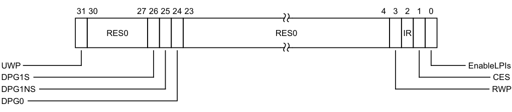
Image text
31 30 27 26 25 24 23 4 3 2 1 0
RES0 RES0 IR
UWP EnableLPIs
DPG1S CES
DPG1NS RWP
DPG0
0b0 The effects of all upstream writes have been communicated to the Distributor, including any Generate SGI packets. For more information, see _Generate SGI (ICC)_A-883.
0b1 Not all the effects of upstream writes, including any Generate SGI packets, have been communicated to the Distributor. For more information, see _Generate SGI (ICC)_A-883.
Bits [30:27]
Reserved, RES0.
DPG1S, bit [26]
Disable Processor selection for Group 1 Secure interrupts. When GICR_TYPER.DPGS == 1:
0b0 A Group 1 Secure SPI configured to use the 1 of N distribution model can select this PE, if the PE is not asleep and if Secure Group 1 interrupts are enabled.
0b1 A Group 1 Secure SPI configured to use the 1 of N distribution model cannot select this PE.
When GICR_TYPER.DPGS == 0 this bit is RAZ/WI.
When GICD_CTLR.DS==1, this field is RAZ/WI. In GIC implementations that support two Security states, this field is only accessible by Secure accesses, and is RAZ/WI to Non-secure accesses.
It is IMPLEMENTATION DEFINED whether these bits affect the selection of PEs for interrupts using the 1 of N distribution model when GICD_CTLR.ARE_S==0.
On a Warm reset, this field resets to 0.
DPG1NS, bit [25]
Disable Processor selection for Group 1 Non-secure interrupts. When GICR_TYPER.DPGS == 1:
0b0 A Group 1 Non-secure SPI configured to use the 1 of N distribution model can select this PE, if the PE is not asleep and if Non-secure Group 1 interrupts are enabled.
0b1 A Group 1 Non-secure SPI configured to use the 1 of N distribution model cannot select this PE.
When GICR_TYPER.DPGS == 0 this bit is RAZ/WI.
It is IMPLEMENTATION DEFINED whether these bits affect the selection of PEs for interrupts using the 1 of N distribution model when GICD_CTLR.ARE_NS==0.
On a Warm reset, this field resets to 0.
DPG0, bit [24]
Disable Processor selection for Group 0 interrupts. When GICR_TYPER.DPGS == 1:
0b0 A Group 0 SPI configured to use the 1 of N distribution model can select this PE, if the PE is not asleep and if Group 0 interrupts are enabled.
0b1 A Group 0 SPI configured to use the 1 of N distribution model cannot select this PE. When GICR_TYPER.DPGS == 0 this bit is RAZ/WI.
When GICD_CTLR.DS == 1, this field is always accessible. In GIC implementations that support two Security states, this field is RAZ/WI to Non-secure accesses.
It is IMPLEMENTATION DEFINED whether these bits affect the selection of PEs for interrupts using the 1 of N distribution model when GICD_CTLR.ARE_S == 0.
On a Warm reset, this field resets to 0.
Bits [23:4]
Reserved, RES0.
RWP, bit [3]
Register Write Pending. This bit indicates whether a register write for the current Security state is in progress or not.
0b0 The effect of all previous writes to the following registers are visible to all agents in the system:
-
GICR_ICENABLER0
-
• GICR_CTLR.DPG1S • GICR_CTLR.DPG1NS • GICR_CTLR.DPG0 • GICR_CTLR, which clears EnableLPIs from 1 to 0. • In FEAT_GICv4p1, GICR_VPROPBASER, which clears Valid from 1 to 0.
-
0b1 The effect of all previous writes to the following registers are not guaranteed by the architecture to be visible to all agents in the system while the changes are still being propagated:
-
GICR_ICENABLER0
-
GICR_CTLR.DPG1S
-
• GICR_CTLR.DPG1NS • GICR_CTLR.DPG0 • GICR_CTLR, which clears EnableLPIs from 1 to 0.
-
In FEAT_GICv4p1, GICR_VPROPBASER, which clears Valid from 1 to 0.
-
IR, bit [2]
LPI invaldiate registers supported. This bit is read-only.
0b0 This bit does not indicate whether the GICR_INVLPIR, GICR_INVALLR and GICR_SYNCR are implemented or not.
0b1 GICR_INVLPIR, GICR_INVALLR and GICR_SYNCR are implemented. If GICR_TYPER.DirectLPI is 1 or GICR_TYPER.RVPEI is 1, GICR_INVLPIR, GICR_INVALLR, and GICR_SYNCR are always implemented.
Arm recommends that implementations report GICR_CTLR.IR as 1 in these cases.
CES, bit [1]
Clear Enable Supported.
This bit is read-only.
0b0 The IRI does not indicate whether GICR_CTLR.EnableLPIs is RES1 once set.
- 0b1 GICR_CTLR.EnableLPIs is not RES1 once set.
Implementing GICR_CTLR.EnableLPIs as programmable and not reporting GICR_CLTR.CES == 1 is deprecated.
Implementing GICR_CTLR.EnableLPIs as RES1 once set is deprecated.
When GICR_CLTR.CES == 0, software cannot assume that GICR_CTLR.EnableLPIs is programmable without observing the bit being cleared.
EnableLPIs, bit [0]
In implementations where affinity routing is enabled for the Security state:
0b0 LPI support is disabled. Any doorbell interrupt generated as a result of a write to a virtual LPI register must be discarded, and any ITS translation requests or commands involving LPIs in this Redistributor are ignored.
0b1 LPI support is enabled.
Note If GICR_TYPER.PLPIS == 0, this field is RES0. If GICD_CTLR.ARE_NS is written from 1 to 0 when this bit is 1, behavior is an IMPLEMENTATION DEFINED choice between clearing GICR_CTLR.EnableLPIs to 0 or maintaining its current value.
When affinity routing is not enabled for the Non-secure state, this bit is RES0.
When written from 0 to 1, the Redistributor loads the LPI Pending table from memory to check for any pending interrupts.
After it has been written to 1, it is IMPLEMENTATION DEFINED whether the bit becomes RES1 or can be cleared by to 0.
Where the bit remains programmable:
-
Software must observe GICR_CTLR.RWP==0 after clearing GICR_CTLR.EnableLPIs from 1 to 0 before writing GICR_PENDBASER or GICR_PROPBASER, otherwise behavior is UNPREDICTABLE.
-
Software must observe GICR_CTLR.RWP==0 after clearing GICR_CTLR.EnableLPIs from 1 to 0 before setting GICR_CTLR.EnableLPIs to 1, otherwise behavior is UNPREDICTABLE.
Note If one or more ITS is implemented, Arm strongly recommends that all LPIs are mapped to another Redistributor before GICR_CTLR.EnableLPIs is cleared to 0.
On a Warm reset, this field resets to 0. The participation of a PE in the 1 of N distribution model for a given interrupt group is governed by the concatenation of GICR_WAKER.ProcessorSleep, the appropriate GICR_CTLR.DPG{1, 0} bit, and the PE interrupt group enable. The behavior options are:
| PS | DPG{1S, | 1NS, | 0} | Enable | PE Behavior |
|---|---|---|---|---|---|
| 0b0 | 0b0 | 0b0 | The PE cannot be selected. | ||
| 0b0 | 0b0 | 0b1 | The PE can be selected. | ||
| 0b0 | 0b1 | * | The PE cannot be selected. | ||
| 0b1 | * | * | The PE cannot be selected whenGICD_CTLR.E1NWF == 0. When GICD_CTLR.E1NWF == 1, the mechanism by which PEs are selected isIMPLEMENTATION DEFINED. |
If an SPI using the 1 of N distribution model has been forwarded to the PE, and a write to GICR_CTLR occurs that changes the DPG bit for the interrupt group of the SPI, the IRI must attempt to select a different target PE for the SPI. This might have no effect on the forwarded SPI if it has already been activated.
Accessing the GICR_CTLR:
GICR_CTLR can be accessed through its memory-mapped interface:
| Component | Frame | Offset | Instance |
|---|---|---|---|
| GIC Redistributor | RD_base | 0x0000 | GICR_CTLR |
This interface is accessible as follows:
-
When GICD_CTLR.DS == 0 accesses to this register are RW.
-
When an access is Secure accesses to this register are RW.
-
When an access is Non-secure accesses to this register are RW.
12.11.3 GICR_ICACTIVER0, Interrupt Clear-Active Register 0
The GICR_ICACTIVER0 characteristics are:
Purpose
Deactivates the corresponding SGI or PPI. These registers are used when saving and restoring GIC state.
Configurations
A copy of this register is provided for each Redistributor.
Attributes
GICR_ICACTIVER0 is a 32-bit register.
Field descriptions
The GICR_ICACTIVER0 bit assignments are:
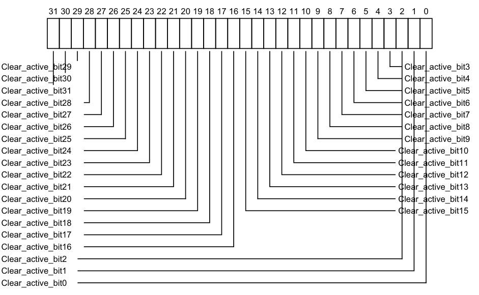
Image text
31 30 29 28 27 26 25 24 23 22 21 20 19 18 17 16 15 14 13 12 11 10 9 8 7 6 5 4 3 2 1 0
Clear_active_bit29 Clear_active_bit3
Clear_active_bit30 Clear_active_bit4
Clear_active_bit31 Clear_active_bit5
Clear_active_bit28 Clear_active_bit6
Clear_active_bit27 Clear_active_bit7
Clear_active_bit26 Clear_active_bit8
Clear_active_bit25 Clear_active_bit9
Clear_active_bit24 Clear_active_bit10
Clear_active_bit23 Clear_active_bit11
Clear_active_bit22 Clear_active_bit12
Clear_active_bit21 Clear_active_bit13
Clear_active_bit20 Clear_active_bit14
Clear_active_bit19 Clear_active_bit15
Clear_active_bit18
Clear_active_bit17
Clear_active_bit16
Clear_active_bit2
Clear_active_bit1
Clear_active_bit0
0b0 If read, indicates that the corresponding interrupt is not active, and is not active and pending.
If written, has no effect.
0b1 If read, indicates that the corresponding interrupt is active, or is active and pending. If written, deactivates the corresponding interrupt, if the interrupt is active. If the interrupt is already deactivated, the write has no effect.
On a Warm reset, this field resets to an architecturally UNKNOWN value.
Accessing the GICR_ICACTIVER0:
When affinity routing is not enabled for the Security state of an interrupt in GICR_ICACTIVER0, the corresponding bit is RAZ/WI and equivalent functionality is provided by GICD_ICACTIVER
This register only applies to SGIs (bits [15:0]) and PPIs (bits [31:16]). For SPIs, this functionality is provided by GICD_ICACTIVER
When GICD_CTLR.DS == 0, bits corresponding to Secure SGIs and PPIs are RAZ/WI to Non-secure accesses.
GICR_ICACTIVER0 can be accessed through its memory-mapped interface:
| Component | Frame | Offset | Instance |
|---|---|---|---|
| GIC Redistributor | SGI_base | 0x0380 | GICR_ICACTIVER0 |
This interface is accessible as follows:
-
When GICD_CTLR.DS == 0 accesses to this register are RW.
-
When an access is Secure accesses to this register are RW.
-
When an access is Non-secure accesses to this register are RW.
12.11.4 GICR_ICACTIVERE, Interrupt Clear-Active Registers, n = 1 - 2
The GICR_ICACTIVER
Purpose
Removes the active state from the corresponding PPI.
Configurations
This register is present only when FEAT_GICv3p1 is implemented. Otherwise, direct accesses to GICR_ICACTIVER
A copy of this register is provided for each Redistributor.
Attributes
GICR_ICACTIVER
Field descriptions
The GICR_ICACTIVER

Image text
31 30 29 28 27 26 25 24 23 22 21 20 19 18 17 16 15 14 13 12 11 10 9 8 7 6 5 4 3 2 1 0
Clear_active_bit29 Clear_active_bit3
Clear_active_bit30 Clear_active_bit4
Clear_active_bit31 Clear_active_bit5
Clear_active_bit28 Clear_active_bit6
Clear_active_bit27 Clear_active_bit7
Clear_active_bit26 Clear_active_bit8
Clear_active_bit25 Clear_active_bit9
Clear_active_bit24 Clear_active_bit10
Clear_active_bit23 Clear_active_bit11
Clear_active_bit22 Clear_active_bit12
Clear_active_bit21 Clear_active_bit13
Clear_active_bit20 Clear_active_bit14
Clear_active_bit19 Clear_active_bit15
Clear_active_bit18
Clear_active_bit17
Clear_active_bit16
Clear_active_bit2
Clear_active_bit1
Clear_active_bit0
0b0 If read, indicates that the corresponding interrupt is not active, and is not active and pending.
If written, has no effect.
0b1 If read, indicates that the corresponding interrupt is active, or is active and pending. If written, deactivates the corresponding interrupt, if the interrupt is active. If the interrupt is already deactivated, the write has no effect.
On a Warm reset, this field resets to an architecturally UNKNOWN value. For INTID m, when DIV and MOD are the integer division and modulo operations:
-
The corresponding GICR_ICACTIVER
E number, n, is given by n = (m-1024) DIV 32. -
The offset of the required GICR_ICACTIVER
E is (0x200 + (4*n)). -
The bit number of the required group modifier bit in this register is (m-1024) MOD 32.
Accessing the GICR_ICACTIVERE:
When affinity routing is not enabled for the Security state of an interrupt in GICR_ICACTIVER
When GICD_CTLR.DS==0, bits corresponding to Secure PPIs are RAZ/WI to Non-secure accesses.
Bits corresponding to unimplemented interrupts are RAZ/WI.
GICR_ICACTIVER
Component Frame Offset Instance
GIC Redistributor SGI_base 0x0380 + (4 * n) GICR_ICACTIVER
This interface is accessible as follows:
-
When GICD_CTLR.DS == 0 accesses to this register are RW.
-
When an access is Secure accesses to this register are RW.
-
When an access is Non-secure accesses to this register are RW.
12.11.5 GICR_ICENABLER0, Interrupt Clear-Enable Register 0
The GICR_ICENABLER0 characteristics are:
Purpose
Disables forwarding of the corresponding SGI or PPI to the CPU interfaces.
Configurations
A copy of this register is provided for each Redistributor.
Attributes
GICR_ICENABLER0 is a 32-bit register.
Field descriptions
The GICR_ICENABLER0 bit assignments are:

Image text
31 30 29 28 27 26 25 24 23 22 21 20 19 18 17 16 15 14 13 12 11 10 9 8 7 6 5 4 3 2 1 0
Clear_enable_bit29 Clear_enable_bit3
Clear_enable_bit30 Clear_enable_bit4
Clear_enable_bit31 Clear_enable_bit5
Clear_enable_bit28 Clear_enable_bit6
Clear_enable_bit27 Clear_enable_bit7
Clear_enable_bit26 Clear_enable_bit8
Clear_enable_bit25 Clear_enable_bit9
Clear_enable_bit24 Clear_enable_bit10
Clear_enable_bit23 Clear_enable_bit11
Clear_enable_bit22 Clear_enable_bit12
Clear_enable_bit21 Clear_enable_bit13
Clear_enable_bit20 Clear_enable_bit14
Clear_enable_bit19 Clear_enable_bit15
Clear_enable_bit18
Clear_enable_bit17
Clear_enable_bit16
Clear_enable_bit2
Clear_enable_bit1
Clear_enable_bit0
0b0 If read, indicates that forwarding of the corresponding interrupt is disabled. If written, has no effect.
0b1 If read, indicates that forwarding of the corresponding interrupt is enabled. If written, disables forwarding of the corresponding interrupt. After a write of 1 to this bit, a subsequent read of this bit returns 0.
On a Warm reset, this field resets to an architecturally UNKNOWN value.
Accessing the GICR_ICENABLER0:
When affinity routing is not enabled for the Security state of an interrupt in GICR_ICENABLER0, the corresponding bit is RAZ/WI and equivalent functionality is provided by GICD_ICENABLER
This register only applies to SGIs (bits [15:0]) and PPIs (bits [31:16]). For SPIs, this functionality is provided by GICD_ICENABLER
When GICD_CTLR.DS == 0, bits corresponding to Secure SGIs and PPIs are RAZ/WI to Non-secure accesses.
GICR_ICENABLER0 can be accessed through its memory-mapped interface:
| Component | Frame | Offset | Instance |
|---|---|---|---|
| GIC Redistributor | SGI_base | 0x0180 | GICR_ICENABLER0 |
This interface is accessible as follows:
-
When GICD_CTLR.DS == 0 accesses to this register are RW.
-
When an access is Secure accesses to this register are RW.
-
When an access is Non-secure accesses to this register are RW.
12.11.6 GICR_ICENABLERE, Interrupt Clear-Enable Registers, n = 1 - 2
The GICR_ICENABLER
Purpose
Disables forwarding of the corresponding PPI to the CPU interfaces.
Configurations
This register is present only when FEAT_GICv3p1 is implemented. Otherwise, direct accesses to GICR_ICENABLER
A copy of this register is provided for each Redistributor.
Attributes
GICR_ICENABLER
Field descriptions
The GICR_ICENABLER
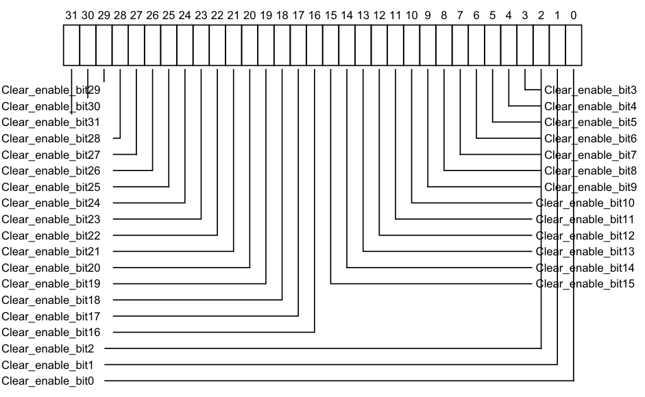
Image text
31 30 29 28 27 26 25 24 23 22 21 20 19 18 17 16 15 14 13 12 11 10 9 8 7 6 5 4 3 2 1 0
Clear_enable_bit29 Clear_enable_bit3
Clear_enable_bit30 Clear_enable_bit4
Clear_enable_bit31 Clear_enable_bit5
Clear_enable_bit28 Clear_enable_bit6
Clear_enable_bit27 Clear_enable_bit7
Clear_enable_bit26 Clear_enable_bit8
Clear_enable_bit25 Clear_enable_bit9
Clear_enable_bit24 Clear_enable_bit10
Clear_enable_bit23 Clear_enable_bit11
Clear_enable_bit22 Clear_enable_bit12
Clear_enable_bit21 Clear_enable_bit13
Clear_enable_bit20 Clear_enable_bit14
Clear_enable_bit19 Clear_enable_bit15
Clear_enable_bit18
Clear_enable_bit17
Clear_enable_bit16
Clear_enable_bit2
Clear_enable_bit1
Clear_enable_bit0
0b0 If read, indicates that forwarding of the corresponding interrupt is disabled. If written, has no effect.
0b1 If read, indicates that forwarding of the corresponding interrupt is enabled. If written, disables forwarding of the corresponding interrupt. After a write of 1 to this bit, a subsequent read of this bit returns 0.
On a Warm reset, this field resets to 0. For INTID m, when DIV and MOD are the integer division and modulo operations:
-
The corresponding GICR_ICENABLER
E number, n, is given by n = (m-1024) DIV 32. -
The offset of the required GICR_ICENABLER
E is (0x180 + (4*n)). -
The bit number of the required group modifier bit in this register is (m-1024) MOD 32.
Accessing the GICR_ICENABLERE:
When affinity routing is not enabled for the Security state of an interrupt in GICR_ICENABLER
When GICD_CTLR.DS==0, bits corresponding to Secure PPIs are RAZ/WI to Non-secure accesses.
Bits corresponding to unimplemented interrupts are RAZ/WI.
GICR_ICENABLER
Component Frame Offset Instance
GIC Redistributor SGI_base 0x0180 + (4 * n) GICR_ICENABLER
This interface is accessible as follows:
-
When GICD_CTLR.DS == 0 accesses to this register are RW.
-
When an access is Secure accesses to this register are RW.
-
When an access is Non-secure accesses to this register are RW.
12.11.7 GICR_ICFGR0, Interrupt Configuration Register 0
The GICR_ICFGR0 characteristics are:
Purpose
Determines whether the corresponding SGI is edge-triggered or level-sensitive.
Configurations
A copy of this register is provided for each Redistributor.
Attributes
GICR_ICFGR0 is a 32-bit register.
Field descriptions
The GICR_ICFGR0 bit assignments are:

Image text
31 30 29 28 27 26 25 24 23 22 21 20 19 18 17 16 15 14 13 12 11 10 9 8 7 6 5 4 3 2 1 0
Int_config15 Int_config1
Int_config14 Int_config2
Int_config13 Int_config3
Int_config12 Int_config4
Int_config11 Int_config5
Int_config10 Int_config6
Int_config9 Int_config7
Int_config8
Int_config0
Int_config[0] (bit [2x]) is RES0.
Possible values of Int_config[1] (bit [2x+1]) are:
0b00 Corresponding interrupt is level-sensitive. 0b01 Corresponding interrupt is edge-triggered.
For SGIs, Int_config[1] is RAO/WI.
A read of this bit always returns the correct value to indicate the interrupt triggering method. On a Warm reset, this field resets to an architecturally UNKNOWN value.
Accessing the GICR_ICFGR0:
This register is used when affinity routing is enabled.
When affinity routing is disabled for the Security state of an interrupt, the field for that interrupt is RES0 and an implementation is permitted to make the field RAZ/WI in this case. Equivalent functionality is provided by GICD_ICFGR
When GICD_CTLR.DS==0, a register bit that corresponds to a Group 0 or Secure Group 1 interrupt is RAZ/WI to Non-secure accesses. GICR_ICFGR0 can be accessed through its memory-mapped interface:
| Component | Frame | Offset | Instance |
|---|---|---|---|
| GIC Redistributor | SGI_base | 0x0C00 | GICR_ICFGR0 |
This interface is accessible as follows:
-
When GICD_CTLR.DS == 0 accesses to this register are RW.
-
When an access is Secure accesses to this register are RW.
-
When an access is Non-secure accesses to this register are RW.
12.11.8 GICR_ICFGR1, Interrupt Configuration Register 1
The GICR_ICFGR1 characteristics are:
Purpose
Determines whether the corresponding PPI is edge-triggered or level-sensitive.
Configurations
A copy of this register is provided for each Redistributor.
For each supported PPI, it is IMPLEMENTATION DEFINED whether software can program the corresponding Int_config field.
Changing Int_config when the interrupt is individually enabled is UNPREDICTABLE.
Changing the interrupt configuration between level-sensitive and edge-triggered (in either direction) at a time when there is a pending interrupt will leave the interrupt in an UNKNOWN pending state.
Attributes
GICR_ICFGR1 is a 32-bit register.
Field descriptions
The GICR_ICFGR1 bit assignments are:

Image text
31 30 29 28 27 26 25 24 23 22 21 20 19 18 17 16 15 14 13 12 11 10 9 8 7 6 5 4 3 2 1 0
Int_config15 Int_config1
Int_config14 Int_config2
Int_config13 Int_config3
Int_config12 Int_config4
Int_config11 Int_config5
Int_config10 Int_config6
Int_config9 Int_config7
Int_config8
Int_config0
Int_config[0] (bit [2x]) is RES0.
Possible values of Int_config[1] (bit [2x+1]) are:
0b00 Corresponding interrupt is level-sensitive.
0b01 Corresponding interrupt is edge-triggered.
A read of this bit always returns the correct value to indicate the interrupt triggering method.
For PPIs, Int_config[1] is programmable unless the implementation supports two Security states and the bit corresponds to a Group 0 or Secure Group 1 interrupt, in which case the bit is RAZ/WI to Non-secure accesses.
On a Warm reset, this field resets to an architecturally UNKNOWN value.
Accessing the GICR_ICFGR1:
This register is used when affinity routing is enabled.
When affinity routing is disabled for the Security state of an interrupt, the field for that interrupt is RES0 and an implementation is permitted to make the field RAZ/WI in this case. Equivalent functionality is provided by GICD_ICFGR
GICR_ICFGR1 can be accessed through its memory-mapped interface:
| Component | Frame | Offset | Instance |
|---|---|---|---|
| GIC Redistributor | SGI_base | 0x0C04 | GICR_ICFGR1 |
This interface is accessible as follows:
-
When GICD_CTLR.DS == 0 accesses to this register are RW.
-
When an access is Secure accesses to this register are RW.
-
When an access is Non-secure accesses to this register are RW.
12.11.9 GICR_ICFGRE, Interrupt configuration registers, n = 2 - 5
The GICR_ICFGR
Purpose
Determines whether the corresponding PPI in the extended PPI range is edge-triggered or level-sensitive.
Configurations
This register is present only when FEAT_GICv3p1 is implemented. Otherwise, direct accesses to GICR_ICFGR
A copy of this register is provided for each Redistributor.
Attributes
GICR_ICFGR
Field descriptions
The GICR_ICFGR
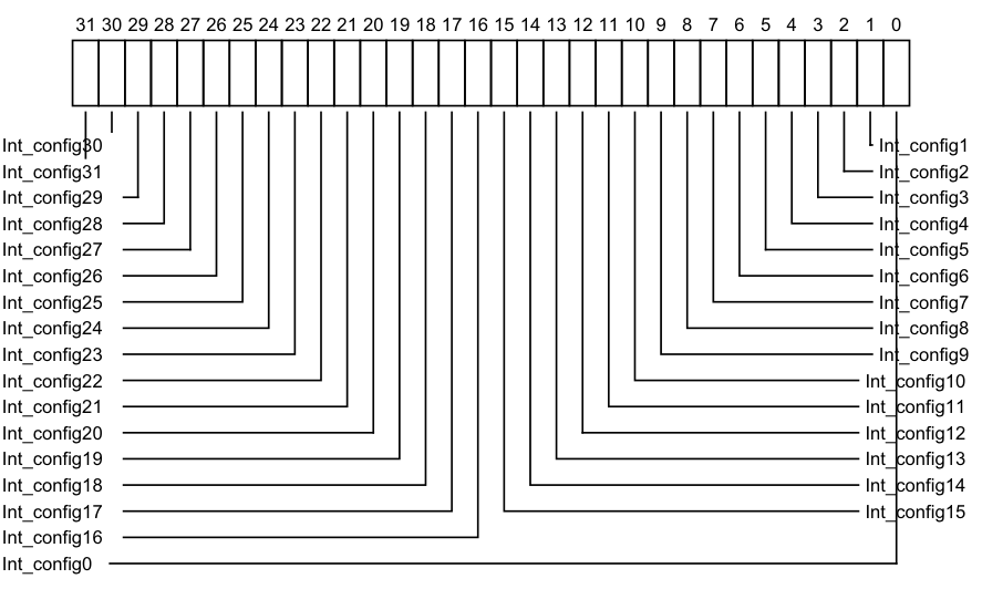
Image text
31 30 29 28 27 26 25 24 23 22 21 20 19 18 17 16 15 14 13 12 11 10 9 8 7 6 5 4 3 2 1 0
Int_config30 Int_config1
Int_config31 Int_config2
Int_config29 Int_config3
Int_config28 Int_config4
Int_config27 Int_config5
Int_config26 Int_config6
Int_config25 Int_config7
Int_config24 Int_config8
Int_config23 Int_config9
Int_config22 Int_config10
Int_config21 Int_config11
Int_config20 Int_config12
Int_config19 Int_config13
Int_config18 Int_config14
Int_config17 Int_config15
Int_config16
Int_config0
Int_config[0] (bit [2x]) is RES0.
Possible values of Int_config[1] (bit [2x+1]) are:
0b0 The corresponding interrupt is level-sensitive.
0b1 The corresponding interrupt is edge-triggered.
On a Warm reset, this field resets to an architecturally UNKNOWN value.
For each supported extended PPI, it is IMPLEMENTATION DEFINED whether software can program the corresponding Int_config field.
Accessing the GICR_ICFGRE:
When affinity routing is not enabled for the Security state of an interrupt in GICR_ICFGR
When GICD_CTLR.DS==0, a register bit that corresponds to a Group 0 or Secure Group 1 interrupt is RAZ/WI to Non-secure accesses.
Bits corresponding to unimplemented interrupts are RAZ/WI.
GICR_ICFGR
Component Frame Offset Instance GIC Redistributor SGI_base 0x0C00 + (4 * n) GICR_ICFGR
This interface is accessible as follows:
-
When GICD_CTLR.DS == 0 accesses to this register are RW.
-
When an access is Secure accesses to this register are RW.
-
When an access is Non-secure accesses to this register are RW.
12.11.10 GICR_ICPENDR0, Interrupt Clear-Pending Register 0
The GICR_ICPENDR0 characteristics are:
Purpose
Removes the pending state from the corresponding SGI or PPI.
Configurations
A copy of this register is provided for each Redistributor.
Attributes
GICR_ICPENDR0 is a 32-bit register.
Field descriptions
The GICR_ICPENDR0 bit assignments are:
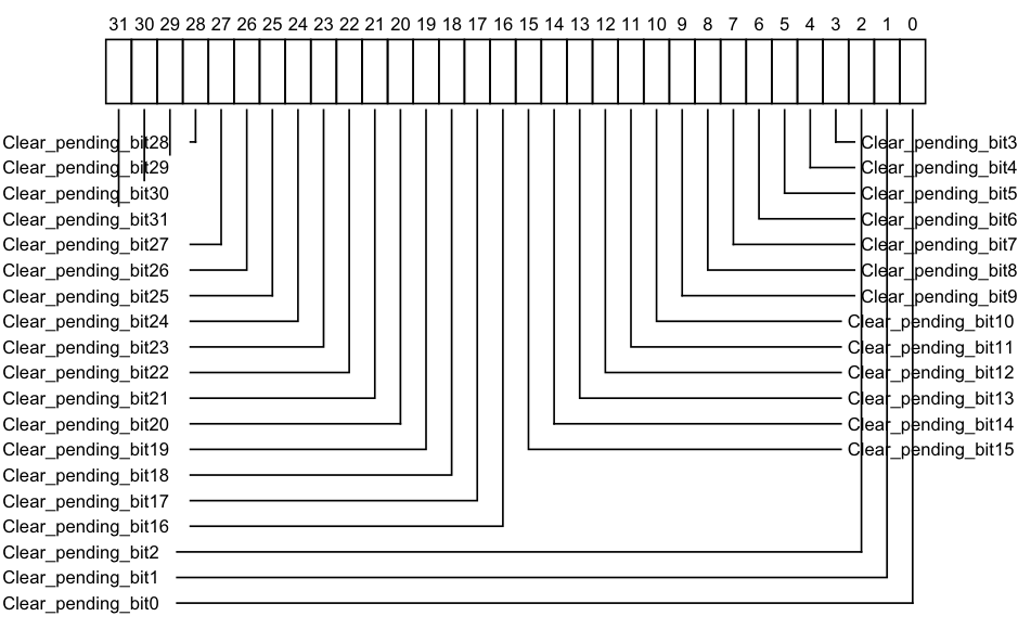
Image text
31 30 29 28 27 26 25 24 23 22 21 20 19 18 17 16 15 14 13 12 11 10 9 8 7 6 5 4 3 2 1 0
Clear_pending_bit28 Clear_pending_bit3
Clear_pending_bit29 Clear_pending_bit4
Clear_pending_bit30 Clear_pending_bit5
Clear_pending_bit31 Clear_pending_bit6
Clear_pending_bit27 Clear_pending_bit7
Clear_pending_bit26 Clear_pending_bit8
Clear_pending_bit25 Clear_pending_bit9
Clear_pending_bit24 Clear_pending_bit10
Clear_pending_bit23 Clear_pending_bit11
Clear_pending_bit22 Clear_pending_bit12
Clear_pending_bit21 Clear_pending_bit13
Clear_pending_bit20 Clear_pending_bit14
Clear_pending_bit19 Clear_pending_bit15
Clear_pending_bit18
Clear_pending_bit17
Clear_pending_bit16
Clear_pending_bit2
Clear_pending_bit1
Clear_pending_bit0
-
0b0 If read, indicates that the corresponding interrupt is not pending. If written, has no effect.
-
0b1
-
If read, indicates that the corresponding interrupt is pending, or active and pending. If written, changes the state of the corresponding interrupt from pending to inactive, or from active and pending to active. This has no effect in the following cases:
-
If the interrupt is not pending and is not active and pending.
-
If the interrupt is a level-sensitive interrupt that is pending or active and pending for a reason other than a write to GICD_ISPENDR
. In this case, if the interrupt signal continues to be asserted, the interrupt remains pending or active and pending.
On a Warm reset, this field resets to an architecturally UNKNOWN value.
Accessing the GICR_ICPENDR0:
When affinity routing is not enabled for the Security state of an interrupt in GICR_ICPENDR0, the corresponding bit is RAZ/WI and equivalent functionality is provided by GICD_ICPENDR
This register only applies to SGIs (bits [15:0]) and PPIs (bits [31:16]). For SPIs, this functionality is provided by GICD_ICENABLER
When GICD_CTLR.DS == 0, bits corresponding to Secure SGIs and PPIs are RAZ/WI to Non-secure accesses.
GICR_ICPENDR0 can be accessed through its memory-mapped interface:
| Component | Frame | Offset | Instance |
|---|---|---|---|
| GIC Redistributor | SGI_base | 0x0280 | GICR_ICPENDR0 |
This interface is accessible as follows:
-
When GICD_CTLR.DS == 0 accesses to this register are RW.
-
When an access is Secure accesses to this register are RW.
-
When an access is Non-secure accesses to this register are RW.
12.11.11 GICR_ICPENDRE, Interrupt Clear-Pending Registers, n = 1 - 2
The GICR_ICPENDR
Purpose
Removes the pending state from the corresponding PPI.
Configurations
This register is present only when FEAT_GICv3p1 is implemented. Otherwise, direct accesses to GICR_ICPENDR
A copy of this register is provided for each Redistributor.
Attributes
GICR_ICPENDR
Field descriptions
The GICR_ICPENDR

Image text
31 30 29 28 27 26 25 24 23 22 21 20 19 18 17 16 15 14 13 12 11 10 9 8 7 6 5 4 3 2 1 0
Clear_pending_bit28 Clear_pending_bit3
Clear_pending_bit29 Clear_pending_bit4
Clear_pending_bit30 Clear_pending_bit5
Clear_pending_bit31 Clear_pending_bit6
Clear_pending_bit27 Clear_pending_bit7
Clear_pending_bit26 Clear_pending_bit8
Clear_pending_bit25 Clear_pending_bit9
Clear_pending_bit24 Clear_pending_bit10
Clear_pending_bit23 Clear_pending_bit11
Clear_pending_bit22 Clear_pending_bit12
Clear_pending_bit21 Clear_pending_bit13
Clear_pending_bit20 Clear_pending_bit14
Clear_pending_bit19 Clear_pending_bit15
Clear_pending_bit18
Clear_pending_bit17
Clear_pending_bit16
Clear_pending_bit2
Clear_pending_bit1
Clear_pending_bit0
-
0b0 If read, indicates that the corresponding interrupt is not pending on this PE. If written, has no effect.
-
0b1 If read, indicates that the corresponding interrupt is pending, or active and pending on this PE.
If written, changes the state of the corresponding interrupt from pending to inactive, or from active and pending to active.
This has no effect in the following cases:
- If the interrupt is not pending and is not active and pending.
- If the interrupt is a level-sensitive interrupt that is pending or active and pending for a reason other than a write to GICR_ISPENDR
E. In this case, if the interrupt signal continues to be asserted, the interrupt remains pending or active and pending.
On a Warm reset, this field resets to an architecturally UNKNOWN value.
For INTID m, when DIV and MOD are the integer division and modulo operations:
-
The corresponding GICR_ICPENDR
E number, n, is given by n = (m-1024) DIV 32. -
The offset of the required GICR_ICPENDR
E is (0x200 + (4*n)). -
The bit number of the required group modifier bit in this register is (m-1024) MOD 32.
Accessing the GICR_ICPENDRE:
When affinity routing is not enabled for the Security state of an interrupt in GICR_ICPENDR
When GICD_CTLR.DS==0, bits corresponding to Secure PPIs are RAZ/WI to Non-secure accesses.
Bits corresponding to unimplemented interrupts are RAZ/WI.
GICR_ICPENDR
Component Frame Offset Instance GIC Redistributor SGI_base 0x0280 + (4 * n) GICR_ICPENDR
This interface is accessible as follows:
-
When GICD_CTLR.DS == 0 accesses to this register are RW.
-
When an access is Secure accesses to this register are RW.
-
When an access is Non-secure accesses to this register are RW.
12.11.12 GICR_IGROUPR0, Interrupt Group Register 0
The GICR_IGROUPR0 characteristics are:
Purpose
Controls whether the corresponding SGI or PPI is in Group 0 or Group 1.
Configurations
This register is available in all GIC configurations. If the GIC implementation supports two Security states, this register is Secure.
A copy of this register is provided for each Redistributor.
Attributes
GICR_IGROUPR0 is a 32-bit register.
Field descriptions
The GICR_IGROUPR0 bit assignments are:
31 30 29 28 27 26 25 24 23 22 21 20 19 18 17 16 15 14 13 12 11 10 9 8 7 6 5 4 3 2 1 0 Redistributor_group_status_bit27 Redistributor_group_status_bit5 Redistributor_group_status_bit28 Redistributor_group_status_bit6 Redistributor_group_status_bit29 Redistributor_group_status_bit7 Redistributor_group_status_bit30 Redistributor_group_status_bit8 Redistributor_group_status_bit31 Redistributor_group_status_bit9 Redistributor_group_status_bit26 Redistributor_group_status_bit10 Redistributor_group_status_bit25 Redistributor_group_status_bit11 Redistributor_group_status_bit24 Redistributor_group_status_bit12 Redistributor_group_status_bit23 Redistributor_group_status_bit13 Redistributor_group_status_bit22 Redistributor_group_status_bit14 Redistributor_group_status_bit21 Redistributor_group_status_bit15 Redistributor_group_status_bit20 Redistributor_group_status_bit19 Redistributor_group_status_bit18 Redistributor_group_status_bit17 Redistributor_group_status_bit16 Redistributor_group_status_bit4 Redistributor_group_status_bit3 Redistributor_group_status_bit2 Redistributor_group_status_bit1 Redistributor_group_status_bit0
Redistributor_group_status_bit, bit [x], for x = 31 to 0
Group status bit. In this register:
-
Bits [31:16] are group status bits for PPIs.
-
Bits [15:0] are group status bits for SGIs.
-
0b0 When GICD_CTLR.DS==1, the corresponding interrupt is Group 0. When GICD_CTLR.DS==0, the corresponding interrupt is Secure.
-
0b1 When GICD_CTLR.DS==1, the corresponding interrupt is Group 1. When GICD_CTLR.DS==0, the corresponding interrupt is Non-secure Group 1. When GICD_CTLR.DS == 0, the bit that corresponds to the interrupt is concatenated with the equivalent bit in GICR_IGRPMODR0 to form a 2-bit field that defines an interrupt group. The encoding of this field is at GICR_IGRPMODR0.
On a Warm reset, this field resets to an architecturally UNKNOWN value.
The considerations for the reset value of this register are the same as those for GICD_IGROUPR
Accessing the GICR_IGROUPR0:
When affinity routing is not enabled for the Security state of an interrupt in GICR_IGROUPR0, the corresponding bit is RES0 and equivalent functionality is provided by GICD_IGROUPR
When GICD_CTLR.DS == 0, the register is RAZ/WI to Non-secure accesses.
Bits corresponding to unimplemented interrupts are RAZ/WI.
Note Implementations must ensure that an interrupt that is pending at the time of the write uses either the old value or the new value and must ensure that the interrupt is neither lost nor handled more than one time. The effect of the change must be visible in finite time.
GICR_IGROUPR0 can be accessed through its memory-mapped interface:
Component Frame Offset Instance GIC Redistributor SGI_base 0x0080 GICR_IGROUPR0
This interface is accessible as follows:
-
When GICD_CTLR.DS == 0 accesses to this register are RW.
-
When an access is Secure accesses to this register are RW.
-
When an access is Non-secure accesses to this register are RW.
12.11.13 GICR_IGROUPRE, Interrupt Group Registers, n = 1 - 2
The GICR_IGROUPR
Purpose
Controls whether the corresponding PPI is in Group 0 or Group 1.
Configurations
This register is present only when FEAT_GICv3p1 is implemented. Otherwise, direct accesses to GICR_IGROUPR
When GICD_CTLR.DS==0, this register is Secure.
A copy of this register is provided for each Redistributor.
Attributes
GICR_IGROUPR
Field descriptions
The GICR_IGROUPR

Image text
31 30 29 28 27 26 25 24 23 22 21 20 19 18 17 16 15 14 13 12 11 10 9 8 7 6 5 4 3 2 1 0
Group_status_bit29 Group_status_bit3
Group_status_bit30 Group_status_bit4
Group_status_bit31 Group_status_bit5
Group_status_bit28 Group_status_bit6
Group_status_bit27 Group_status_bit7
Group_status_bit26 Group_status_bit8
Group_status_bit25 Group_status_bit9
Group_status_bit24 Group_status_bit10
Group_status_bit23 Group_status_bit11
Group_status_bit22 Group_status_bit12
Group_status_bit21 Group_status_bit13
Group_status_bit20 Group_status_bit14
Group_status_bit19 Group_status_bit15
Group_status_bit18
Group_status_bit17
Group_status_bit16
Group_status_bit2
Group_status_bit1
Group_status_bit0
0b0 When GICD_CTLR.DS==1, the corresponding interrupt is Group 0. When GICD_CTLR.DS==0, the corresponding interrupt is Secure.
0b1 When GICD_CTLR.DS==1, the corresponding interrupt is Group 1. When GICD_CTLR.DS==0, the corresponding interrupt is Non-secure Group 1.
On a Warm reset, this field resets to an architecturally UNKNOWN value.
If affinity routing is enabled for the Security state of an interrupt, the bit that corresponds to the interrupt is concatenated with the equivalent bit in GICR_IGRPMODR
If affinity routing is disabled for the Security state of an interrupt, the bit is RES0.
For INTID m, when DIV and MOD are the integer division and modulo operations:
-
The corresponding GICR_IGROUPR
E number, n, is given by n = (m-1024) DIV 32. -
The offset of the required GICR_IGROUPR
E is (0x080 + (4*n)). -
The bit number of the required group modifier bit in this register is (m-1024) MOD 32.
Accessing the GICR_IGROUPRE:
When affinity routing is not enabled for the Security state of an interrupt in GICR_IGROUPR
When GICD_CTLR.DS==0, the register is RAZ/WI to Non-secure accesses.
Bits corresponding to unimplemented interrupts are RAZ/WI.
GICR_IGROUPR
Component Frame Offset Instance
GIC Redistributor SGI_base 0x0080 + (4 * n) GICR_IGROUPR
This interface is accessible as follows:
-
When GICD_CTLR.DS == 0 accesses to this register are RW.
-
When an access is Secure accesses to this register are RW.
-
When an access is Non-secure accesses to this register are RW.
12.11.14 GICR_IGRPMODR0, Interrupt Group Modifier Register 0
The GICR_IGRPMODR0 characteristics are:
Purpose
When GICD_CTLR.DS==0, this register together with the GICR_IGROUPR0 register, controls whether the corresponding interrupt is in:
-
Secure Group 0.
-
Non-secure Group 1.
-
When System register access is enabled, Secure Group 1.
Configurations
When GICD_CTLR.DS==0, this register is Secure.
A copy of this register is provided for each Redistributor.
Attributes
GICR_IGRPMODR0 is a 32-bit register.
Field descriptions
The GICR_IGRPMODR0 bit assignments are:
31 30 29 28 27 26 25 24 23 22 21 20 19 18 17 16 15 14 13 12 11 10 9 8 7 6 5 4 3 2 1 0 Group_modifier_bit28 Group_modifier_bit3 Group_modifier_bit29 Group_modifier_bit4 Group_modifier_bit30 Group_modifier_bit5 Group_modifier_bit31 Group_modifier_bit6 Group_modifier_bit27 Group_modifier_bit7 Group_modifier_bit26 Group_modifier_bit8 Group_modifier_bit25 Group_modifier_bit9 Group_modifier_bit24 Group_modifier_bit10 Group_modifier_bit23 Group_modifier_bit11 Group_modifier_bit22 Group_modifier_bit12 Group_modifier_bit21 Group_modifier_bit13 Group_modifier_bit20 Group_modifier_bit14 Group_modifier_bit19 Group_modifier_bit15 Group_modifier_bit18 Group_modifier_bit17 Group_modifier_bit16 Group_modifier_bit2 Group_modifier_bit1 Group_modifier_bit0
Group_modifier_bit, bit [x], for x = 31 to 0
Group modifier bit. In implementations where affinity routing is enabled for the Security state of an interrupt, the bit that corresponds to the interrupt is concatenated with the equivalent bit in GICR_IGROUPR0 to form a 2-bit field that defines an interrupt group:
| Group modifier bit | Group status bit | Definition | Short name |
|---|---|---|---|
| 0b0 | 0b0 | Secure Group 0 | G0S |
| 0b0 | 0b1 | Non-secure Group 1 | G1NS |
| 0b1 | 0b0 | Secure Group 1 | G1S |
| 0b1 | 0b1 | Reserved, treated as Non-secure Group 1 | - |
On a Warm reset, this field resets to an architecturally UNKNOWN value.
Accessing the GICR_IGRPMODR0:
When affinity routing is not enabled for the Security state of an interrupt in GICR_IGRPMODR0, the corresponding bit is RES0 and equivalent functionality is provided by GICD_IGRPMODR
This register only applies to SGIs (bits [15:0]) and PPIs (bits [31:16]). For SPIs, this functionality is provided by GICD_IGRPMODR
When GICD_CTLR.ARE_S == 0 or GICD_CTLR.DS == 1, GICR_IGRPMODR0 is RES0. An implementation can make this register RAZ/WI in this case.
When GICD_CTLR.DS==0, the register is RAZ/WI to Non-secure accesses.
Bits corresponding to unimplemented interrupts are RAZ/WI.
Note Implementations must ensure that an interrupt that is pending at the time of the write uses either the old value or the new value and must ensure that the interrupt is neither lost nor handled more than one time. The effect of the change must be visible in finite time.
GICR_IGRPMODR0 can be accessed through its memory-mapped interface:
| Component | Frame | Offset | Instance |
|---|---|---|---|
| GIC Redistributor | SGI_base | 0x0D00 | GICR_IGRPMODR0 |
This interface is accessible as follows:
-
When an access is Secure accesses to this register are RW.
-
When an access is Non-secure accesses to this register are RW.
12.11.15 GICR_IGRPMODRE, Interrupt Group Modifier Registers, n = 1 - 2
The GICR_IGRPMODR
Purpose
When GICD_CTLR.DS==0, this register together with the GICR_IGROUPR
-
Secure Group 0.
-
Non-secure Group 1.
-
When System register access is enabled, Secure Group 1.
Configurations
This register is present only when FEAT_GICv3p1 is implemented. Otherwise, direct accesses to GICR_IGRPMODR
When GICD_CTLR.DS==0, this register is Secure.
A copy of this register is provided for each Redistributor.
Attributes
GICR_IGRPMODR
Field descriptions
The GICR_IGRPMODR
31 30 29 28 27 26 25 24 23 22 21 20 19 18 17 16 15 14 13 12 11 10 9 8 7 6 5 4 3 2 1 0 Group_modifier_bit28 Group_modifier_bit3 Group_modifier_bit29 Group_modifier_bit4 Group_modifier_bit30 Group_modifier_bit5 Group_modifier_bit31 Group_modifier_bit6 Group_modifier_bit27 Group_modifier_bit7 Group_modifier_bit26 Group_modifier_bit8 Group_modifier_bit25 Group_modifier_bit9 Group_modifier_bit24 Group_modifier_bit10 Group_modifier_bit23 Group_modifier_bit11 Group_modifier_bit22 Group_modifier_bit12 Group_modifier_bit21 Group_modifier_bit13 Group_modifier_bit20 Group_modifier_bit14 Group_modifier_bit19 Group_modifier_bit15 Group_modifier_bit18 Group_modifier_bit17 Group_modifier_bit16 Group_modifier_bit2 Group_modifier_bit1 Group_modifier_bit0
Group_modifier_bit, bit [x], for x = 31 to 0
Group modifier bit. In implementations where affinity routing is enabled for the Security state of an interrupt, the bit that corresponds to the interrupt is concatenated with the equivalent bit in GICR_IGROUPR
| Group modifier bit | Group status bit | Definition | Short name |
|---|---|---|---|
| 0b0 | 0b0 | Secure Group 0 | G0S |
| 0b0 | 0b1 | Non-secure Group 1 | G1NS |
| 0b1 | 0b0 | Secure Group 1 | G1S |
| 0b1 | 0b1 | Reserved, treated as Non-secure Group 1 | - |
On a Warm reset, this field resets to an architecturally UNKNOWN value.
-
For INTID m, when DIV and MOD are the integer division and modulo operations:
-
The corresponding GICR_IGRPMODR
E number, n, is given by n = (m-1024) DIV 32. -
The offset of the required GICR_IGRPMODR
E is (0xD00 + (4*n)). -
The bit number of the required group modifier bit in this register is (m-1024) MOD 32.
Accessing the GICR_IGRPMODRE:
When affinity routing is not enabled for the Security state of an interrupt in GICR_IGRPMODR
When GICD_CTLR.DS==0, the register is RAZ/WI to Non-secure accesses.
Bits corresponding to unimplemented interrupts are RAZ/WI.
GICR_IGRPMODR
| Component | Frame | Offset | Instance |
|---|---|---|---|
| GIC Redistributor | SGI_base | 0x0D00+ (4 * n) | GICR_IGRPMODR |
This interface is accessible as follows:
-
When GICD_CTLR.DS == 0 accesses to this register are RW.
-
When an access is Secure accesses to this register are RW.
-
When an access is Non-secure accesses to this register are RW.
12.11.16 GICR_IIDR, Redistributor Implementer Identification Register
The GICR_IIDR characteristics are:
Purpose
Provides information about the implementer and revision of the Redistributor.
Configurations
This register is available in all configurations of the GIC. If the GIC implementation supports two Security states, this register is Common.
Attributes
GICR_IIDR is a 32-bit register.
Field descriptions
The GICR_IIDR bit assignments are:
| | 31 | | 24 | 23 | | 20 | 19 | | 16 | 15 | | 12 | 11 | | 0 | | |—|—|— ProductID |—|—|— RES0 |—|—|— Variant |—|—|— Revision |—|—|— Implementer |—|—| ||||||||||||||||||
ProductID, bits [31:24]
An IMPLEMENTATION DEFINED product identifier.
Bits [23:20]
Reserved, RES0.
Variant, bits [19:16]
An IMPLEMENTATION DEFINED variant number. Typically, this field is used to distinguish product variants, or major revisions of a product.
Revision, bits [15:12]
An IMPLEMENTATION DEFINED revision number. Typically, this field is used to distinguish minor revisions of a product.
Implementer, bits [11:0]
Contains the JEP106 code of the company that implemented the Redistributor:
-
Bits [11:8] are the JEP106 continuation code of the implementer. For an Arm implementation, this field is 0x4.
-
Bit [7] is always 0.
-
Bits [6:0] are the JEP106 identity code of the implementer. For an Arm implementation, bits [7:0] are therefore 0x3B.
Accessing the GICR_IIDR:
GICR_IIDR can be accessed through its memory-mapped interface:
Component Frame Offset Instance GIC Redistributor RD_base 0x0004 GICR_IIDR This interface is accessible as follows:
-
When GICD_CTLR.DS == 0 accesses to this register are RO.
-
When an access is Secure accesses to this register are RO.
-
When an access is Non-secure accesses to this register are RO.
12.11.17 GICR_INVALLR, Redistributor Invalidate All Register
The GICR_INVALLR characteristics are:
Purpose
Invalidates any cached configuration data of all physical LPIs, causing the GIC to reload the interrupt configuration from the physical LPI Configuration table at the address specified by GICR_PROPBASER.
Configurations
A copy of this register is provided for each Redistributor.
Attributes
GICR_INVALLR is a 64-bit register.
Field descriptions
The GICR_INVALLR bit assignments are:
| | 63 | 62 | | 48 | 47 | | 32 | 31 | | 0 | | |—|— V |—|— RES0 |—|—|— vPEID |—|—|— RES0 |—|—| |||||||||||||
V, bit [63]
When FEAT_GICv4p1 is implemented:
V Indicates whether the INTID is virtual or physical. 0b0 Invalidate is for a physical INTID. 0b1 Invalidate is for a virtual INTID.
Otherwise:
Reserved, RES0.
When FEAT_GICv4p1 is implemented:
V Indicates whether the INTID is virtual or physical. 0b0 Invalidate is for a physical INTID. 0b1 Invalidate is for a virtual INTID.
Otherwise:
Reserved, RES0.
Bits [62:48]
Reserved, RES0.
vPEID, bits [47:32] When FEAT_GICv4p1 is implemented:
vPEID When GICR_INVLPIR.V == 0, this field is RES0 When GICR_INVLPIR.V == 1, this field is the target vPEID of the invalidate.
Note The size of this field is IMPLEMENTATION DEFINED, and is specified by the GICD_TYPER2.VIL and GICD_TYPER2.VID fields. Unimplemented bits are RES0.
Otherwise:
Reserved, RES0.
When FEAT_GICv4p1 is implemented:
vPEID
When GICR_INVLPIR.V == 0, this field is RES0
When GICR_INVLPIR.V == 1, this field is the target vPEID of the invalidate.
Note
The size of this field is IMPLEMENTATION DEFINED, and is specified by the GICD_TYPER2.VIL and GICD_TYPER2.VID fields. Unimplemented bits are RES0.
Otherwise:
Reserved, RES0.
Bits [31:0]
Reserved, RES0.
Note
If any LPI has been forwarded to the PE and a valid write to GICR_INVALLR is received, the Redistributor must ensure it reloads its properties from memory. This has no effect on the forwarded LPI if it has already been activated.
Accessing the GICR_INVALLR:
This register is mandatory when any of the following are true:
-
GICR_TYPER.Direct is 1.
-
GICR_CTLR.IR is 1.
-
GICv4.1 is implemented.
Otherwise, the functionality is IMPLEMENTATION DEFINED.
Writes to this register have no effect if no physical LPIs are currently stored in the local Redistributor cache.
GICR_INVALLR can be accessed through its memory-mapped interface:
| Component | Frame | Offset | Instance |
|---|---|---|---|
| GIC Redistributor | RD_base | 0x00B0 | GICR_INVALLR |
This interface is accessible as follows:
-
When GICD_CTLR.DS == 0 accesses to this register are WO.
-
When an access is Secure accesses to this register are WO.
-
When an access is Non-secure accesses to this register are WO.
12.11.18 GICR_INVLPIR, Redistributor Invalidate LPI Register
The GICR_INVLPIR characteristics are:
Purpose
Invalidates the cached configuration data of a specified LPI, causing the GIC to reload the interrupt configuration from the physical LPI Configuration table at the address specified by GICR_PROPBASER.
Configurations
A copy of this register is provided for each Redistributor.
Attributes
GICR_INVLPIR is a 64-bit register.
Field descriptions
The GICR_INVLPIR bit assignments are:
| | 63 | 62 | | 48 | 47 | | 32 | 31 | | 0 | | |—|— V |—|— RES0 |—|—|— vPEID |—|—|— INTID |—|—| |||||||||||||
V, bit [63]
When FEAT_GICv4p1 is implemented:
V Indicates whether the INTID is virtual or physical. 0b0 Invalidate is for a physical INTID. 0b1 Invalidate is for a virtual INTID.
Otherwise:
Reserved, RES0.
When FEAT_GICv4p1 is implemented:
V Indicates whether the INTID is virtual or physical. 0b0 Invalidate is for a physical INTID. 0b1 Invalidate is for a virtual INTID.
Otherwise:
Reserved, RES0.
Bits [62:48]
Reserved, RES0. vPEID, bits [47:32] When FEAT_GICv4p1 is implemented: vPEID When GICR_INVLPIR.V == 0, this field is RES0 When GICR_INVLPIR.V == 1, this field is the target vPEID of the invalidate.
Note
The size of this field is IMPLEMENTATION DEFINED, and is specified by the GICD_TYPER2.VIL and GICD_TYPER2.VID fields. Unimplemented bits are RES0.
Otherwise:
Reserved, RES0.
When FEAT_GICv4p1 is implemented:
vPEID
When GICR_INVLPIR.V == 0, this field is RES0
When GICR_INVLPIR.V == 1, this field is the target vPEID of the invalidate.
Note
The size of this field is IMPLEMENTATION DEFINED, and is specified by the GICD_TYPER2.VIL and GICD_TYPER2.VID fields. Unimplemented bits are RES0.
Otherwise:
Reserved, RES0.
INTID, bits [31:0]
The INTID of the physical LPI to be cleaned.
Note
The size of this field is IMPLEMENTATION DEFINED, and is specified by the GICD_TYPER.IDbits field. Unimplemented bits are RES0.
Note
If any LPI has been forwarded to the PE and a valid write to GICR_INVLPIR is received, the Redistributor must ensure it reloads its properties from memory and apply any changes by retrieving and reforwarding the LPI as required. This has no effect on the forwarded LPI if it has already been activated.
Accessing the GICR_INVLPIR:
When written with a 32-bit write the data is zero-extended to 64 bits.
This register is mandatory when any of the following are true:
-
GICR_TYPER.Direct is 1.
-
GICR_CTLR.IR is 1.
-
GICv4.1 is implemented.
Otherwise, the functionality is IMPLEMENTATION DEFINED.
Writes to this register have no effect if either:
-
The specified LPI is not currently stored in the local Redistributor.
-
The pINTID field corresponds to an unimplemented LPI. GICR_INVLPIR can be accessed through its memory-mapped interface:
| Component | Frame | Offset | Instance |
|---|---|---|---|
| GIC Redistributor | RD_base | 0x00A0 | GICR_INVLPIR |
This interface is accessible as follows:
-
When GICD_CTLR.DS == 0 accesses to this register are WO.
-
When an access is Secure accesses to this register are WO.
-
When an access is Non-secure accesses to this register are WO.
12.11.19 GICR_IPRIORITYR, Interrupt Priority Registers, n = 0 - 7
The GICR_IPRIORITYR
Purpose
Holds the priority of the corresponding interrupt for each SGI and PPI supported by the GIC.
Configurations
A copy of these registers is provided for each Redistributor.
These registers are configured as follows:
-
GICR_IPRIORITYR0-GICR_IPRIORITYR3 store the priority of SGIs.
-
GICR_IPRIORITYR4-GICR_IPRIORITYR7 store the priority of PPIs.
Attributes
GICR_IPRIORITYR
Field descriptions
The GICR_IPRIORITYR
| | 31 | | 24 | 23 | | 16 | 15 | | 8 | 7 | | 0 | | |—|—|— Priority_offset_3B |—|—|— Priority_offset_2B |—|—|— Priority_offset_1B |—|—|— Priority_offset_0B |—|—| |||||||||||||||
Priority_offset_3B, bits [31:24]
Interrupt priority value from an IMPLEMENTATION DEFINED range, at byte offset 3. Lower priority values correspond to greater priority of the interrupt.
On a Warm reset, this field resets to an architecturally UNKNOWN value.
Priority_offset_2B, bits [23:16]
Interrupt priority value from an IMPLEMENTATION DEFINED range, at byte offset 2. Lower priority values correspond to greater priority of the interrupt.
On a Warm reset, this field resets to an architecturally UNKNOWN value.
Priority_offset_1B, bits [15:8]
Interrupt priority value from an IMPLEMENTATION DEFINED range, at byte offset 1. Lower priority values correspond to greater priority of the interrupt.
On a Warm reset, this field resets to an architecturally UNKNOWN value.
Priority_offset_0B, bits [7:0]
Interrupt priority value from an IMPLEMENTATION DEFINED range, at byte offset 0. Lower priority values correspond to greater priority of the interrupt.
On a Warm reset, this field resets to an architecturally UNKNOWN value.
Accessing the GICR_IPRIORITYR:
These registers are used when affinity routing is enabled for the Security state of the interrupt. When affinity routing is not enabled the bits corresponding to the interrupt are RAZ/WI and GICD_IPRIORITYR
These registers are used for SGIs and PPIs only. Equivalent functionality for SPIs is provided by GICD_IPRIORITYR
These registers are byte-accessible. When GICD_CTLR.DS == 0:
-
A field that corresponds to a Group 0 or Secure Group 1 interrupt is RAZ/WI to Non-secure accesses.
-
A Non-secure access to a field that corresponds to a Non-secure Group 1 interrupt behaves as described in Software accesses of interrupt priority.
Note Implementations must ensure that an interrupt that is pending at the time of the write uses either the old value or the new value and must ensure that the interrupt is neither lost nor handled more than one time. The effect of the change must be visible in finite time.
GICR_IPRIORITYR
| Component | Frame | Offset | Instance |
|---|---|---|---|
| GIC Redistributor | SGI_base | 0x0400+ (4 * n) | GICR_IPRIORITYR |
This interface is accessible as follows:
-
When GICD_CTLR.DS == 0 accesses to this register are RW.
-
When an access is Secure accesses to this register are RW.
-
When an access is Non-secure accesses to this register are RW.
12.11.20 GICR_IPRIORITYRE, Interrupt Priority Registers (extended PPI range), n = 8 - 23
The GICR_IPRIORITYR
Purpose
Holds the priority of the corresponding interrupt for each extended PPI supported by the GIC.
Configurations
This register is present only when FEAT_GICv3p1 is implemented. Otherwise, direct accesses to GICR_IPRIORITYR
A copy of this register is provided for each Redistributor.
Attributes
GICR_IPRIORITYR
Field descriptions
The GICR_IPRIORITYR
| | 31 | | 24 | 23 | | 16 | 15 | | 8 | 7 | | 0 | | |—|—|— Priority_offset_3B |—|—|— Priority_offset_2B |—|—|— Priority_offset_1B |—|—|— Priority_offset_0B |—|—| |||||||||||||||
Priority_offset_3B, bits [31:24]
Interrupt priority value from an IMPLEMENTATION DEFINED range, at byte offset 3. Lower priority values correspond to greater priority of the interrupt.
On a Warm reset, this field resets to an architecturally UNKNOWN value.
Priority_offset_2B, bits [23:16]
Interrupt priority value from an IMPLEMENTATION DEFINED range, at byte offset 2. Lower priority values correspond to greater priority of the interrupt.
On a Warm reset, this field resets to an architecturally UNKNOWN value.
Priority_offset_1B, bits [15:8]
Interrupt priority value from an IMPLEMENTATION DEFINED range, at byte offset 1. Lower priority values correspond to greater priority of the interrupt.
On a Warm reset, this field resets to an architecturally UNKNOWN value.
Priority_offset_0B, bits [7:0]
Interrupt priority value from an IMPLEMENTATION DEFINED range, at byte offset 0. Lower priority values correspond to greater priority of the interrupt.
On a Warm reset, this field resets to an architecturally UNKNOWN value.
For interrupt ID m, when DIV and MOD are the integer division and modulo operations:
-
The corresponding GICR_IPRIORITYR
number, n, is given by n = (m-1024) DIV 4. -
The offset of the required GICR_IPRIORITYR
E register is (0x400 + (4*n)). -
The byte offset of the required Priority field in this register is m MOD 4, where:
-
Byte offset 0 refers to register bits [7:0].
-
Byte offset 1 refers to register bits [15:8].
-
Byte offset 2 refers to register bits [23:16].
-
Byte offset 3 refers to register bits [31:24].
-
Accessing the GICR_IPRIORITYRE:
When affinity routing is not enabled for the Security state of an interrupt in GICR_ISACTIVER
When GICD_CTLR.DS==0:
-
A field that corresponds to a Group 0 or Secure Group 1 interrupt is RAZ/WI to Non-secure accesses.
-
A Non-secure access to a field that corresponds to a Non-secure Group 1 interrupt behaves as described in Software accesses of interrupt priority.
Bits corresponding to unimplemented interrupts are RAZ/WI.
Note Implementations must ensure that an interrupt that is pending at the time of the write uses either the old value or the new value and must ensure that the interrupt is neither lost nor handled more than once. The effect of the change must be visible in finite time.
GICR_IPRIORITYR
| Component | Frame | Offset | Instance |
|---|---|---|---|
| GIC Redistributor | SGI_base | 0x0400+ (4 * n) | GICR_IPRIORITYR |
This interface is accessible as follows:
-
When GICD_CTLR.DS == 0 accesses to this register are RW.
-
When an access is Secure accesses to this register are RW.
-
When an access is Non-secure accesses to this register are RW.
12.11.21 GICR_ISACTIVER0, Interrupt Set-Active Register 0
The GICR_ISACTIVER0 characteristics are:
Purpose
Activates the corresponding SGI or PPI. These registers are used when saving and restoring GIC state.
Configurations
A copy of this register is provided for each Redistributor.
Attributes
GICR_ISACTIVER0 is a 32-bit register.
Field descriptions
The GICR_ISACTIVER0 bit assignments are:

Image text
31 30 29 28 27 26 25 24 23 22 21 20 19 18 17 16 15 14 13 12 11 10 9 8 7 6 5 4 3 2 1 0
Set_active_bit29 Set_active_bit2
Set_active_bit30 Set_active_bit3
Set_active_bit31 Set_active_bit4
Set_active_bit28 Set_active_bit5
Set_active_bit27 Set_active_bit6
Set_active_bit26 Set_active_bit7
Set_active_bit25 Set_active_bit8
Set_active_bit24 Set_active_bit9
Set_active_bit23 Set_active_bit10
Set_active_bit22 Set_active_bit11
Set_active_bit21 Set_active_bit12
Set_active_bit20 Set_active_bit13
Set_active_bit19 Set_active_bit14
Set_active_bit18 Set_active_bit15
Set_active_bit17
Set_active_bit16
Set_active_bit1
Set_active_bit0
0b0 If read, indicates that the corresponding interrupt is not active, and is not active and pending.
If written, has no effect.
0b1 If read, indicates that the corresponding interrupt is active, or is active and pending. If written, activates the corresponding interrupt, if the interrupt is not already active. If the interrupt is already active, the write has no effect.
After a write of 1 to this bit, a subsequent read of this bit returns 1.
On a Warm reset, this field resets to an architecturally UNKNOWN value.
Accessing the GICR_ISACTIVER0:
When affinity routing is not enabled for the Security state of an interrupt in GICR_ISACTIVER0, the corresponding bit is RAZ/WI and equivalent functionality is provided by GICD_ISACTIVER
This register only applies to SGIs (bits [15:0]) and PPIs (bits [31:16]). For SPIs, this functionality is provided by GICD_ISACTIVER
When GICD_CTLR.DS == 0, bits corresponding to Secure SGIs and PPIs are RAZ/WI to Non-secure accesses.
GICR_ISACTIVER0 can be accessed through its memory-mapped interface:
| Component | Frame | Offset | Instance |
|---|---|---|---|
| GIC Redistributor | SGI_base | 0x0300 | GICR_ISACTIVER0 |
This interface is accessible as follows:
-
When GICD_CTLR.DS == 0 accesses to this register are RW.
-
When an access is Secure accesses to this register are RW.
-
When an access is Non-secure accesses to this register are RW.
12.11.22 GICR_ISACTIVERE, Interrupt Set-Active Registers, n = 1 - 2
The GICR_ISACTIVER
Purpose
Adds the active state to the corresponding PPI.
Configurations
This register is present only when FEAT_GICv3p1 is implemented. Otherwise, direct accesses to GICR_ISACTIVER
A copy of this register is provided for each Redistributor.
Attributes
GICR_ISACTIVER
Field descriptions
The GICR_ISACTIVER
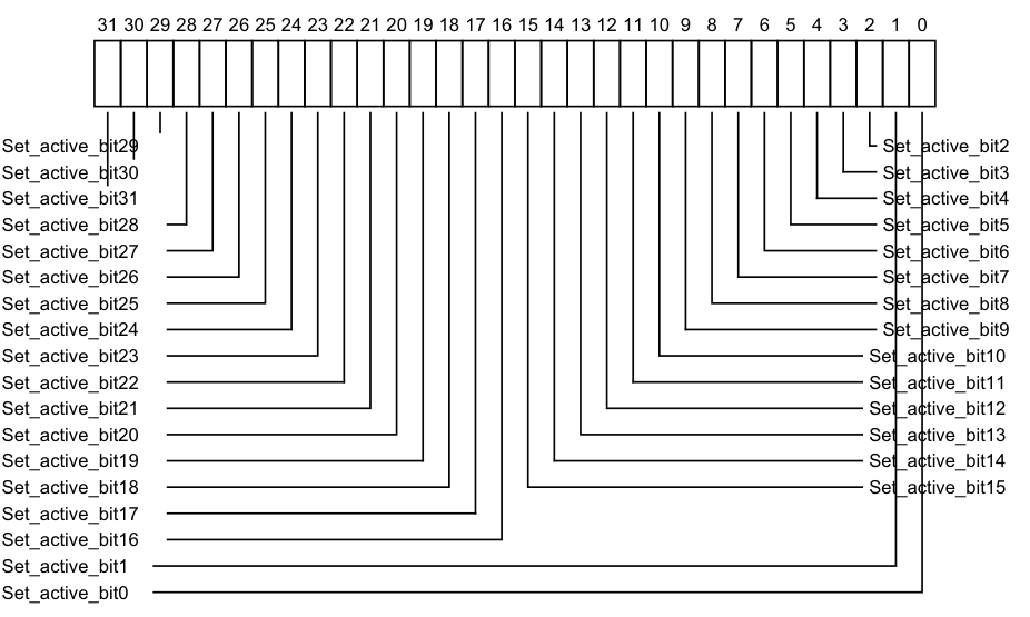
Image text
31 30 29 28 27 26 25 24 23 22 21 20 19 18 17 16 15 14 13 12 11 10 9 8 7 6 5 4 3 2 1 0
Set_active_bit29 Set_active_bit2
Set_active_bit30 Set_active_bit3
Set_active_bit31 Set_active_bit4
Set_active_bit28 Set_active_bit5
Set_active_bit27 Set_active_bit6
Set_active_bit26 Set_active_bit7
Set_active_bit25 Set_active_bit8
Set_active_bit24 Set_active_bit9
Set_active_bit23 Set_active_bit10
Set_active_bit22 Set_active_bit11
Set_active_bit21 Set_active_bit12
Set_active_bit20 Set_active_bit13
Set_active_bit19 Set_active_bit14
Set_active_bit18 Set_active_bit15
Set_active_bit17
Set_active_bit16
Set_active_bit1
Set_active_bit0
0b0 If read, indicates that the corresponding interrupt is not active, and is not active and pending.
If written, has no effect.
0b1 If read, indicates that the corresponding interrupt is active, or active and pending on this PE.
If written, activates the corresponding interrupt, if the interrupt is not already active. If the interrupt is already active, the write has no effect.
After a write of 1 to this bit, a subsequent read of this bit returns 1.
On a Warm reset, this field resets to an architecturally UNKNOWN value. For INTID m, when DIV and MOD are the integer division and modulo operations:
-
The corresponding GICR_ISACTIVER
E number, n, is given by n = (m-1024) DIV 32. -
The offset of the required GICR_ISACTIVER
E is (0x200 + (4*n)). -
The bit number of the required group modifier bit in this register is (m-1024) MOD 32.
Accessing the GICR_ISACTIVERE:
When affinity routing is not enabled for the Security state of an interrupt in GICR_ISACTIVER
When GICD_CTLR.DS==0, bits corresponding to Secure PPIs are RAZ/WI to Non-secure accesses.
Bits corresponding to unimplemented interrupts are RAZ/WI.
GICR_ISACTIVER
Component Frame Offset Instance
GIC Redistributor SGI_base 0x0300 + (4 * n) GICR_ISACTIVER
This interface is accessible as follows:
-
When GICD_CTLR.DS == 0 accesses to this register are RW.
-
When an access is Secure accesses to this register are RW.
-
When an access is Non-secure accesses to this register are RW.
12.11.23 GICR_ISENABLER0, Interrupt Set-Enable Register 0
The GICR_ISENABLER0 characteristics are:
Purpose
Enables forwarding of the corresponding SGI or PPI to the CPU interfaces.
Configurations
A copy of this register is provided for each Redistributor.
Attributes
GICR_ISENABLER0 is a 32-bit register.
Field descriptions
The GICR_ISENABLER0 bit assignments are:

Image text
31 30 29 28 27 26 25 24 23 22 21 20 19 18 17 16 15 14 13 12 11 10 9 8 7 6 5 4 3 2 1 0
Set_enable_bit29 Set_enable_bit2
Set_enable_bit30 Set_enable_bit3
Set_enable_bit31 Set_enable_bit4
Set_enable_bit28 Set_enable_bit5
Set_enable_bit27 Set_enable_bit6
Set_enable_bit26 Set_enable_bit7
Set_enable_bit25 Set_enable_bit8
Set_enable_bit24 Set_enable_bit9
Set_enable_bit23 Set_enable_bit10
Set_enable_bit22 Set_enable_bit11
Set_enable_bit21 Set_enable_bit12
Set_enable_bit20 Set_enable_bit13
Set_enable_bit19 Set_enable_bit14
Set_enable_bit18 Set_enable_bit15
Set_enable_bit17
Set_enable_bit16
Set_enable_bit1
Set_enable_bit0
0b0 If read, indicates that forwarding of the corresponding interrupt is disabled. If written, has no effect.
0b1 If read, indicates that forwarding of the corresponding interrupt is enabled. If written, enables forwarding of the corresponding interrupt. After a write of 1 to this bit, a subsequent read of this bit returns 1.
On a Warm reset, this field resets to 0.
Accessing the GICR_ISENABLER0:
When affinity routing is not enabled for the Security state of an interrupt in GICR_ISENABLER0, the corresponding bit is RAZ/WI and equivalent functionality is provided by GICD_ISENABLER
When GICD_CTLR.DS == 0, bits corresponding to Secure SGIs and PPIs are RAZ/WI to Non-secure accesses.
GICR_ISENABLER0 can be accessed through its memory-mapped interface:
| Component | Frame | Offset | Instance |
|---|---|---|---|
| GIC Redistributor | SGI_base | 0x0100 | GICR_ISENABLER0 |
This interface is accessible as follows:
-
When GICD_CTLR.DS == 0 accesses to this register are RW.
-
When an access is Secure accesses to this register are RW.
-
When an access is Non-secure accesses to this register are RW.
12.11.24 GICR_ISENABLERE, Interrupt Set-Enable Registers, n = 1 - 2
The GICR_ISENABLER
Purpose
Enables forwarding of the corresponding PPI to the CPU interfaces.
Configurations
This register is present only when FEAT_GICv3p1 is implemented. Otherwise, direct accesses to GICR_ISENABLER
A copy of this register is provided for each Redistributor.
Attributes
GICR_ISENABLER
Field descriptions
The GICR_ISENABLER

Image text
31 30 29 28 27 26 25 24 23 22 21 20 19 18 17 16 15 14 13 12 11 10 9 8 7 6 5 4 3 2 1 0
Set_enable_bit29 Set_enable_bit2
Set_enable_bit30 Set_enable_bit3
Set_enable_bit31 Set_enable_bit4
Set_enable_bit28 Set_enable_bit5
Set_enable_bit27 Set_enable_bit6
Set_enable_bit26 Set_enable_bit7
Set_enable_bit25 Set_enable_bit8
Set_enable_bit24 Set_enable_bit9
Set_enable_bit23 Set_enable_bit10
Set_enable_bit22 Set_enable_bit11
Set_enable_bit21 Set_enable_bit12
Set_enable_bit20 Set_enable_bit13
Set_enable_bit19 Set_enable_bit14
Set_enable_bit18 Set_enable_bit15
Set_enable_bit17
Set_enable_bit16
Set_enable_bit1
Set_enable_bit0
0b0 If read, indicates that forwarding of the corresponding interrupt is disabled. If written, has no effect.
0b1 If read, indicates that forwarding of the corresponding interrupt is enabled. If written, enables forwarding of the corresponding interrupt. After a write of 1 to this bit, a subsequent read of this bit returns 1.
On a Warm reset, this field resets to 0.
For INTID m, when DIV and MOD are the integer division and modulo operations:
-
The corresponding GICR_ISENABLER
E number, n, is given by n = (m-1024) DIV 32. -
The offset of the required GICR_ISENABLER
E is (0x100 + (4*n)). -
The bit number of the required group modifier bit in this register is (m-1024) MOD 32.
Accessing the GICR_ISENABLERE:
When affinity routing is not enabled for the Security state of an interrupt in GICR_ISENABLER
When GICD_CTLR.DS==0, bits corresponding to Secure PPIs are RAZ/WI to Non-secure accesses.
Bits corresponding to unimplemented interrupts are RAZ/WI.
GICR_ISENABLER
| Component | Frame | Offset | Instance |
|---|---|---|---|
| GIC Redistributor | SGI_base | 0x0100+ (4 * n) | GICR_ISENABLER |
This interface is accessible as follows:
-
When GICD_CTLR.DS == 0 accesses to this register are RW.
-
When an access is Secure accesses to this register are RW.
-
When an access is Non-secure accesses to this register are RW.
12.11.25 GICR_ISPENDR0, Interrupt Set-Pending Register 0
The GICR_ISPENDR0 characteristics are:
Purpose
Adds the pending state to the corresponding SGI or PPI.
Configurations
A copy of this register is provided for each Redistributor.
Attributes
GICR_ISPENDR0 is a 32-bit register.
Field descriptions
The GICR_ISPENDR0 bit assignments are:

Image text
31 30 29 28 27 26 25 24 23 22 21 20 19 18 17 16 15 14 13 12 11 10 9 8 7 6 5 4 3 2 1 0
Set_pending_bit29 Set_pending_bit2
Set_pending_bit30 Set_pending_bit3
Set_pending_bit31 Set_pending_bit4
Set_pending_bit28 Set_pending_bit5
Set_pending_bit27 Set_pending_bit6
Set_pending_bit26 Set_pending_bit7
Set_pending_bit25 Set_pending_bit8
Set_pending_bit24 Set_pending_bit9
Set_pending_bit23 Set_pending_bit10
Set_pending_bit22 Set_pending_bit11
Set_pending_bit21 Set_pending_bit12
Set_pending_bit20 Set_pending_bit13
Set_pending_bit19 Set_pending_bit14
Set_pending_bit18 Set_pending_bit15
Set_pending_bit17
Set_pending_bit16
Set_pending_bit1
Set_pending_bit0
-
0b0 If read, indicates that the corresponding interrupt is not pending on this PE. If written, has no effect.
-
0b1 If read, indicates that the corresponding interrupt is pending, or active and pending on this PE.
If written, changes the state of the corresponding interrupt from inactive to pending, or from active to active and pending. This has no effect in the following cases:
-
If the interrupt is already pending because of a write to GICR_ISPENDR0.
-
If the interrupt is already pending because the corresponding interrupt signal is asserted. In this case, the interrupt remains pending if the interrupt signal is deasserted.
On a Warm reset, this field resets to an architecturally UNKNOWN value.
Accessing the GICR_ISPENDR0:
When affinity routing is not enabled for the Security state of an interrupt in GICR_ISPENDR0, the corresponding bit is RAZ/WI and equivalent functionality is provided by GICD_ISPENDR
This register only applies to SGIs (bits [15:0]) and PPIs (bits [31:16]). For SPIs, this functionality is provided by GICD_ISPENDR
When GICD_CTLR.DS == 0, bits corresponding to Secure SGIs and PPIs are RAZ/WI to Non-secure accesses.
GICR_ISPENDR0 can be accessed through its memory-mapped interface:
| Component | Frame | Offset | Instance |
|---|---|---|---|
| GIC Redistributor | SGI_base | 0x0200 | GICR_ISPENDR0 |
This interface is accessible as follows:
-
When GICD_CTLR.DS == 0 accesses to this register are RW.
-
When an access is Secure accesses to this register are RW.
-
When an access is Non-secure accesses to this register are RW.
12.11.26 GICR_ISPENDRE, Interrupt Set-Pending Registers, n = 1 - 2
The GICR_ISPENDR
Purpose
Adds the pending state to the corresponding PPI.
Configurations
This register is present only when FEAT_GICv3p1 is implemented. Otherwise, direct accesses to GICR_ISPENDR
A copy of this register is provided for each Redistributor.
Attributes
GICR_ISPENDR
Field descriptions
The GICR_ISPENDR

Image text
31 30 29 28 27 26 25 24 23 22 21 20 19 18 17 16 15 14 13 12 11 10 9 8 7 6 5 4 3 2 1 0
Set_pending_bit29 Set_pending_bit2
Set_pending_bit30 Set_pending_bit3
Set_pending_bit31 Set_pending_bit4
Set_pending_bit28 Set_pending_bit5
Set_pending_bit27 Set_pending_bit6
Set_pending_bit26 Set_pending_bit7
Set_pending_bit25 Set_pending_bit8
Set_pending_bit24 Set_pending_bit9
Set_pending_bit23 Set_pending_bit10
Set_pending_bit22 Set_pending_bit11
Set_pending_bit21 Set_pending_bit12
Set_pending_bit20 Set_pending_bit13
Set_pending_bit19 Set_pending_bit14
Set_pending_bit18 Set_pending_bit15
Set_pending_bit17
Set_pending_bit16
Set_pending_bit1
Set_pending_bit0
-
0b0 If read, indicates that the corresponding interrupt is not pending on this PE. If written, has no effect.
-
0b1 If read, indicates that the corresponding interrupt is pending, or active and pending on this PE.
- If written, changes the state of the corresponding interrupt from inactive to pending, or from active to active and pending.
This has no effect in the following cases:
- If the interrupt is already pending because of a write to GICR_ISPENDR
E. - If the interrupt is already pending because the corresponding interrupt signal is asserted. In this case, the interrupt remains pending if the interrupt signal is deasserted.
On a Warm reset, this field resets to an architecturally UNKNOWN value.
For INTID m, when DIV and MOD are the integer division and modulo operations:
-
The corresponding GICR_ISPENDR
E number, n, is given by n = (m-1024) DIV 32. -
The offset of the required GICR_ISPENDR
E is (0x200 + (4*n)). -
The bit number of the required group modifier bit in this register is (m-1024) MOD 32.
Accessing the GICR_ISPENDRE:
When affinity routing is not enabled for the Security state of an interrupt in GICR_ISPENDR
When GICD_CTLR.DS==0, bits corresponding to Secure PPIs are RAZ/WI to Non-secure accesses.
Bits corresponding to unimplemented interrupts are RAZ/WI.
GICR_ISPENDR
Component Frame Offset Instance GIC Redistributor SGI_base 0x0200 + (4 * n) GICR_ISPENDR
This interface is accessible as follows:
-
When GICD_CTLR.DS == 0 accesses to this register are RW.
-
When an access is Secure accesses to this register are RW.
-
When an access is Non-secure accesses to this register are RW.
12.11.27 GICR_MPAMIDR, Report maximum PARTID and PMG Register
The GICR_MPAMIDR characteristics are:
Purpose
Reports the maximum support PARTID and PMG values.
Configurations
This register is present only when FEAT_GICv3p1 is implemented. Otherwise, direct accesses to GICR_MPAMIDR are RES0.
A copy of this register is provided for each Redistributor.
When GICR_TYPER.MPAM==0, this register is RES0.
Attributes
GICR_MPAMIDR is a 32-bit register.
Field descriptions
The GICR_MPAMIDR bit assignments are:

31 24 23 16 15 0
RES0 PMGmax PARTIDmax
Bits [31:24]
Reserved, RES0.
PMGmax, bits [23:16]
Maximum PMG value supported.
PARTIDmax, bits [15:0]
Maximum PARTID value supported.
Accessing the GICR_MPAMIDR:
GICR_MPAMIDR can be accessed through its memory-mapped interface:
Component Frame Offset Instance GIC Redistributor RD_base 0x0018 GICR_MPAMIDR
This interface is accessible as follows:
-
When GICD_CTLR.DS == 0 accesses to this register are RO.
-
When an access is Secure accesses to this register are RO.
-
When an access is Non-secure accesses to this register are RO.
12.11.28 GICR_NSACR, Non-secure Access Control Register
The GICR_NSACR characteristics are:
Purpose
Enables Secure software to permit Non-secure software to create SGIs targeting the PE connected to this Redistributor by writing to ICC_SGI1R_EL1, ICC_ASGI1R_EL1 or ICC_SGI0R_EL1. For more information, see Table 12-14.
Configurations
For a description on when a write to ICC_SGI0R_EL1, ICC_SGI1R_EL1 or ICC_ASGI1R_EL1 is permitted to generate an interrupt, see Use of control registers for SGI forwarding.
Attributes
GICR_NSACR is a 32-bit register.
Field descriptions
The GICR_NSACR bit assignments are:

Image text
31 30 29 28 27 26 25 24 23 22 21 20 19 18 17 16 15 14 13 12 11 10 9 8 7 6 5 4 3 2 1 0
NS_access15 NS_access1
NS_access14 NS_access2
NS_access13 NS_access3
NS_access12 NS_access4
NS_access11 NS_access5
NS_access10 NS_access6
NS_access9 NS_access7
NS_access8
NS_access0
0b00 Non-secure writes are not permitted to generate Secure Group 0 SGIs or Secure Group 1 SGIs. 0b01 Non-secure writes are permitted to generate a Secure Group 0 SGI. 0b10 As 0b01, but additionally Non-secure writes to are permitted to generate a Secure Group 1 SGI. 0b11 Reserved.
If the field is programmed to the reserved value, then the hardware will treat the field as if it has been programmed to an IMPLEMENTATION DEFINED choice of the valid values. However, to maintain the principle that as the value increases additional accesses are permitted Arm strongly recommends that implementations treat this value as 0b10. It is IMPLEMENTATION DEFINED whether the value read back is the value programmed or the valid value chosen.
On a Warm reset, this field resets to an architecturally UNKNOWN value.
Accessing the GICR_NSACR:
When GICD_CTLR.DS == 1, this register is RAZ/WI.
When GICD_CTLR.DS == 0, this register is Secure, and is RAZ/WI to Non-secure accesses.
This register is used when affinity routing is enabled. When affinity routing is not enabled for the Security state of the interrupt, GICD_NSACR
This register does not support PPIs.
GICR_NSACR can be accessed through its memory-mapped interface:
Component Frame Offset Instance GIC Redistributor SGI_base 0x0E00 GICR_NSACR
This interface is accessible as follows:
-
When GICD_CTLR.DS == 0 accesses to this register are RW.
-
When an access is Secure accesses to this register are RW.
-
When an access is Non-secure accesses to this register are RW.
12.11.29 GICR_PARTIDR, Set PARTID and PMG Register
The GICR_PARTIDR characteristics are:
Purpose
Sets the PARTID and PMG values used for memory accesses by the Redistributor.
Configurations
This register is present only when FEAT_GICv3p1 is implemented. Otherwise, direct accesses to GICR_PARTIDR are RES0.
A copy of this register is provided for each Redistributor.
When GICR_TYPER.MPAM==0, this register is RES0.
Attributes
GICR_PARTIDR is a 32-bit register.
Field descriptions
The GICR_PARTIDR bit assignments are:

31 24 23 16 15 0
RES0 PMG PARTID
Bits [31:24]
Reserved, RES0.
PMG, bits [23:16]
PMG value used when Redistributor accesses memory.
It is IMPLEMENTATION DEFINED whether bits not needed to represent PMG values in the range 0 to PMG_MAX are stateful or RES0.
On a Warm reset, this field resets to 0.
PARTID, bits [15:0]
PARTID value used when Redistributor accesses memory.
It is IMPLEMENTATION DEFINED whether bits not needed to represent PARTID values in the range 0 to PARTID_MAX are stateful or RES0.
On a Warm reset, this field resets to 0.
Accessing the GICR_PARTIDR:
GICR_PARTIDR can be accessed through its memory-mapped interface:
Component Frame Offset Instance GIC Redistributor RD_base 0x001C GICR_PARTIDR
This interface is accessible as follows:
-
When GICD_CTLR.DS == 0 accesses to this register are RW.
-
When an access is Secure accesses to this register are RW.
-
When an access is Non-secure accesses to this register are RW.
12.11.30 GICR_PENDBASER, Redistributor LPI Pending Table Base Address Register
The GICR_PENDBASER characteristics are:
Purpose
Specifies the base address of the LPI Pending table, and the Shareability and Cacheability of accesses to the LPI Pending table.
Configurations
A copy of this register is provided for each Redistributor.
Attributes
GICR_PENDBASER is a 64-bit register.
Field descriptions
The GICR_PENDBASER bit assignments are:
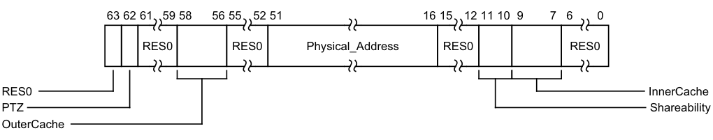
Image text
63 62 61 59 58 56 55 52 51 16 15 12 11 10 9 7 6 0
RES0 RES0 Physical_Address RES0 RES0
RES0 InnerCache
PTZ Shareability
OuterCache
PTZ, bit [62]
Pending Table Zero. Indicates to the Redistributor whether the LPI Pending table is zero when GICR_CTLR.EnableLPIs == 1.
This field is WO, and reads as 0.
0b0 The LPI Pending table is not zero, and contains live data.
0b1 The LPI Pending table is zero. Software must ensure the LPI Pending table is zero before this value is written.
Bits [61:59]
Reserved, RES0.
OuterCache, bits [58:56]
Indicates the Outer Cacheability attributes of accesses to the LPI Pending table. The possible values of this field are:
0b000 Memory type defined in InnerCache field. For Normal memory, Outer Cacheability is the same as Inner Cacheability.
0b001 Normal Outer Non-cacheable. 0b010 Normal Outer Cacheable Read-allocate, Write-through. 0b011 Normal Outer Cacheable Read-allocate, Write-back. 0b100 Normal Outer Cacheable Write-allocate, Write-through. 0b101 Normal Outer Cacheable Write-allocate, Write-back. 0b110 Normal Outer Cacheable Read-allocate, Write-allocate, Write-through. 0b111 Normal Outer Cacheable Read-allocate, Write-allocate, Write-back. It is IMPLEMENTATION DEFINED whether this field has a fixed value or can be programmed by software. Implementing this field with a fixed value is deprecated.
On a Warm reset, this field resets to an architecturally UNKNOWN value.
Bits [55:52]
Reserved, RES0.
Physical_Address, bits [51:16]
Bits [51:16] of the physical address containing the LPI Pending table.
In implementations supporting fewer than 52 bits of physical address, unimplemented upper bits are RES0. On a Warm reset, this field resets to an architecturally UNKNOWN value.
Bits [15:12]
Reserved, RES0.
Shareability, bits [11:10]
Indicates the Shareability attributes of accesses to the LPI Pending table. The possible values of this field are:
0b00 Non-shareable. 0b01 Inner Shareable. 0b10 Outer Shareable. 0b11 Reserved. Treated as 0b00.
It is IMPLEMENTATION DEFINED whether this field has a fixed value or can be programmed by software. Implementing this field with a fixed value is deprecated.
On a Warm reset, this field resets to an architecturally UNKNOWN value.
InnerCache, bits [9:7]
Indicates the Inner Cacheability attributes of accesses to the LPI Pending table. The possible values of this field are:
0b000 Device-nGnRnE. 0b001 Normal Inner Non-cacheable. 0b010 Normal Inner Cacheable Read-allocate, Write-through. 0b011 Normal Inner Cacheable Read-allocate, Write-back. 0b100 Normal Inner Cacheable Write-allocate, Write-through. 0b101 Normal Inner Cacheable Write-allocate, Write-back. 0b110 Normal Inner Cacheable Read-allocate, Write-allocate, Write-through. 0b111 Normal Inner Cacheable Read-allocate, Write-allocate, Write-back. On a Warm reset, this field resets to an architecturally UNKNOWN value.
Bits [6:0]
Reserved, RES0.
Accessing the GICR_PENDBASER:
Having the GICR_PENDBASER OuterCache, Shareability or InnerCache fields programmed to different values on different Redistributors with GICR_CTLR.EnableLPIs == 1 in the system is UNPREDICTABLE.
Changing GICR_PENDBASER with GICR_CTLR.EnableLPIs == 1 is UNPREDICTABLE. GICR_PENDBASER can be accessed through its memory-mapped interface:
| Component | Frame | Offset | Instance |
|---|---|---|---|
| GIC Redistributor | RD_base | 0x0078 | GICR_PENDBASER |
This interface is accessible as follows:
-
When GICD_CTLR.DS == 0 accesses to this register are RW.
-
When an access is Secure accesses to this register are RW.
-
When an access is Non-secure accesses to this register are RW.
12.11.31 GICR_PROPBASER, Redistributor Properties Base Address Register
The GICR_PROPBASER characteristics are:
Purpose
Specifies the base address of the LPI Configuration table, and the Shareability and Cacheability of accesses to the LPI Configuration table.
Configurations
A copy of this register is provided for each Redistributor.
An implementation might make this register RO, for example to correspond to an LPI Configuration table in read-only memory.
Attributes
GICR_PROPBASER is a 64-bit register.
Field descriptions
The GICR_PROPBASER bit assignments are:
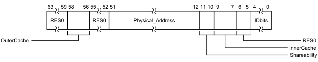
Image text
63 59 58 56 55 52 51 12 11 10 9 7 6 5 4 0
RES0 RES0 Physical_Address IDbits
OuterCache RES0
InnerCache
Shareability
Reserved, RES0. OuterCache, bits [58:56]
Indicates the Outer Cacheability attributes of accesses to the LPI Configuration table. The possible values of this field are: 0b000 Memory type defined in InnerCache field. For Normal memory, Outer Cacheability is the same as Inner Cacheability. 0b001 Normal Outer Non-cacheable. 0b010 Normal Outer Cacheable Read-allocate, Write-through. 0b011 Normal Outer Cacheable Read-allocate, Write-back. 0b100 Normal Outer Cacheable Write-allocate, Write-through. 0b101 Normal Outer Cacheable Write-allocate, Write-back. 0b110 Normal Outer Cacheable Read-allocate, Write-allocate, Write-through. 0b111 Normal Outer Cacheable Read-allocate, Write-allocate, Write-back. It is IMPLEMENTATION DEFINED whether this field has a fixed value or can be programmed by software. Implementing this field with a fixed value is deprecated.
On a Warm reset, this field resets to an architecturally UNKNOWN value.
Bits [55:52]
Reserved, RES0.
Physical_Address, bits [51:12]
Bits [51:12] of the physical address containing the LPI Configuration table. In implementations supporting fewer than 52 bits of physical address, unimplemented upper bits are RES0.
On a Warm reset, this field resets to an architecturally UNKNOWN value.
Shareability, bits [11:10]
Indicates the Shareability attributes of accesses to the LPI Configuration table. The possible values of this field are:
0b00 Non-shareable. 0b01 Inner Shareable. 0b10 Outer Shareable. 0b11 Reserved. Treated as 0b00.
It is IMPLEMENTATION DEFINED whether this field has a fixed value or can be programmed by software. Implementing this field with a fixed value is deprecated.
On a Warm reset, this field resets to an architecturally UNKNOWN value.
InnerCache, bits [9:7]
Indicates the Inner Cacheability attributes of accesses to the LPI Configuration table. The possible values of this field are:
0b000 Device-nGnRnE. 0b001 Normal Inner Non-cacheable. 0b010 Normal Inner Cacheable Read-allocate, Write-through. 0b011 Normal Inner Cacheable Read-allocate, Write-back. 0b100 Normal Inner Cacheable Write-allocate, Write-through. 0b101 Normal Inner Cacheable Write-allocate, Write-back. 0b110 Normal Inner Cacheable Read-allocate, Write-allocate, Write-through. 0b111 Normal Inner Cacheable Read-allocate, Write-allocate, Write-back. On a Warm reset, this field resets to an architecturally UNKNOWN value.
Bits [6:5]
Reserved, RES0.
IDbits, bits [4:0]
The number of bits of LPI INTID supported, minus one, by the LPI Configuration table starting at Physical_Address.
If the value of this field is larger than the value of GICD_TYPER.IDbits, the GICD_TYPER.IDbits value applies.
If the value of this field is less than 0b1101, indicating that the largest INTID is less than 8192 (the smallest LPI interrupt ID), the GIC will behave as if all physical LPIs are out of range.
On a Warm reset, this field resets to an architecturally UNKNOWN value.
Accessing the GICR_PROPBASER:
It is IMPLEMENTATION DEFINED whether GICR_PROPBASER can be set to different values on different Redistributors. GICR_TYPER.CommonLPIAff identifies the Redistributors that must have GICR_PROPBASER set to the same values whenever GICR_CTLR.EnableLPIs == 1.
Setting different values in different copies of GICR_PROPBASER on Redistributors that are required to use a common LPI Configuration table when GICR_CTLR.EnableLPIs == 1 leads to UNPREDICTABLE behavior.
Other restrictions apply when a Redistributor caches information from GICR_PROPBASER. For more information, see LPI Configuration tables. GICR_PROPBASER can be accessed through its memory-mapped interface:
| Component | Frame | Offset | Instance |
|---|---|---|---|
| GIC Redistributor | RD_base | 0x0070 | GICR_PROPBASER |
This interface is accessible as follows:
-
When GICD_CTLR.DS == 0 accesses to this register are RW.
-
When an access is Secure accesses to this register are RW.
-
When an access is Non-secure accesses to this register are RW.
12.11.32 GICR_SETLPIR, Set LPI Pending Register
The GICR_SETLPIR characteristics are:
Purpose
Generates an LPI by setting the pending state of the specified LPI.
Configurations
This register is present only when FEAT_GICv4p1 is implemented. Otherwise, direct accesses to GICR_SETLPIR are RES0.
A copy of this register is provided for each Redistributor.
Attributes
GICR_SETLPIR is a 64-bit register.
Field descriptions
The GICR_SETLPIR bit assignments are:
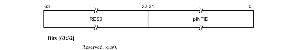
63 32 31 0
RES0 pINTID
Bits [63:32]
Reserved, RES0.
pINTID, bits [31:0]
The INTID of the physical LPI to be generated.
Note
The size of this field is IMPLEMENTATION DEFINED, and is specified by the GICD_TYPER.IDbits field. Unimplemented bits are RES0.
Accessing the GICR_SETLPIR:
When written with a 32-bit write the data is zero-extended to 64 bits.
This register is mandatory in an implementation that supports LPIs and does not include an ITS. The functionality is IMPLEMENTATION DEFINED in an implementation that does include an ITS.
Writes to this register have no effect if either:
-
The pINTID field corresponds to an LPI that is already pending.
-
The pINTID field corresponds to an unimplemented LPI.
-
GICR_CTLR.EnableLPIs == 0.
GICR_SETLPIR can be accessed through its memory-mapped interface:
Component Frame Offset Instance GIC Redistributor RD_base 0x0040 GICR_SETLPIR This interface is accessible as follows:
-
When GICD_CTLR.DS == 0 accesses to this register are WO.
-
When an access is Secure accesses to this register are WO.
-
When an access is Non-secure accesses to this register are WO.
12.11.33 GICR_STATUSR, Error Reporting Status Register
The GICR_STATUSR characteristics are:
Purpose
Provides software with a mechanism to detect:
-
Accesses to reserved locations.
-
Writes to read-only locations.
-
Reads of write-only locations.
Configurations
A copy of this register is provided for each Redistributor.
If the GIC implementation supports two Security states this register is Banked to provide Secure and Non-secure copies.
Attributes
GICR_STATUSR is a 32-bit register.
Field descriptions
The GICR_STATUSR bit assignments are:

Image text
31 4 3 2 1 0
RES0
RRD
WRD
RWOD
WROD
WROD, bit [3]
Write to an RO location. 0b0 Normal operation. 0b1 A write to an RO location has been detected.
When a violation is detected, software must write 1 to this register to reset it.
RWOD, bit [2]
Read of a WO location. 0b0 Normal operation. 0b1 A read of a WO location has been detected. When a violation is detected, software must write 1 to this register to reset it.
WRD, bit [1]
Write to a reserved location. 0b0 Normal operation. 0b1 A write to a reserved location has been detected. When a violation is detected, software must write 1 to this register to reset it.
RRD, bit [0]
Read of a reserved location.
0b0 Normal operation. 0b1 A read of a reserved location has been detected. When a violation is detected, software must write 1 to this register to reset it.
Accessing the GICR_STATUSR:
This is an optional register. If the register is not implemented, the location is RAZ/WI.
GICR_STATUSR can be accessed through its memory-mapped interface:
Component Frame Offset Instance GIC Redistributor RD_base 0x0010 GICR_STATUSR (S)
This interface is accessible as follows:
-
When GICD_CTLR.DS == 0 accesses to this register are RW.
-
When an access is Secure accesses to this register are RW.
GICR_STATUSR can be accessed through its memory-mapped interface:
| Component | Frame | Offset | Instance |
|---|---|---|---|
| GIC Redistributor | RD_base | 0x0010 | GICR_STATUSR (NS) |
This interface is accessible as follows:
-
When GICD_CTLR.DS == 0 accesses to this register are RW.
-
When an access is Non-secure accesses to this register are RW.
12.11.34 GICR_SYNCR, Redistributor Synchronize Register
The GICR_SYNCR characteristics are:
Purpose
Indicates completion of register based invalidate operations.
Configurations
A copy of this register is provided for each Redistributor.
Attributes
GICR_SYNCR is a 32-bit register.
Field descriptions
The GICR_SYNCR bit assignments are:

31 1 0
RES0
Busy
Bits [31:1]
Reserved, RES0.
Busy, bit [0]
Indicates completion of invalidation operations
0b0 No operations are in progress. 0b1 A write is in progress to one or more of the following registers: • GICR_INVLPIR. • GICR_INVALLR. • GICv3, GICR_CLRLPIR.
This field tracks operations initiated on the same Redistributor.
Accessing the GICR_SYNCR:
When this register is accessed, it is optional that an implementation might wait until all operations are complete before returning a value, in which case GICR_SYNCR.Busy is always 0.
This register is mandatory when any of the following are true:
-
GICR_TYPER.Direct is 1.
-
GICR_CTLR.IR is 1.
-
GICv4.1 is implemented.
Otherwise, the functionality is IMPLEMENTATION DEFINED.
GICR_SYNCR can be accessed through its memory-mapped interface:
Component Frame Offset Instance GIC Redistributor RD_base 0x00C0 GICR_SYNCR This interface is accessible as follows:
-
When GICD_CTLR.DS == 0 accesses to this register are RO.
-
When an access is Secure accesses to this register are RO.
-
When an access is Non-secure accesses to this register are RO.
12.11.35 GICR_TYPER, Redistributor Type Register
The GICR_TYPER characteristics are:
Purpose
Provides information about the configuration of this Redistributor.
Configurations
A copy of this register is provided for each Redistributor.
Attributes
GICR_TYPER is a 64-bit register.
Field descriptions
The GICR_TYPER bit assignments are:
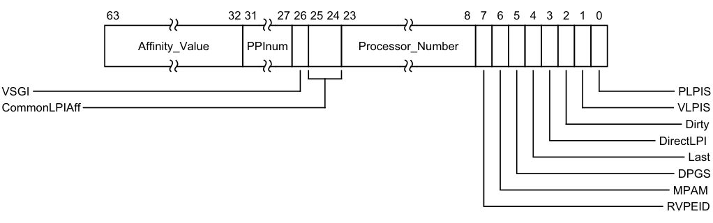
Image text
63 32 31 27 26 25 24 23 8 7 6 5 4 3 2 1 0
Affinity_Value PPInum Processor_Number
VSGI PLPIS
CommonLPIAff VLPIS
Dirty
DirectLPI
Last
DPGS
MPAM
RVPEID
Bits [63:56] provide Aff3, the Affinity level 3 value for the Redistributor. Bits [55:48] provide Aff2, the Affinity level 2 value for the Redistributor. Bits [47:40] provide Aff1, the Affinity level 1 value for the Redistributor. Bits [39:32] provide Aff0, the Affinity level 0 value for the Redistributor.
PPInum, bits [31:27]
When FEAT_GICv3p1 is implemented:
PPInum
The value derived from this field specifies the maximum PPI INTID that a GIC implementation can support. An implementation might not implement all PPIs up to this maximum.
0b00000 Maximum PPI INTID is 31. 0b00001 Maximum PPI INTID is 1087. 0b00010 Maximum PPI INTID is 1119. All other values are reserved.
Otherwise:
Reserved, RES0.
When FEAT_GICv3p1 is implemented:
PPInum
The value derived from this field specifies the maximum PPI INTID that a GIC implementation can support. An implementation might not implement all PPIs up to this maximum. 0b00000 Maximum PPI INTID is 31. 0b00001 Maximum PPI INTID is 1087. 0b00010 Maximum PPI INTID is 1119. All other values are reserved.
Otherwise:
Reserved, RES0.
VSGI, bit [26]
When FEAT_GICv4p1 is implemented:
VSGI Indicates whether vSGIs are supported. 0b0 Direct injection of SGIs not supported. 0b1 Direct injection of SGIs supported.
Otherwise:
Reserved, RES0.
When FEAT_GICv4p1 is implemented:
VSGI Indicates whether vSGIs are supported. 0b0 Direct injection of SGIs not supported. 0b1 Direct injection of SGIs supported.
Otherwise:
Reserved, RES0.
CommonLPIAff, bits [25:24]
The affinity level at which Redistributors share an LPI Configuration table.
0b00 All Redistributors must share an LPI Configuration table. 0b01 All Redistributors with the same Aff3 value must share an LPI Configuration table. 0b10 All Redistributors with the same Aff3.Aff2 value must share an LPI Configuration table. 0b11 All Redistributors with the same Aff3.Aff2.Aff1 value must share an LPI Configuration table.
Processor_Number, bits [23:8]
A unique identifier for the PE. When GITS_TYPER.PTA == 0, an ITS uses this field to identify the interrupt target.
When affinity routing is disabled for a Security state, this field indicates which GICD_ITARGETSR
RVPEID, bit [7]
When FEAT_GICv4p1 is implemented:
RVPEID Indicates how the resident vPE is specified. 0b0 GICR_VPENDBASER records the address of the vPE’s Virtual Pending Table. 0b1 GICR_VPENDBASER records vPEID.
Otherwise:
Reserved, RES0.
When FEAT_GICv4p1 is implemented: RVPEID Indicates how the resident vPE is specified. 0b0 GICR_VPENDBASER records the address of the vPE’s Virtual Pending Table. 0b1 GICR_VPENDBASER records vPEID. Otherwise:
Reserved, RES0.
MPAM, bit [6]
When FEAT_GICv3p1 is implemented:
MPAM MPAM 0b0 MPAM not supported. 0b1 MPAM supported. Otherwise:
Reserved, RES0.
When FEAT_GICv3p1 is implemented: MPAM MPAM 0b0 MPAM not supported. 0b1 MPAM supported. Otherwise: Reserved, RES0.
DPGS, bit [5]
Sets support for GICR_CTLR.DPG* bits. 0b0 GICR_CTLR.DPG* bits are not supported. 0b1 GICR_CTLR.DPG* bits are supported. Last, bit [4]
Indicates whether this Redistributor is the highest-numbered Redistributor in a series of contiguous Redistributor pages.
0b0 This Redistributor is not the highest-numbered Redistributor in a series of contiguous Redistributor pages. 0b1 This Redistributor is the highest-numbered Redistributor in a series of contiguous Redistributor pages.
DirectLPI, bit [3]
Indicates whether this Redistributor supports direct injection of LPIs.
Dirty, bit [2]
0b0 This Redistributor does not support direct injection of LPIs. The GICR_SETLPIR, GICR_CLRLPIR, GICR_INVLPIR, GICR_INVALLR, and GICR_SYNCR registers are either not implemented, or have an IMPLEMENTATION DEFINED purpose. 0b1 This Redistributor supports direct injection of LPIs. The GICR_SETLPIR, GICR_CLRLPIR, GICR_INVLPIR, GICR_INVALLR, and GICR_SYNCR registers are implemented. Controls the functionality of GICR_VPENDBASER.Dirty.GICR_VPENDBASER.Dirty..Dirty. 0b0 GICR_VPENDBASER.Dirty is UNKNOWN when GICR_VPENDBASER.Valid == 1. 0b1 GICR_VPENDBASER.Dirty indicates when the Virtual Pending Table has been parsed when GICR_VPENDBASER.Valid is written from 0 to 1.
Controls the functionality of GICR_VPENDBASER.Dirty.GICR_VPENDBASER.Dirty..Dirty.
When GICR_TYPER.VLPIS == 0, this field is RES0.
Note In GICv4p1 implementations this field is RES1.
VLPIS, bit [1]
Indicates whether the GIC implementation supports virtual LPIs and the direct injection of virtual LPIs. 0b0 The implementation does not support virtual LPIs or the direct injection of virtual LPIs. 0b1 The implementation supports virtual LPIs and the direct injection of virtual LPIs.
Note In GICv3 implementations this field is RES0.
PLPIS, bit [0]
Indicates whether the GIC implementation supports physical LPIs.
0b0 The implementation does not support physical LPIs. 0b1 The implementation supports physical LPIs.
Accessing the GICR_TYPER:
GICR_TYPER can be accessed through its memory-mapped interface:
Component Frame Offset Instance GIC Redistributor RD_base 0x0008 GICR_TYPER
This interface is accessible as follows:
-
When GICD_CTLR.DS == 0 accesses to this register are RO.
-
When an access is Secure accesses to this register are RO.
-
When an access is Non-secure accesses to this register are RO.
12.11.36 GICR_VPENDBASER, Virtual Redistributor LPI Pending Table Base Address Register
The GICR_VPENDBASER characteristics are:
Purpose
Specifies the base address of the memory that holds the virtual LPI Pending table for the currently scheduled virtual machine.
Configurations
There are no configuration notes.
Attributes
GICR_VPENDBASER is a 64-bit register.
Field descriptions
The GICR_VPENDBASER bit assignments are:
When FEAT_GICv4 is implemented:
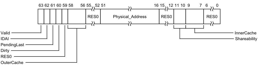
Image text
63 62 61 60 59 58 56 55 52 51 16 15 12 11 10 9 7 6 0
RES0 Physical_Address RES0 RES0
Valid InnerCache
IDAI Shareability
PendingLast
Dirty
RES0
OuterCache
| 0b0 | The virtual LPI Pending table is not valid. No vPE is scheduled. |
|---|---|
| 0b1 | The virtual LPI Pending table is valid. A vPE is scheduled. |
| Setting | GICR_VPENDBASER.Valid == 1 when the associated CPU interface does not implement |
| FEAT_GICv4 isUNPREDICTABLE. |
Note Software can determine whether a PE supports FEAT_GICv3 or FEAT_GICv4 by reading ID_AA64PFR0_EL1. Writing a new value to any bit of GICR_VPENDBASER, other than GICR_VPENDBASER.Valid, when GICR_VPENDBASER.Valid==1 is UNPREDICTABLE.
On a Warm reset, this field resets to 0.
IDAI, bit [62]
Implementation Defined Area Invalid. Indicates whether the IMPLEMENTATION DEFINED area in the virtual LPI Pending table is valid.
| 0b0 | TheIMPLEMENTATION DEFINEDarea is valid. |
|---|---|
| 0b1 | TheIMPLEMENTATION DEFINEDarea is invalid and all pending interrupt information is held in the architecturally defined part of the virtual LPI Pending table. |
For more information, see LPI Pending tables and Virtual LPI Configuration tables and virtual LPI Pending tables. On a Warm reset, this field resets to an architecturally UNKNOWN value.
PendingLast, bit [61]
Indicates whether there are pending and enabled interrupts for the last scheduled vPE.
This value is set by the implementation when GICR_VPENDBASER.Valid has been written from 1 to 0 and is otherwise UNKNOWN.
0b0 There are no pending and enabled interrupts for the last scheduled vPE. 0b1 There is at least one pending interrupt for the last scheduled vPE. It is IMPLEMENTATION DEFINED whether this bit is set when the only pending interrupts for the last scheduled vPE are not enabled. Arm deprecates setting PendingLast to 1 when the only pending interrupts for the last scheduled virtual machine are not enabled. When the GICR_VPENDBASER.Valid bit is written from 0 to 1, this bit is RES1.
On a Warm reset, this field resets to 0.
Dirty, bit [60]
When GICR_VPENDBASER.Valid == 0:
Dirty Indicates whether a de-scheduling operation is in progress. This field is read-only. 0b0 No de-scheduling operation in process. 0b1 De-scheduling operation in process. Writing 1 to GICR_VPENDBASER.Valid is UNPREDICTABLE while GICR_VPENDBASER.Dirty==1.
On a Warm reset, this field resets to 0.
When GICR_VPENDBASER.Valid == 1 and GICR_TYPER.Dirty == 1:
Dirty
This field is read-only. Reports whether the Virtual Pending table has been parsed.
0b0 Parsing of the Virtual Pending Table has completed. 0b1 Parsing of the Virtual Pending Table has not completed. Writing 1 to GICR_VPENDBASER.Valid is UNPREDICTABLE while GICR_VPENDBASER.Dirty == 1. On a Warm reset, this field resets to 0.
Otherwise:
Dirty This field is read-only. This fields is UNKNOWN. On a Warm reset, this field resets to 0.
When GICR_VPENDBASER.Valid == 0:
Dirty
Indicates whether a de-scheduling operation is in progress. This field is read-only.
0b0 No de-scheduling operation in process. 0b1 De-scheduling operation in process. Writing 1 to GICR_VPENDBASER.Valid is UNPREDICTABLE while GICR_VPENDBASER.Dirty==1.
On a Warm reset, this field resets to 0.
When GICR_VPENDBASER.Valid == 1 and GICR_TYPER.Dirty == 1:
Dirty
This field is read-only. Reports whether the Virtual Pending table has been parsed. 0b0 Parsing of the Virtual Pending Table has completed. 0b1 Parsing of the Virtual Pending Table has not completed. Writing 1 to GICR_VPENDBASER.Valid is UNPREDICTABLE while GICR_VPENDBASER.Dirty == 1.
On a Warm reset, this field resets to 0. Otherwise:
Dirty This field is read-only. This fields is UNKNOWN. On a Warm reset, this field resets to 0.
When GICR_VPENDBASER.Valid == 0:
Dirty
Indicates whether a de-scheduling operation is in progress. This field is read-only.
0b0 No de-scheduling operation in process. 0b1 De-scheduling operation in process. Writing 1 to GICR_VPENDBASER.Valid is UNPREDICTABLE while GICR_VPENDBASER.Dirty==1.
On a Warm reset, this field resets to 0.
When GICR_VPENDBASER.Valid == 1 and GICR_TYPER.Dirty == 1:
Dirty
This field is read-only. Reports whether the Virtual Pending table has been parsed.
0b0 Parsing of the Virtual Pending Table has completed. 0b1 Parsing of the Virtual Pending Table has not completed. Writing 1 to GICR_VPENDBASER.Valid is UNPREDICTABLE while GICR_VPENDBASER.Dirty == 1.
On a Warm reset, this field resets to 0.
Otherwise:
Dirty
This field is read-only. This fields is UNKNOWN.
On a Warm reset, this field resets to 0.
Bit [59]
Reserved, RES0.
OuterCache, bits [58:56]
Indicates the Outer Cacheability attributes of accesses to virtual LPI Pending tables of vPEs targeting this Redistributor.
0b000 Memory type defined in InnerCache field. For Normal memory, Outer Cacheability is the same as Inner Cacheability.
0b001 Normal Outer Non-cacheable. 0b010 Normal Outer Cacheable Read-allocate, Write-through. 0b011 Normal Outer Cacheable Read-allocate, Write-back. 0b100 Normal Outer Cacheable Write-allocate, Write-through. 0b101 Normal Outer Cacheable Write-allocate, Write-back. 0b110 Normal Outer Cacheable Read-allocate, Write-allocate, Write-through. 0b111 Normal Outer Cacheable Read-allocate, Write-allocate, Write-back.
It is IMPLEMENTATION DEFINED whether this field has a fixed value or can be programmed by software. Implementing this field with a fixed value is deprecated.
The Cacheability, Outer Cacheability and Shareability fields are used for accesses to the virtual LPI Pending table of resident and non-resident vPEs.
If the OuterCacheabilty attribute of the virtual LPI Pending tables that are associated with vPEs targeting the same Redistributor are different, behavior is UNPREDICTABLE.
On a Warm reset, this field resets to an architecturally UNKNOWN value.
Bits [55:52]
Reserved, RES0.
Physical_Address, bits [51:16]
Bits [51:16] of the physical address containing the virtual LPI Pending table.
In implementations supporting fewer than 52 bits of physical address, unimplemented upper bits are RES0.
On a Warm reset, this field resets to an architecturally UNKNOWN value.
Bits [15:12]
Reserved, RES0.
Shareability, bits [11:10]
Indicates the Shareability attributes of accesses to the virtual LPI Pending table.
0b00 Non-shareable. 0b01 Inner Shareable. 0b10 Outer Shareable. 0b11 Reserved. Treated as 0b00.
It is IMPLEMENTATION DEFINED whether this field has a fixed value or can be programmed by software. Implementing this field with a fixed value is deprecated.
The Cacheability, Outer Cacheability and Shareability fields are used for accesses to the virtual LPI Pending table of resident and non-resident vPEs.
If the Shareability attribute of the virtual LPI Pending tables that are associated with vPEs targeting the same Redistributor are different, behavior is UNPREDICTABLE.
On a Warm reset, this field resets to an architecturally UNKNOWN value.
InnerCache, bits [9:7]
Indicates the Inner Cacheability attributes of accesses to the virtual LPI Pending table.
0b000 Device-nGnRnE. 0b001 Normal Inner Non-cacheable. 0b010 Normal Inner Cacheable Read-allocate, Write-through. 0b011 Normal Inner Cacheable Read-allocate, Write-back. 0b100 Normal Inner Cacheable Write-allocate, Write-through. 0b101 Normal Inner Cacheable Write-allocate, Write-back. 0b110 Normal Inner Cacheable Read-allocate, Write-allocate, Write-through. 0b111 Normal Inner Cacheable Read-allocate, Write-allocate, Write-back.
The Cacheability, Outer Cacheability and Shareability fields are used for accesses to the virtual LPI Pending table of resident and non-resident vPEs. If the InnerCacheabilty attribute of the virtual LPI Pending tables that are associated with vPEs targeting the same Redistributor are different, behavior is UNPREDICTABLE.
On a Warm reset, this field resets to an architecturally UNKNOWN value.
Bits [6:0]
Reserved, RES0.
When FEAT_GICv4p1 is implemented:
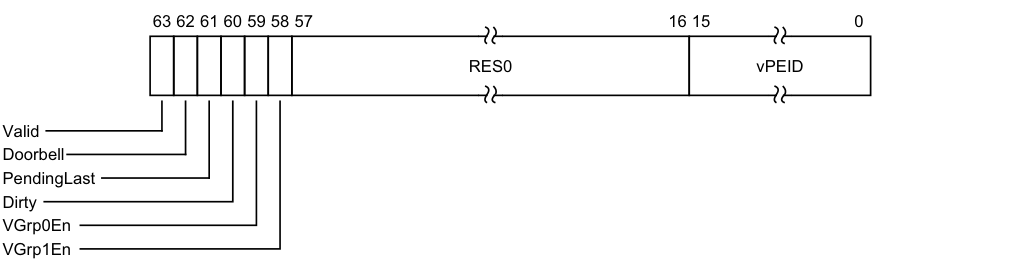
Image text
63 62 61 60 59 58 57 16 15 0
RES0 vPEID
Valid
Doorbell
PendingLast
Dirty
VGrp0En
VGrp1En
0b0 The virtual LPI Pending table is not valid. No vPE is scheduled.
0b1 The virtual LPI Pending table is valid. A vPE is scheduled.
Setting GICR_VPENDBASER.Valid == 1 when the associated CPU interface does not implement FEAT_GICv4 is UNPREDICTABLE.
Note Software can determine whether a PE supports FEAT_GICv3 or FEAT_GICv4 by reading ID_AA64PFR0_EL1.
Writing a new value to any bit of GICR_VPENDBASER, other than GICR_VPENDBASER.Valid, when GICR_VPENDBASER.Valid==1 is UNPREDICTABLE.
Setting GICR_VPENDBASER.Valid to 1 is UNPREDICTABLE if GICR_VPROPBASER.Valid == 0. On a Warm reset, this field resets to 0.
Doorbell, bit [62]
When GICR_VPENDBASER.Valid is written from 1 to 0, this bit controls whether a default doorbell interrupt is requested for the descheduled vPE.
0b0 No default doorbell requested.
0b1 Default doorbell requested.
When GICR_VPENDBASER.Valid is written from 1 to 0, if there are outstanding enabled pending interrupts then this bit is treated as 0.
When GICR_VPENDBASER.Valid is written from 1 to 0, if GICR_VPENDBASER.PendingLast is written as 1 then this bit is treated as 0.
When GICR_VPENDBASER.Valid == 1, reads return an UNKNOWN value.
On a Warm reset, this field resets to an UNKNOWN value.
PendingLast, bit [61]
Indicates whether there are pending and enabled interrupts for the last scheduled vPE. This value is set by the implementation when GICR_VPENDBASER.Valid is written from 1 to 0 and is otherwise UNKNOWN.
0b0 There are no pending and enabled interrupts for the last scheduled vPE. 0b1 There is at least one pending and enabled interrupt for the last scheduled vPE. When the GICR_VPENDBASER.Valid bit is written from 0 to 1, this bit is RES1. When GICR_VPENDBASER.Valid is written from 1 to 0, if GICR_VPENDBASER.PendingLast is written as 1, then this bit is set to an UNKNOWN value.
On a Warm reset, this field resets to an UNKNOWN value.
Dirty, bit [60]
When GICR_VPENDBASER.Valid == 0:
Dirty Read-only. Indicates whether a de-scheduling operation is in progress. 0b0 No de-scheduling operation in progess. 0b1 De-scheduling operation in progess. Writing 1 to GICR_VPENDBASER.Valid is UNPREDICTABLE while GICR_VPENDBASER.Dirty == 1. On a Warm reset, this field resets to 0. Otherwise:
Dirty Read-only. Reports whether the Virtual Pending table has been parsed. 0b0 Parsing of the Virtual Pending Table is complete. 0b1 Parsing of the Virtual Pending Table has not completed. Writing 1 to GICR_VPENDBASER.Valid is UNPREDICTABLE while GICR_VPENDBASER.Dirty == 1.
On a Warm reset, this field resets to 0.
When GICR_VPENDBASER.Valid == 0:
Dirty Read-only. Indicates whether a de-scheduling operation is in progress. 0b0 No de-scheduling operation in progess. 0b1 De-scheduling operation in progess. Writing 1 to GICR_VPENDBASER.Valid is UNPREDICTABLE while GICR_VPENDBASER.Dirty == 1. On a Warm reset, this field resets to 0.
Otherwise:
Dirty Read-only. Reports whether the Virtual Pending table has been parsed. 0b0 Parsing of the Virtual Pending Table is complete. 0b1 Parsing of the Virtual Pending Table has not completed. Writing 1 to GICR_VPENDBASER.Valid is UNPREDICTABLE while GICR_VPENDBASER.Dirty == 1. On a Warm reset, this field resets to 0.
VGrp0En, bit [59]
Enable virtual Group 0 interrupts. 0b0 Forwarding of virtual Group 0 interrupts disabled. 0b1 Forwarding of virtual Group 0 interrupts enabled.
Writing a new value to VGrp0En while GICR_VPENDBASER.Valid==1 is CONSTRAINED UNPREDICTABLE:
-
The update is ignored.
-
The update is ignored for all purposes other than a direct read of the register.
-
The virtual group enable is updated.
On a Warm reset, this field resets to an UNKNOWN value.
VGrp1En, bit [58]
Enable virtual Group 1 interrupts.
0b0 Forwarding of virtual Group 1 interrupts disabled. 0b1 Forwarding of virtual Group 1 interrupts enabled.
Writing a new value to VGrp1En while GICR_VPENDBASER.Valid==1 is CONSTRAINED UNPREDICTABLE:
-
The update is ignored.
-
The update is ignored for all purposes other than a direct read of the register.
-
The virtual group enable is updated.
On a Warm reset, this field resets to an UNKNOWN value.
Bits [57:16]
Reserved, RES0.
vPEID, bits [15:0]
When GICR_VPENDBASER.Valid == 1, ID of scheduled vPE.
When GICR_VPENDBASER.Valid == 1, if GICR_VPENDBASER.vPEID is set to a value greater than the configured vPEID width, the behavior of this field is CONSTRAINED UNPREDICTABLE:
-
GICR_VPENDBASER.vPEID is treated as having an UNKNOWN valid value for all purposes other than a direct read of the register.
-
GICR_VPENDBASER.Valid is treated as being set to 0 for all purposes other than a direct read of the register.
The size of this field is IMPLEMENTATION DEFINED, and is specified by the GICD_TYPER2.VIL and GICD_TYPER2.VID fields, unimplemented bits are RES0.
Accessing the GICR_VPENDBASER:
The effect of a write to this register is not guaranteed to be visible throughout the affinity hierarchy, as indicated by GICR_CTLR.RWP == 0.
GICR_VPENDBASER can be accessed through its memory-mapped interface:
| Component | Frame | Offset | Instance |
|---|---|---|---|
| GIC Redistributor | VLPI_base | 0x0078 | GICR_VPENDBASER |
This interface is accessible as follows:
-
When GICD_CTLR.DS == 0 accesses to this register are RW.
-
When an access is Secure accesses to this register are RW.
-
When an access is Non-secure accesses to this register are RW.
12.11.37 GICR_VPROPBASER, Virtual Redistributor Properties Base Address Register
The GICR_VPROPBASER characteristics are:
Purpose
Specifies the base address of the memory that holds the virtual LPI Configuration table for the currently scheduled virtual machine.
Configurations
This register is provided in FEAT_GICv4 implementations only.
Attributes
GICR_VPROPBASER is a 64-bit register.
Field descriptions
The GICR_VPROPBASER bit assignments are:
When FEAT_GICv4 is implemented:
OuterCache
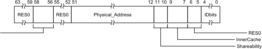
Image text
63 59 58 56 55 52 51 12 11 10 9 7 6 5 4 0
RES0 RES0 Physical_Address IDbits
RES0
InnerCache
Shareability
OuterCache, bits [58:56]
Indicates the Outer Cacheability attributes of accesses to the LPI Configuration table. The possible values of this field are:
0b000 Memory type defined in InnerCache field. For Normal memory, Outer Cacheability is the same as Inner Cacheability.
0b001 Normal Outer Non-cacheable. 0b010 Normal Outer Cacheable Read-allocate, Write-through. 0b011 Normal Outer Cacheable Read-allocate, Write-back. 0b100 Normal Outer Cacheable Write-allocate, Write-through. 0b101 Normal Outer Cacheable Write-allocate, Write-back. 0b110 Normal Outer Cacheable Read-allocate, Write-allocate, Write-through. 0b111 Normal Outer Cacheable Read-allocate, Write-allocate, Write-back.
It is IMPLEMENTATION DEFINED whether this field has a fixed value or can be programmed by software. Implementing this field with a fixed value is deprecated.
On a Warm reset, this field resets to an architecturally UNKNOWN value.
Bits [55:52]
Reserved, RES0.
Physical_Address, bits [51:12]
Bits [51:12] of the physical address containing the virtual LPI Configuration table. In implementations supporting fewer than 52 bits of physical address, unimplemented upper bits are RES0.
On a Warm reset, this field resets to an architecturally UNKNOWN value.
Shareability, bits [11:10]
Indicates the Shareability attributes of accesses to the LPI Configuration table. The possible values of this field are:
0b00 Non-shareable. 0b01 Inner Shareable. 0b10 Outer Shareable. 0b11 Reserved. Treated as 0b00.
It is IMPLEMENTATION DEFINED whether this field has a fixed value or can be programmed by software. Implementing this field with a fixed value is deprecated.
On a Warm reset, this field resets to an architecturally UNKNOWN value.
InnerCache, bits [9:7]
Indicates the Inner Cacheability attributes of accesses to the LPI Configuration table. The possible values of this field are:
0b000 Device-nGnRnE. 0b001 Normal Inner Non-cacheable. 0b010 Normal Inner Cacheable Read-allocate, Write-through. 0b011 Normal Inner Cacheable Read-allocate, Write-back. 0b100 Normal Inner Cacheable Write-allocate, Write-through. 0b101 Normal Inner Cacheable Write-allocate, Write-back. 0b110 Normal Inner Cacheable Read-allocate, Write-allocate, Write-through. 0b111 Normal Inner Cacheable Read-allocate, Write-allocate, Write-back.
On a Warm reset, this field resets to an architecturally UNKNOWN value.
Bits [6:5]
Reserved, RES0.
IDbits, bits [4:0]
The number of bits of virtual LPI INTID supported, minus one.
If the value of this field is less than 0b1101, indicating that the largest INTID is less than 8192 (the smallest LPI interrupt ID), the GIC will behave as if all virtual LPIs are out of range.
On a Warm reset, this field resets to an architecturally UNKNOWN value.
When FEAT_GICv4p1 is implemented:
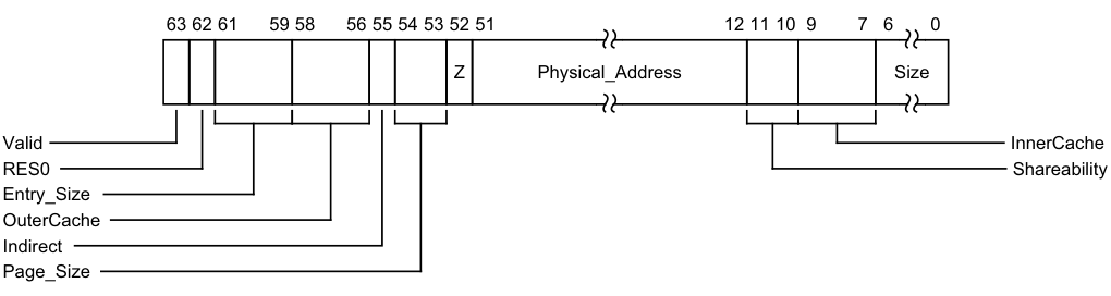
Image text
63 62 61 59 58 56 55 54 53 52 51 12 11 10 9 7 6 0
Z Physical_Address Size
Valid InnerCache
RES0 Shareability
Entry_Size
OuterCache
Indirect
Page_Size## Valid, bit [63]
This bit controls whether the vPE Configuration Table is valid:
0b0 The vPE Configuration table is not valid. 0b1 The vPE Configuration table is valid. TBC On a Warm reset, this field resets to 0.
Bit [62]
Reserved, RES0.
Entry_Size, bits [61:59]
Specifies the number of bytes per table entry, minus one.
This bit is read-only.
OuterCache, bits [58:56]
Indicates the Outer Cacheability attributes of accesses to the table. The possible values of this field are:
0b000 Memory type defined in InnerCache field. For Normal memory, Outer Cacheability is the same as Inner Cacheability. 0b001 Normal Outer Non-cacheable. 0b010 Normal Outer Cacheable Read-allocate, Write-through. 0b011 Normal Outer Cacheable Read-allocate, Write-back. 0b100 Normal Outer Cacheable Write-allocate, Write-through. 0b101 Normal Outer Cacheable Write-allocate, Write-back. 0b110 Normal Outer Cacheable Read-allocate, Write-allocate, Write-through. 0b111 Normal Outer Cacheable Read-allocate, Write-allocate, Write-back.
It is IMPLEMENTATION DEFINED whether this field has a fixed value or can be programmed by software. Implementing this field with a fixed value is deprecated.
On a Warm reset, this field resets to an UNKNOWN value.
Indirect, bit [55]
This field indicates whether GICR_VPROPBASER specifies a single, flat table or a two-level table where the first level contains a list of descriptors.
0b0 Single Level. The Size field indicates the number of pages used to store data associated with each table entry.
0b1 Two Level. The Size field indicates the number of pages that contain an array of 64-bit descriptors to pages that are used to store the data associated with each table entry. A little endian memory order model is used.
This field is RES0 for GIC implementations that only support flat tables.
On a Warm reset, this field resets to an UNKNOWN value.
Page_Size, bits [54:53]
The following values indicate the size of page that the translation table uses:
0b00 4KB. 0b01 16KB. 0b10 64KB. 0b11 Reserved. Treated as 0b10.
Note If the GIC implementation supports only a single, fixed page size, this field might be RO.
On a Warm reset, this field resets to an UNKNOWN value.
Z, bit [52]
When GICR_VPROPBASER.Valid is written from 0 to 1, GICR_VPROPBASER.Z indicates whether the vPE Configuration table is known to contain all zeros.
0b0 The vPE Configutation table is not zero, and contains live data. 0b1 The vPE Configuration table is zero. Setting GICR_VPROPBASER.Z to 0 causes the IRI to reload configuration from memory When GICR_VPROPBASER.Valid is written from 0 to 1, if GICR_VPROPBASER.Z==1 behavior is UNPREDICTABLE if the allocated memory does not contain all zeros.
This field is WO, and reads as 0.
Physical_Address, bits [51:12]
Bits [51:12] of the physical address containing the LPI Configuration table.
In implementations supporting fewer than 52 bits of physical address, unimplemented upper bits are RES0.
On a Warm reset, this field resets to an UNKNOWN value.
Shareability, bits [11:10]
Indicates the Shareability attributes of accesses to the LPI Configuration table. The possible values of this field are:
0b00 Non-shareable. 0b01 Inner Shareable. 0b10 Outer Shareable. 0b11 Reserved. Treated as 0b00.
It is IMPLEMENTATION DEFINED whether this field has a fixed value or can be programmed by software. Implementing this field with a fixed value is deprecated.
On a Warm reset, this field resets to an UNKNOWN value.
InnerCache, bits [9:7]
Indicates the Inner Cacheability attributes of accesses to the LPI Configuration table. The possible values of this field are:
0b000 Device-nGnRnE. 0b001 Normal Inner Non-cacheable. 0b010 Normal Inner Cacheable Read-allocate, Write-through. 0b011 Normal Inner Cacheable Read-allocate, Write-back. 0b100 Normal Inner Cacheable Write-allocate, Write-through. 0b101 Normal Inner Cacheable Write-allocate, Write-back. 0b110 Normal Inner Cacheable Read-allocate, Write-allocate, Write-through. 0b111 Normal Inner Cacheable Read-allocate, Write-allocate, Write-back.
On a Warm reset, this field resets to an UNKNOWN value.
Size, bits [6:0]
The number of pages of physical memory allocated to the table, minus one.
GICR_VPROPBASER.Page_Size specifies the size of each page.
On a Warm reset, this field resets to an UNKNOWN value.
Accessing the GICR_VPROPBASER:
GICR_VPROPBASER can be accessed through its memory-mapped interface:
| Component | Frame | Offset | Instance |
|---|---|---|---|
| GIC Redistributor | VLPI_base | 0x0070 | GICR_VPROPBASER |
This interface is accessible as follows:
-
When GICD_CTLR.DS == 0 accesses to this register are RW.
-
When an access is Secure accesses to this register are RW.
-
When an access is Non-secure accesses to this register are RW.
12.11.38 GICR_VSGIPENDR, Redistributor virtual SGI pending state register
The GICR_VSGIPENDR characteristics are:
Purpose
Requests the pending state of virtual SGIs for a specified vPE.
Configurations
This register is present only when FEAT_GICv4p1 is implemented. Otherwise, direct accesses to GICR_VSGIPENDR are RES0.
A copy of this register is provided for each Redistributor.
Attributes
GICR_VSGIPENDR is a 32-bit register.
Field descriptions
The GICR_VSGIPENDR bit assignments are:
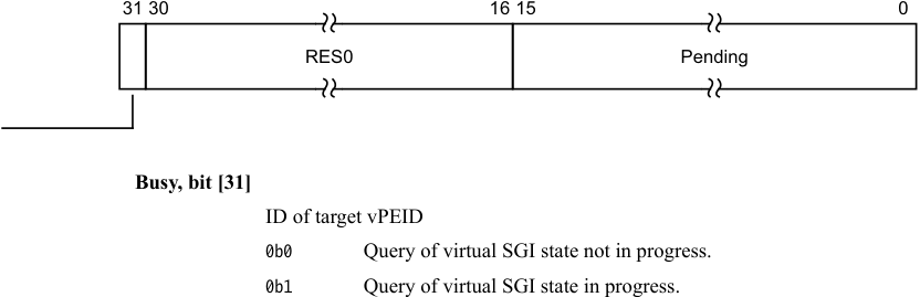
Image text
31 30 16 15 0
RES0 Pending
Busy, bit [31]
ID of target vPEID
0b0 Query of virtual SGI state not in progress.
0b1 Query of virtual SGI state in progress.
Busy
Bits [30:16]
Reserved, RES0.
Pending, bits [15:0]
Pending state of virtual SGIs for requested vPEID.
This field is UNKNOWN when GICR_VSGIPENDR.Busy == 1
Accessing the GICR_VSGIPENDR:
64-bit access only.
GICR_VSGIPENDR can be accessed through its memory-mapped interface:
Component Frame Offset Instance GIC Redistributor VLPI_base 0x0088 GICR_VSGIPENDR
This interface is accessible as follows:
-
When GICD_CTLR.DS == 0 accesses to this register are RO.
-
When an access is Secure accesses to this register are RO.
-
When an access is Non-secure accesses to this register are RO.
12.11.39 GICR_VSGIR, Redistributor virtual SGI pending state request register
The GICR_VSGIR characteristics are:
Purpose
Requests the pending state of virtual SGIs for a specified vPE.
Configurations
This register is present only when FEAT_GICv4p1 is implemented. Otherwise, direct accesses to GICR_VSGIR are RES0.
A copy of this register is provided for each Redistributor.
Attributes
GICR_VSGIR is a 32-bit register.
Field descriptions
The GICR_VSGIR bit assignments are:
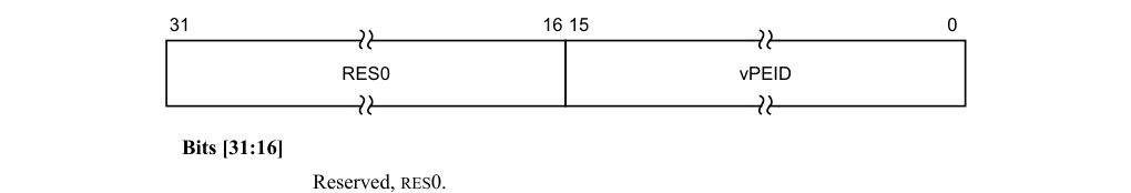
31 16 15 0
RES0 vPEID
Bits [31:16]
Reserved, RES0.
vPEID, bits [15:0]
ID of target vPE
Writing this field is CONSTRAINED UNPREDICTABLE when GICR_VSGIPENDR.Busy == 1, with either the write ignored or a new query started.
Writing a value greater than the configured vPEID width behaviur is CONSTRAINED
UNPREDICTABLE:
-
GICR_VPENDBASER.vPEID is treated as having an UNKNOWN valid value for all purposes other than a direct read of the register.
-
GICR_VPENDBASER.Valid is treated as being set to 0 for all purposes other than a direct read of the register.
The size of this field is IMPLEMENTATION DEFINED, and is specified by the GICD_TYPER2.VIL and GICD_TYPER2.VID fields. Unimplemented bits are RES0.
Accessing the GICR_VSGIR:
64-bit access only.
GICR_VSGIR can be accessed through its memory-mapped interface:
| Component | Frame | Offset | Instance |
|---|---|---|---|
| GIC Redistributor | VLPI_base | 0x0080 | GICR_VSGIR |
This interface is accessible as follows:
-
When GICD_CTLR.DS == 0 accesses to this register are WO.
-
When an access is Secure accesses to this register are WO.
-
When an access is Non-secure accesses to this register are WO.
12.11.40 GICR_WAKER, Redistributor Wake Register
The GICR_WAKER characteristics are:
Purpose
Permits software to control the behavior of the WakeRequest power management signal corresponding to the Redistributor. Power management operations follow the rules in Power management.
Configurations
A copy of this register is provided for each Redistributor.
Attributes
GICR_WAKER is a 32-bit register.
Field descriptions
The GICR_WAKER bit assignments are:
IMP DEF
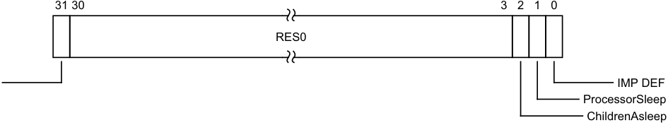
Image text
31 30 3 2 1 0
RES0
IMP DEF
ProcessorSleep
ChildrenAsleep
Bits [30:3]
Reserved, RES0.
ChildrenAsleep, bit [2]
Read-only. Indicates whether the connected PE is quiescent:
0b0 An interface to the connected PE might be active.
0b1 All interfaces to the connected PE are quiescent.
On a Warm reset, this field resets to 1.
ProcessorSleep, bit [1]
Indicates whether the Redistributor can assert the WakeRequest signal:
-
0b0 This PE is not in, and is not entering, a low power state.
-
0b1 The PE is either in, or is in the process of entering, a low power state. All interrupts that arrive at the Redistributor:
-
Assert a WakeRequest signal.
-
Are held in the pending state at the Redistributor, and are not communicated to the CPU interface.
-
Note When ProcessorSleep == 1, the Redistributor must ensure that any interrupts that are pending on the CPU interface are released. For an implementation that is using the GIC Stream Protocol Interface:
-
A Quiesce command puts the interface between the Redistributor and the CPU interface in a quiescent state. For more information, see _Quiesce (IRI)_A-884.
-
A Release command releases any interrupts that are pending on the CPU interface. For more information, see _Release (ICC)_A-885.
Note Before powering down a PE, software must set this bit to 1 and wait until ChildrenAsleep == 1. After powering up a PE, or following a failed powerdown, software must set this bit to 0 and wait until ChildrenAsleep == 0.
Changing ProcessorSleep from 1 to 0 when ChildrenAsleep is not 1 results in UNPREDICTABLE behavior.
Changing ProcessorSleep from 0 to 1 when the Enable for each interrupt group in the associated CPU interface is not 0 results in UNPREDICTABLE behavior.
On a Warm reset, this field resets to 1.
IMPLEMENTATION DEFINED, bit [0]
IMPLEMENTATION DEFINED.
Accessing the GICR_WAKER:
When GICD_CTLR.DS==1, this register is always accessible.
When GICD_CTLR.DS==0, this is a Secure register. This register is RAZ/WI to Non-secure accesses.
To ensure a Redistributor is quiescent, software must write to GICR_WAKER with ProcessorSleep == 1, then poll the register until ChildrenAsleep == 1.
Resetting the connected PE when GICR_WAKER.ProcessorSleep==0 or GICR_WAKER.ChildresAsleep==0, can lead to UNPREDICTABLE behaviour in the IRI.
Resetting the IRI when GICR_WAKER.ProcessorSleep==0 or GICR_WAKER.ChildresAsleep==0 can lead to UNPREDICTABLE behaviour in the connected PE.
GICR_WAKER can be accessed through its memory-mapped interface:
Component Frame Offset Instance GIC Redistributor RD_base 0x0014 GICR_WAKER
This interface is accessible as follows:
-
When GICD_CTLR.DS == 0 accesses to this register are RW.
-
When an access is Secure accesses to this register are RW.
12.12 The GIC CPU interface register map
Table 12-30 shows the CPU interface register maps. In this table, address offsets are relative to the CPU interface base address defined by the system memory map. Unless otherwise stated in the register description, all GIC registers are 32-bits wide.
For a multiprocessor implementation, the GIC implements a set of CPU interface registers for each CPU interface. Arm strongly recommends that each PE has the same CPU interface base address for the CPU interface that connects it to the GIC. This is the private CPU interface base address for that PE. It is IMPLEMENTATION DEFINED whether a PE can access the CPU interface registers of other PEs in the system.
Reserved register addresses are RES0.
The CPU interface registers can be accessed using the System register interface. See GIC System register access for more information.
Table 12-30 CPU interface register map
| Offset | Name | Type | Reset | Description |
|---|---|---|---|---|
| 0x0000 | GICC_CTLR | RW | See the register description | CPU Interface Control Register |
| 0x0004 | GICC_PMR | RW | 0x0000 0000 | Interrupt Priority Mask Register |
| 0x0008 | GICC_BPR | RW | 0x0000 000xa | Binary Point Register |
| 0x000C | GICC_IAR | RO | - | Interrupt Acknowledge Register |
| 0x0010 | GICC_EOIR | WO | - | End of Interrupt Register |
| 0x0014 | GICC_RPR | RO | - | Running Priority Register |
| 0x0018 | GICC_HPPIR | RO | - | Highest Priority Pending Interrupt Register |
| 0x001C | GICC_ABPR | RW | 0x0000 000xa | Aliased Binary Point Register |
| 0x0020 | GICC_AIAR | RO | - | Aliased Interrupt Acknowledge Register |
| 0x0024 | GICC_AEOIR | WO | - | Aliased End of Interrupt Register |
| 0x0028 | GICC_AHPPIR | RO | - | Aliased Highest Priority Pending Interrupt Register |
| 0x002C | GICC_STATUSR | RW | 0x0000 0000 | Error Reporting Status Register, optional |
| 0x0030-0x003C | - | - | - | Reserved |
| 0x0040-0x00CC | - | - | - | IMPLEMENTATION DEFINEDregisters |
| 0x00D0-0x00DC | GICC_APR | RW | 0x0000 0000 | Active Priorities Registers |
| 0x00E0-0x00EC | GICC_NSAPR | RW | 0x0000 0000 | Non-secure Active Priorities Registers |
| 0x00F0-0x00F8 | - | - | - | Reserved |
| 0x00FC | GICC_IIDR | RO | IMPLEMENTATION DEFINED | CPU Interface Identification Register |
| 0x1000 | GICC_DIR | WO | - | Deactivate Interrupt Register |
a. See the register description for more information.
12.13 The GIC CPU interface register descriptions
This section describes each of the GIC CPU interface registers in register name order.
12.13.1 GICC_ABPR, CPU Interface Aliased Binary Point Register
The GICC_ABPR characteristics are:
Purpose
Defines the point at which the priority value fields split into two parts, the group priority field and the subpriority field. The group priority field determines Group 1 interrupt preemption.
Configurations
In systems that support two Security states:
-
This register is an alias of the Non-secure copy of GICC_BPR.
-
Non-secure accesses to this register return a shifted value of the binary point.
-
If ICC_CTLR_EL3.CBPR_EL1NS == 1, Secure accesses to this register access ICC_BPR0_EL1.
Attributes
GICC_ABPR is a 32-bit register.
Field descriptions
The GICC_ABPR bit assignments are:

31 3 2 0
RES0
Binary_Point
Bits [31:3]
Reserved, RES0.
Binary_Point, bits [2:0]
Controls how the 8-bit interrupt priority field is split into a group priority field, that determines interrupt preemption, and a subpriority field. The following list describes how this field determines the interrupt priority bits assigned to the group priority field:
-
Table 4-8, for the processing of Group 1 interrupts in a GIC implementation that supports interrupt grouping, when GICC_CTLR.CBPR == 0.
-
Table 4-9, for all other cases.
On a Warm reset, this field resets to an architecturally UNKNOWN value.
Accessing the GICC_ABPR:
This register is used only when System register access is not enabled. When System register access is enabled, the System registers ICC_BPR0_EL1 and ICC_BPR1_EL1 provide equivalent functionality.
GICC_ABPR can be accessed through its memory-mapped interface:
| Component | Offset | Instance |
|---|---|---|
| GIC CPU interface | 0x001C | GICC_ABPR |
This interface is accessible as follows:
-
When GICD_CTLR.DS == 0 accesses to this register are RW.
-
When an access is Secure accesses to this register are RW.
-
When an access is Non-secure accesses to this register are RW.
12.13.2 GICC_AEOIR, CPU Interface Aliased End Of Interrupt Register
The GICC_AEOIR characteristics are:
Purpose
A write to this register performs priority drop for the specified Group 1 interrupt and, if the appropriate GICC_CTLR.EOImodeS or GICC_CTLR.EOImodeNS field == 0, also deactivates the interrupt.
Configurations
When GICD_CTLR.DS==0, this register is an alias of the Non-secure view of GICC_EOIR. A Secure access to this register is identical to a Non-secure access to GICC_EOIR.
Attributes
GICC_AEOIR is a 32-bit register.
Field descriptions
The GICC_AEOIR bit assignments are:
| | 31 | | 24 | 23 | | 0 | | |—|—|—|—|—|—|—| |||||||||
Bits [31:24]
Reserved, RES0.
INTID, bits [23:0]
The INTID of the signaled interrupt.
Note
INTIDs 1020-1023 are reserved and convey additional information such as spurious interrupts.
When affinity routing is not enabled:
-
Bits [23:13] are RES0.
-
For SGIs, bits [12:10] identify the CPU interface corresponding to the source PE. For all other interrupts these bits are RES0.
Accessing the GICC_AEOIR:
A write to this register must correspond to the most recently acknowledged Group 1 interrupt. If a value other than the last value read from GICC_AIAR is written to this register, the effect is UNPREDICTABLE.
This register is used only when System register access is not enabled. When System register access is enabled:
-
For AArch32 implementations, ICC_EOIR1 provides equivalent functionality.
-
For AArch64 implementations, ICC_EOIR1_EL1 provides equivalent functionality.
When affinity routing is enabled for a Security state, it is a programming error to use memory-mapped registers to access the GIC. GICC_AEOIR can be accessed through its memory-mapped interface:
| Component | Offset | Instance |
|---|---|---|
| GIC CPU interface | 0x0024 | GICC_AEOIR |
This interface is accessible as follows:
-
When GICD_CTLR.DS == 0 accesses to this register are WO.
-
When an access is Secure accesses to this register are WO.
-
When an access is Non-secure accesses to this register are WO.
12.13.3 GICC_AHPPIR, CPU Interface Aliased Highest Priority Pending Interrupt Register
The GICC_AHPPIR characteristics are:
Purpose
If the highest priority pending interrupt is in Group 1, this register provides the INTID of the highest priority pending interrupt on the CPU interface.
Configurations
If GICD_CTLR.DS==0, this register is an alias of the Non-secure view of GICC_HPPIR. A Secure access to this register is identical to a Non-secure access to GICC_HPPIR.
Attributes
GICC_AHPPIR is a 32-bit register.
Field descriptions
The GICC_AHPPIR bit assignments are:
| | 31 | | 24 | 23 | | 0 | | |—|—|—|—|—|—|—| |||||||||
Bits [31:24]
Reserved, RES0.
INTID, bits [23:0]
The INTID of the signaled interrupt.
Note INTIDs 1020-1023 are reserved and convey additional information such as spurious interrupts.
When affinity routing is not enabled:
-
Bits [23:13] are RES0.
-
For SGIs, bits [12:10] identify the CPU interface corresponding to the source PE. For all other interrupts these bits are RES0.
Accessing the GICC_AHPPIR:
This register is used only when System register access is not enabled. When System register access is enabled:
-
For AArch32 implementations, ICC_HPPIR1 provides equivalent functionality.
-
For AArch64 implementations, ICC_HPPIR1_EL1 provides equivalent functionality.
If the highest priority pending interrupt is in Group 0, a read of this register returns the special INTID 1023.
Interrupt identifiers corresponding to an interrupt group that is not enabled are ignored.
If the highest priority pending interrupt is a direct interrupt that is both individually enabled in the Distributor and part of an interrupt group that is enabled in the Distributor, and the interrupt group is disabled in the CPU interface for this PE, this register returns the special INTID 1023.
For more information about pending interrupts that are not considered when determining the highest priority pending interrupt, see Preemption.
When affinity routing is enabled for a Security state, it is a programming error to use memory-mapped registers to access the GIC. GICC_AHPPIR can be accessed through its memory-mapped interface:
| Component | Offset | Instance |
|---|---|---|
| GIC CPU interface | 0x0028 | GICC_AHPPIR |
This interface is accessible as follows:
-
When GICD_CTLR.DS == 0 accesses to this register are RO.
-
When an access is Secure accesses to this register are RO.
-
When an access is Non-secure accesses to this register are RO.
12.13.4 GICC_AIAR, CPU Interface Aliased Interrupt Acknowledge Register
The GICC_AIAR characteristics are:
Purpose
Provides the INTID of the signaled Group 1 interrupt. A read of this register by the PE acts as an acknowledge for the interrupt.
Configurations
When GICD_CTLR.DS==0, this register is an alias of the Non-secure view of GICC_IAR. A Secure access to this register is identical to a Non-secure access to GICC_IAR.
Attributes
GICC_AIAR is a 32-bit register.
Field descriptions
The GICC_AIAR bit assignments are:
| | 31 | | 24 | 23 | | 0 | | |—|—|—|—|—|—|—| |||||||||
Bits [31:24]
Reserved, RES0.
INTID, bits [23:0]
The INTID of the signaled interrupt.
Note INTIDs 1020-1023 are reserved and convey additional information such as spurious interrupts.
When affinity routing is not enabled:
-
Bits [23:13] are RES0.
-
For SGIs, bits [12:10] identify the CPU interface corresponding to the source PE. For all other interrupts these bits are RES0.
Accessing the GICC_AIAR:
When affinity routing is enabled for a Security state, it is a programming error to use memory-mapped registers to access the GIC.
GICC_AIAR can be accessed through its memory-mapped interface:
| Component | Offset | Instance |
|---|---|---|
| GIC CPU interface | 0x0020 | GICC_AIAR |
This interface is accessible as follows:
-
When GICD_CTLR.DS == 0 accesses to this register are RO.
-
When an access is Secure accesses to this register are RO.
-
When an access is Non-secure accesses to this register are RO.
12.13.5 GICC_APR, CPU Interface Active Priorities Registers, n = 0 - 3
The GICC_APR
Purpose
Provides information about interrupt active priorities.
Configurations
The contents of these registers are IMPLEMENTATION DEFINED with the one architectural requirement that the value 0x00000000 is consistent with no interrupts being active.
When GICD_CTLR.DS == 0, these registers are Banked, and Non-secure accesses do not affect Secure operation. The Secure copies of these registers hold active priorities for Group 0 interrupts, and the Non-secure copies provide a Non-secure view of the active priorities for Group 1 interrupts.
GICC_APR1 is only implemented in implementations that support 6 or more bits of priority. GICC_APR2 and GICC_APR3 are only implemented in implementations that support 7 bits of priority.
When GICD_CTLR.DS==1, these registers hold the active priorities for Group 0 interrupts, and the active priorities for Group 1 interrupts are held by the GICC_NSAPR
Attributes
GICC_APR
Field descriptions
The GICC_APR
31 0 IMPLEMENTATION DEFINED
IMPLEMENTATION DEFINED, bits [31:0]
IMPLEMENTATION DEFINED.
On a Warm reset, this field resets to 0.
Accessing the GICC_APR:
These registers are used only when System register access is not enabled. When System register access is enabled the following registers provide equivalent functionality:
-
In AArch64:
-
For Group 0, ICC_AP0R
_EL1. -
For Group 1, ICC_AP1R
_EL1.
-
-
In AArch32:
-
For Group 0, ICC_AP0R
. -
For Group 1, ICC_AP1R
.
-
GICC_APR
| Component | Offset | Instance |
|---|---|---|
| GIC CPU interface | 0x00D0+ (4 * n) | GICC_APR |
| This interface is accessible as follows: |
-
When GICD_CTLR.DS == 0 accesses to this register are RW.
-
When an access is Secure accesses to this register are RW.
-
When an access is Non-secure accesses to this register are RW.
12.13.6 GICC_BPR, CPU Interface Binary Point Register
The GICC_BPR characteristics are:
Purpose
Defines the point at which the priority value fields split into two parts, the group priority field and the subpriority field.
Configurations
In systems that support two Security states:
-
This register is Banked.
-
The Secure instance of this register determines Group 0 interrupt preemption.
-
The Non-secure instance of this register determines Group 1 interrupt preemption.
In systems that support only one Security state, when GICC_CTLR.CBPR == 0, this register determines only Group 0 interrupt preemption.
When GICC_CTLR.CBPR == 1, this register determines interrupt preemption for both Group 0 and Group 1 interrupts.
Attributes
GICC_BPR is a 32-bit register.
Field descriptions
The GICC_BPR bit assignments are:

31 3 2 0
RES0
Binary_Point
Bits [31:3]
Reserved, RES0.
Binary_Point, bits [2:0]
Controls how the 8-bit interrupt priority field is split into a group priority field, that determines interrupt preemption, and a subpriority field. The following list describes how this field determines the interrupt priority bits assigned to the group priority field:
-
Table 4-8, for the processing of Group 1 interrupts in a GIC implementation that supports interrupt grouping, when GICC_CTLR.CBPR == 0.
-
Table 4-9, for all other cases.
On a Warm reset, this field resets to an architecturally UNKNOWN value.
Note Aliasing the Non-secure GICC_BPR as GICC_ABPR in a multiprocessor system permits a PE that can make only Secure accesses to configure the preemption setting for Group 1 interrupts by accessing GICC_ABPR.
Accessing the GICC_BPR:
This register is used only when System register access is not enabled. When System register access is enabled this register is RAZ/WI, and the System registers ICC_BPR0_EL1 and ICC_BPR1_EL1 provide equivalent functionality. GICC_BPR can be accessed through its memory-mapped interface:
| Component | Offset | Instance |
|---|---|---|
| GIC CPU interface | 0x0008 | GICC_BPR |
This interface is accessible as follows:
-
When GICD_CTLR.DS == 0 accesses to this register are RW.
-
When an access is Secure accesses to this register are RW.
-
When an access is Non-secure accesses to this register are RW.
12.13.7 GICC_CTLR, CPU Interface Control Register
The GICC_CTLR characteristics are:
Purpose
Controls the CPU interface, including enabling of interrupt groups, interrupt signal bypass, binary point registers used, and separation of priority drop and interrupt deactivation.
Note
If the GIC implementation supports two Security states, independent EOI controls are provided for accesses from each Security state. Secure accesses handle both Group 0 and Group 1 interrupts, and Non-secure accesses handle Group 1 interrupts only.
Configurations
In a GIC implementation that supports two Security states:
-
This register is Banked.
-
The register bit assignments are different in the Secure and Non-secure copies.
Attributes
GICC_CTLR is a 32-bit register.
Field descriptions
The GICC_CTLR bit assignments are:
When GICD_CTLR.DS==0, Non-secure access:
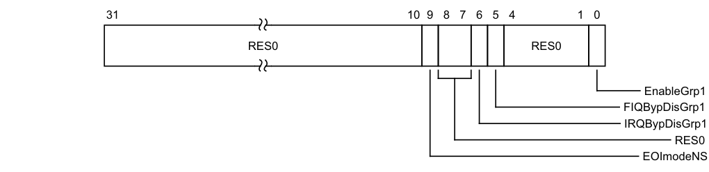
Image text
31 10 9 8 7 6 5 4 1 0
RES0 RES0
EnableGrp1
FIQBypDisGrp1
IRQBypDisGrp1
RES0
EOImodeNS
EOImodeNS, bit [9]
Controls the behavior of Non-secure accesses to GICC_EOIR, GICC_AEOIR, and GICC_DIR.
0b0 GICC_EOIR and GICC_AEOIR provide both priority drop and interrupt deactivation functionality. Accesses to GICC_DIR are UNPREDICTABLE.
- 0b1 GICC_EOIR and GICC_AEOIR provide priority drop functionality only. GICC_DIR provides interrupt deactivation functionality.
Note An implementation is permitted to make this bit RAO/WI.
On a Warm reset, this field resets to 0.
Bits [8:7]
Reserved, RES0.
IRQBypDisGrp1, bit [6]
When the signaling of IRQs by the CPU interface is disabled, this field partly controls whether the bypass IRQ signal is signaled to the PE for Group 1:
0b0 The bypass IRQ signal is signaled to the PE. 0b1 The bypass IRQ signal is not signaled to the PE.
If System register access is enabled for EL3 and ICC_SRE_EL3.DIB == 1, this field is RAO/WI.
If System register access is enabled for EL1, this field is ignored.
If an implementation does not support legacy interrupts, this bit is permitted to be RAO/WI. For more information, see Interrupt bypass support.
On a Warm reset, this field resets to 0.
FIQBypDisGrp1, bit [5]
When the signaling of FIQs by the CPU interface is disabled, this field partly controls whether the bypass FIQ signal is signaled to the PE for Group 1:
0b0 The bypass FIQ signal is signaled to the PE. 0b1 The bypass FIQ signal is not signaled to the PE.
If System register access is enabled for EL3 and ICC_SRE_EL3.DFB == 1, this field is RAO/WI. If System register access is enabled for EL1, this field is ignored.
If an implementation does not support legacy interrupts, this bit is permitted to be RAO/WI. For more information, see Interrupt bypass support.
On a Warm reset, this field resets to 0.
Bits [4:1]
Reserved, RES0.
EnableGrp1, bit [0]
This Non-secure field enables the signaling of Group 1 interrupts by the CPU interface to a target PE:
0b0 Group 1 interrupt signaling is disabled.
0b1 Group 1 interrupt signaling is enabled.
On a Warm reset, this field resets to 0.
When GICD_CTLR.DS==0, Secure access:
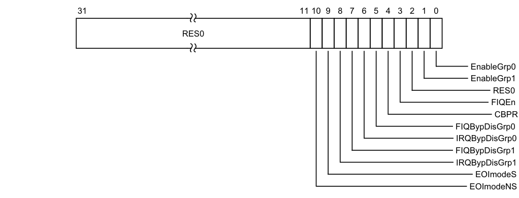
Image text
31 11 10 9 8 7 6 5 4 3 2 1 0
RES0
EnableGrp0
EnableGrp1
RES0
FIQEn
CBPR
FIQBypDisGrp0
IRQBypDisGrp0
FIQBypDisGrp1
IRQBypDisGrp1
EOImodeS
EOImodeNS## Bits [31:11]
Reserved, RES0.
EOImodeNS, bit [10]
Controls the behavior of Non-secure accesses to GICC_EOIR, GICC_AEOIR, and GICC_DIR.
0b0 GICC_EOIR and GICC_AEOIR provide both priority drop and interrupt deactivation functionality. Accesses to GICC_DIR are UNPREDICTABLE.
0b1 GICC_EOIR and GICC_AEOIR provide priority drop functionality only. GICC_DIR provides interrupt deactivation functionality.
Note An implementation is permitted to make this bit RAO/WI.
On a Warm reset, this field resets to 0.
EOImodeS, bit [9]
Controls the behavior of Secure accesses to GICC_EOIR, GICC_AEOIR, and GICC_DIR.
0b0 GICC_EOIR and GICC_AEOIR provide both priority drop and interrupt deactivation functionality. Accesses to GICC_DIR are UNPREDICTABLE.
0b1 GICC_EOIR and GICC_AEOIR provide priority drop functionality only. GICC_DIR provides interrupt deactivation functionality.
Note An implementation is permitted to make this bit RAO/WI.
This field shares state with GICC_CTLR.EOImode.
On a Warm reset, this field resets to 0.
IRQBypDisGrp1, bit [8]
When the signaling of IRQs by the CPU interface is disabled, this field partly controls whether the bypass IRQ signal is signaled to the PE for Group 1:
0b0 The bypass IRQ signal is signaled to the PE. 0b1 The bypass IRQ signal is not signaled to the PE. If System register access is enabled for EL3 and ICC_SRE_EL3ICC_SRE_EL3.DIB == 1, this field is RAO/WI. If System register access is enabled for EL1, this field is ignored.
If System register access is enabled for EL3 and ICC_SRE_EL3ICC_SRE_EL3.DIB == 1, this field is RAO/WI.
If an implementation does not support legacy interrupts, this bit is permitted to be RAO/WI. For more information, see Interrupt bypass support.
On a Warm reset, this field resets to 0.
FIQBypDisGrp1, bit [7]
When the signaling of FIQs by the CPU interface is disabled, this field partly controls whether the bypass FIQ signal is signaled to the PE for Group 1:
0b0 The bypass FIQ signal is signaled to the PE.
0b1 The bypass FIQ signal is not signaled to the PE.
If System register access is enabled for EL3 and ICC_SRE_EL3.DFB == 1, this field is RAO/WI. If System register access is enabled for EL1, this field is ignored.
If an implementation does not support legacy interrupts, this bit is permitted to be RAO/WI. For more information, see Interrupt bypass support.
On a Warm reset, this field resets to 0.
IRQBypDisGrp0, bit [6]
When the signaling of IRQs by the CPU interface is disabled, this field partly controls whether the bypass IRQ signal is signaled to the PE for Group 0:
0b0 The bypass IRQ signal is signaled to the PE. 0b1 The bypass IRQ signal is not signaled to the PE.
If System register access is enabled for EL3 and ICC_SRE_EL3.DIB == 1, this field is RAO/WI. If System register access is enabled for EL1, this field is ignored.
If an implementation does not support legacy interrupts, this bit is permitted to be RAO/WI. For more information, see Interrupt bypass support.
On a Warm reset, this field resets to 0.
FIQBypDisGrp0, bit [5]
When the signaling of FIQs by the CPU interface is disabled, this field partly controls whether the bypass FIQ signal is signaled to the PE for Group 0:
0b0 The bypass FIQ signal is signaled to the PE. 0b1 The bypass FIQ signal is not signaled to the PE.
If System register access is enabled for EL3 and ICC_SRE_EL3.DIB == 1, this field is RAO/WI. If System register access is enabled for EL1, this field is ignored.
If an implementation does not support legacy interrupts, this bit is permitted to be RAO/WI. For more information, see Interrupt bypass support.
On a Warm reset, this field resets to 0.
CBPR, bit [4]
Controls whether GICC_BPR provides common control of preemption to Group 0 and Group 1 interrupts:
0b0 GICC_BPR determines preemption for Group 0 interrupts only. GICC_ABPR determines preemption for Group 1 interrupts.
0b1 GICC_BPR determines preemption for both Group 0 and Group 1 interrupts.
This field is an alias of ICC_CTLR_EL3.CBPR_EL1NS.
In a GIC that supports two Security states, when CBPR == 1:
• A Non-secure read of GICC_BPR returns the value of Secure GICC_BPR.Binary_Point, incremented by 1, and saturated to 0b111.
- Non-secure writes of GICC_BPR are ignored.
On a Warm reset, this field resets to 0.
FIQEn, bit [3]
Controls whether the CPU interface signals Group 0 interrupts to a target PE using the FIQ or IRQ signal:
0b0 Group 0 interrupts are signaled using the IRQ signal.
0b1 Group 0 interrupts are signaled using the FIQ signal.
Group 1 interrupts are signaled using the IRQ signal only.
If an implementation supports two Security states, this bit is permitted to be RAO/WI. On a Warm reset, this field resets to 0.
Bit [2]
Reserved, RES0.
EnableGrp1, bit [1]
This Non-secure field enables the signaling of Group 1 interrupts by the CPU interface to a target PE:
0b0 Group 1 interrupt signaling is disabled. 0b1 Group 1 interrupt signaling is enabled. On a Warm reset, this field resets to 0.
EnableGrp0, bit [0]
Enables the signaling of Group 0 interrupts by the CPU interface to a target PE:
0b0 Group 0 interrupt signaling is disabled. 0b1 Group 0 interrupt signaling is enabled. On a Warm reset, this field resets to 0.
When GICD_CTLR.DS == 1:
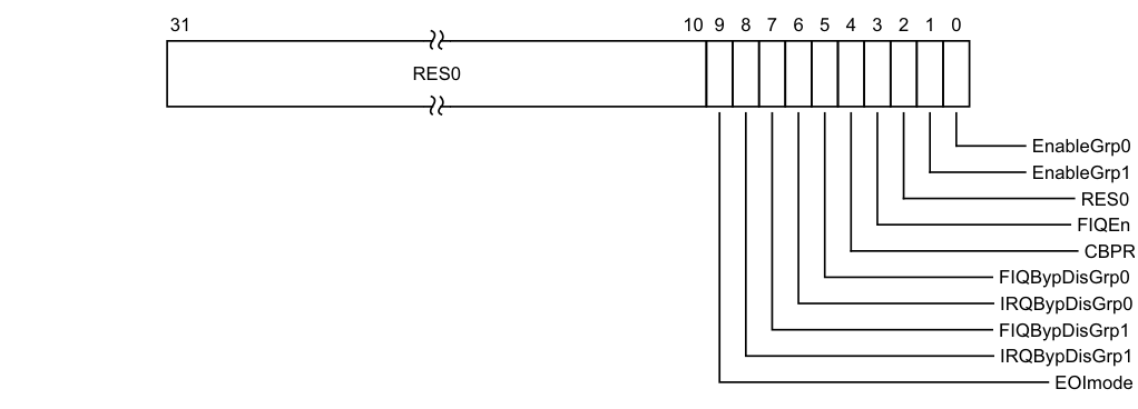
Image text
31 10 9 8 7 6 5 4 3 2 1 0
RES0
EnableGrp0
EnableGrp1
RES0
FIQEn
CBPR
FIQBypDisGrp0
IRQBypDisGrp0
FIQBypDisGrp1
IRQBypDisGrp1
EOImode
Reserved, RES0.
EOImode, bit [9]
Controls the behavior of accesses to GICC_EOIR, GICC_AEOIR, and GICC_DIR.
0b0 GICC_EOIR and GICC_AEOIR provide both priority drop and interrupt deactivation functionality. Accesses to GICC_DIR are UNPREDICTABLE. 0b1 GICC_EOIR and GICC_AEOIR provide priority drop functionality only. GICC_DIR provides interrupt deactivation functionality.
Note An implementation is permitted to make this bit RAO/WI.
This field shares state with GICC_CTLR.EOImodeS.
On a Warm reset, this field resets to 0.
IRQBypDisGrp1, bit [8]
When the signaling of IRQs by the CPU interface is disabled, this field partly controls whether the bypass IRQ signal is signaled to the PE for Group 1:
0b0 The bypass IRQ signal is signaled to the PE. 0b1 The bypass IRQ signal is not signaled to the PE. If System register access is enabled for EL3 and ICC_SRE_EL3.DIB == 1, this field is RAO/WI. If System register access is enabled for EL1, this field is ignored.
If an implementation does not support legacy interrupts, this bit is permitted to be RAO/WI. For more information, see Interrupt bypass support.
On a Warm reset, this field resets to 0.
FIQBypDisGrp1, bit [7]
When the signaling of FIQs by the CPU interface is disabled, this field partly controls whether the bypass FIQ signal is signaled to the PE for Group 1:
0b0 The bypass FIQ signal is signaled to the PE. 0b1 The bypass FIQ signal is not signaled to the PE.
If System register access is enabled for EL3 and ICC_SRE_EL3.DFB == 1, this field is RAO/WI. If System register access is enabled for EL1, this field is ignored.
If an implementation does not support legacy interrupts, this bit is permitted to be RAO/WI. For more information, see Interrupt bypass support.
On a Warm reset, this field resets to 0.
IRQBypDisGrp0, bit [6]
When the signaling of IRQs by the CPU interface is disabled, this field partly controls whether the bypass IRQ signal is signaled to the PE for Group 0:
0b0 The bypass IRQ signal is signaled to the PE. 0b1 The bypass IRQ signal is not signaled to the PE.
If System register access is enabled for EL3 and ICC_SRE_EL3.DIB == 1, this field is RAO/WI. If System register access is enabled for EL1, this field is ignored.
If an implementation does not support legacy interrupts, this bit is permitted to be RAO/WI. For more information, see Interrupt bypass support.
On a Warm reset, this field resets to 0.
FIQBypDisGrp0, bit [5]
When the signaling of FIQs by the CPU interface is disabled, this field partly controls whether the bypass FIQ signal is signaled to the PE for Group 0:
0b0 The bypass FIQ signal is signaled to the PE. 0b1 The bypass FIQ signal is not signaled to the PE.
If System register access is enabled for EL3 and ICC_SRE_EL3.DIB == 1, this field is RAO/WI. If System register access is enabled for EL1, this field is ignored. If an implementation does not support legacy interrupts, this bit is permitted to be RAO/WI. For more information, see Interrupt bypass support. On a Warm reset, this field resets to 0.
CBPR, bit [4]
Controls whether GICC_BPR provides common control of preemption to Group 0 and Group 1 interrupts:
0b0 GICC_BPR determines preemption for Group 0 interrupts only. GICC_ABPR determines preemption for Group 1 interrupts. 0b1 GICC_BPR determines preemption for both Group 0 and Group 1 interrupts. This field is an alias of ICC_CTLR_EL3.CBPR_EL1NS. In a GIC that supports two Security states, when CBPR == 1:
-
A Non-secure read of GICC_BPR returns the value of Secure GICC_BPR.Binary_Point, incremented by 1, and saturated to 0b111.
-
Non-secure writes of GICC_BPR are ignored.
On a Warm reset, this field resets to 0.
FIQEn, bit [3]
Controls whether the CPU interface signals Group 0 interrupts to a target PE using the FIQ or IRQ signal:
0b0 Group 0 interrupts are signaled using the IRQ signal.
0b1 Group 0 interrupts are signaled using the FIQ signal.
Group 1 interrupts are signaled using the IRQ signal only.
If an implementation supports two Security states, this bit is permitted to be RAO/WI.
On a Warm reset, this field resets to 0.
Bit [2]
Reserved, RES0.
EnableGrp1, bit [1]
This Non-secure field enables the signaling of Group 1 interrupts by the CPU interface to a target PE:
0b0 Group 1 interrupt signaling is disabled. 0b1 Group 1 interrupt signaling is enabled.
On a Warm reset, this field resets to 0.
EnableGrp0, bit [0]
Enables the signaling of Group 0 interrupts by the CPU interface to a target PE:
0b0 Group 0 interrupt signaling is disabled. 0b1 Group 0 interrupt signaling is enabled. On a Warm reset, this field resets to 0.
Accessing the GICC_CTLR:
This register is used only when System register access is not enabled. When System register access is enabled:
-
For AArch32 implementations, ICC_CTLR and ICC_MCTLR provide equivalent functionality.
-
For AArch64 implementations, ICC_CTLR_EL1 and ICC_CTLR_EL3 provide equivalent functionality.
GICC_CTLR can be accessed through its memory-mapped interface:
Component Offset Instance GIC CPU interface 0x0000 GICC_CTLR
This interface is accessible as follows:
-
When GICD_CTLR.DS == 0 accesses to this register are RW.
-
When an access is Secure accesses to this register are RW.
-
When an access is Non-secure accesses to this register are RW.
12.13.8 GICC_DIR, CPU Interface Deactivate Interrupt Register
The GICC_DIR characteristics are:
Purpose
When interrupt priority drop is separated from interrupt deactivation, a write to this register deactivates the specified interrupt.
Configurations
There are no configuration notes.
Attributes
GICC_DIR is a 32-bit register.
Field descriptions
The GICC_DIR bit assignments are:
| | 31 | | 24 | 23 | | 0 | | |—|—|—|—|—|—|—| |||||||||
Bits [31:24]
Reserved, RES0.
INTID, bits [23:0]
The INTID of the signaled interrupt.
Note INTIDs 1020-1023 are reserved and convey additional information such as spurious interrupts.
When affinity routing is not enabled:
-
Bits [23:13] are RES0.
-
For SGIs, bits [12:10] identify the CPU interface corresponding to the source PE. For all other interrupts these bits are RES0.
Accessing the GICC_DIR:
This register is used only when System register access is not enabled. When System register access is enabled:
-
For AArch32 implementations, ICC_DIR provides equivalent functionality.
-
For AArch64 implementations, ICC_DIR_EL1 provides equivalent functionality.
Writes to this register have an effect only in the following cases:
-
When GICD_CTLR.DS == 1, if GICC_CTLR.EOImode == 1.
-
In GIC implementations that support two Security states:
-
If the access is Secure and GICC_CTLR.EOImodeS == 1.
-
If the access is Non-secure and GICC_CTLR.EOImodeNS == 1.
-
The following writes must be ignored:
- Writes to this register when the corresponding EOImode field in GICC_CTLR == 0. In systems that support system error generation, an implementation might generate a system error.
- Writes to this register when the corresponding EOImode field in GICC_CTLR == 0 and the corresponding interrupt is not active. In systems that support system error generation, an implementation might generate a system error. In implementations using the GIC Stream Protocol Interface, these writes correspond to a Deactivate packet for an interrupt that is not active. For more information, see _Deactivate (ICC)_A-879.
If the corresponding EOImode field in GICC_CTLR is 1 and this register is written to without a corresponding write to GICC_EOIR or GICC_AEOIR, the interrupt is deactivated but the bit corresponding to it in the active priorities registers remains set.
When affinity routing is enabled for a Security state, it is a programming error to use memory-mapped registers to access the GIC.
GICC_DIR can be accessed through its memory-mapped interface:
Component Offset Instance
GIC CPU interface 0x1000 GICC_DIR
This interface is accessible as follows:
-
When GICD_CTLR.DS == 0 accesses to this register are WO.
-
When an access is Secure accesses to this register are WO.
-
When an access is Non-secure accesses to this register are WO.
12.13.9 GICC_EOIR, CPU Interface End Of Interrupt Register
The GICC_EOIR characteristics are:
Purpose
A write to this register performs priority drop for the specified interrupt and, if the appropriate GICC_CTLR.EOImodeS or GICC_CTLR.EOImodeNS field == 0, also deactivates the interrupt.
Configurations
If GICD_CTLR.DS==0:
-
This register is Common.
-
GICC_AEOIR is an alias of the Non-secure view of this register.
For Secure writes when GICD_CTLR.DS==0, or for Secure and Non-secure writes when GICD_CTLR.DS==1, the register provides functionality for Group 0 interrupts.
For Non-secure writes when GICD_CTLR.DS==1, the register provides functionality for Group 1 interrupts.
Attributes
GICC_EOIR is a 32-bit register.
Field descriptions
The GICC_EOIR bit assignments are:
| | 31 | | 24 | 23 | | 0 | | |—|—|—|—|—|—|—| |||||||||
Bits [31:24]
Reserved, RES0.
INTID, bits [23:0]
The INTID of the signaled interrupt.
Note INTIDs 1020-1023 are reserved and convey additional information such as spurious interrupts.
When affinity routing is not enabled:
-
Bits [23:13] are RES0.
-
For SGIs, bits [12:10] identify the CPU interface corresponding to the source PE. For all other interrupts these bits are RES0.
For every read of a valid INTID from GICC_IAR, the connected PE must perform a matching write to GICC_EOIR. The value written to GICC_EOIR must be the INTID from GICC_IAR. Reads of INTIDs 1020-1023 do not require matching writes.
Note Arm recommends that software preserves the entire register value read from GICC_IAR, and writes that value back to GICC_EOIR on completion of interrupt processing.
For nested interrupts, the order of writes to this register must be the reverse of the order of interrupt acknowledgement. Behavior is UNPREDICTABLE if:
-
This ordering constraint is not maintained.
-
The value written to this register does not match an active interrupt, or the ID of a spurious interrupt.
-
The value written to this register does not match the last valid interrupt value read from GICC_IAR.
For general information about the effect of writes to end of interrupt registers, and about the possible separation of the priority drop and interrupt deactivate operations, see Interrupt lifecycle.
If GICD_CTLR.DS==0:
-
GICC_CTLR.EOImodeS controls the behavior of Secure accesses to GICC_EOIR and GICC_AEOIR.
-
GICC_CTLR.EOImodeNS controls the behavior of Non-secure accesses to GICC_EOIR and GICC_AEOIR.
Accessing the GICC_EOIR:
The following writes must be ignored:
-
Writes of INTIDs 1020-1023.
-
Secure writes corresponding to Group 1 interrupts. In systems that support system error generation, an implementation might generate a system error. In this case, GIC behavior is predictable, and the highest Secure active priority (in the Secure copy of GICC_APR
) will be reset if the highest active priority is Secure. System behavior is UNPREDICTABLE. -
Non-secure writes corresponding to Group 0 interrupts when GICC_CTLR.EOImodeS == 1. In systems that support system error generation, an implementation might generate a system error. In this case, GIC behavior is predictable, and the highest Non-secure active priority (in the Non-secure copy of GICC_APR
) will be reset if the highest active priority is Non-secure. System behavior is UNPREDICTABLE.
This register is used only when System register access is not enabled. When System register access is enabled:
-
For AArch32 implementations, ICC_EOIR0 and ICC_EOIR1 provide equivalent functionality.
-
For AArch64 implementations, ICC_EOIR0_EL1 and ICC_EOIR1_EL1 provide equivalent functionality.
When affinity routing is enabled for a Security state, it is a programming error to use memory-mapped registers to access the GIC.
GICC_EOIR can be accessed through its memory-mapped interface:
Component Offset Instance GIC CPU interface 0x0010 GICC_EOIR
This interface is accessible as follows:
-
When GICD_CTLR.DS == 0 accesses to this register are WO.
-
When an access is Secure accesses to this register are WO.
-
When an access is Non-secure accesses to this register are WO.
12.13.10 GICC_HPPIR, CPU Interface Highest Priority Pending Interrupt Register
The GICC_HPPIR characteristics are:
Purpose
Provides the INTID of the highest priority pending interrupt on the CPU interface.
Configurations
If GICD_CTLR.DS==0:
-
This register is Common.
-
GICC_AHPPIR is an alias of the Non-secure view of this register.
Attributes
GICC_HPPIR is a 32-bit register.
Field descriptions
The GICC_HPPIR bit assignments are:

31 24 23 0
RES0 INTID
Bits [31:24]
Reserved, RES0.
INTID, bits [23:0]
The INTID of the signaled interrupt.
Note INTIDs 1020-1023 are reserved and convey additional information such as spurious interrupts.
When affinity routing is not enabled:
-
Bits [23:13] are RES0.
-
For SGIs, bits [12:10] identify the CPU interface corresponding to the source PE. For all other interrupts these bits are RES0.
Accessing the GICC_HPPIR:
This register is used only when System register access is not enabled. When System register access is enabled:
-
For AArch32 implementations, ICC_HPPIR0 and ICC_HPPIR1 provide equivalent functionality.
-
For AArch64 implementations, ICC_HPPIR0_EL1 and ICC_HPPIR1_EL1 provide equivalent functionality.
If the highest priority pending interrupt is in Group 0, a Non-secure read of this register returns the special INTID 1023.
For Secure reads when GICD_CTLR.DS==0, or for Secure and Non-secure reads when GICD_CTLR.DS==1, returns the special INTID 1022 if the highest priority pending interrupt is in Group 1.
If no interrupts are in the pending state, a read of this register returns the special INTID 1023.
Interrupt identifiers corresponding to an interrupt group that is not enabled are ignored. If the highest priority pending interrupt is a direct interrupt that is both individually enabled in the Distributor and part of an interrupt group that is enabled in the Distributor, and the interrupt group is disabled in the CPU interface for this PE, this register returns the special INTID 1023.
For more information about pending interrupts that are not considered when determining the highest priority pending interrupt, see Preemption.
When affinity routing is enabled for a Security state, it is a programming error to use memory-mapped registers to access the GIC.
GICC_HPPIR can be accessed through its memory-mapped interface:
| Component | Offset | Instance |
|---|---|---|
| GIC CPU interface | 0x0018 | GICC_HPPIR |
This interface is accessible as follows:
-
When GICD_CTLR.DS == 0 accesses to this register are RO.
-
When an access is Secure accesses to this register are RO.
-
When an access is Non-secure accesses to this register are RO.
12.13.11 GICC_IAR, CPU Interface Interrupt Acknowledge Register
The GICC_IAR characteristics are:
Purpose
Provides the INTID of the signaled interrupt. A read of this register by the PE acts as an acknowledge for the interrupt.
Configurations
This register is available in all configurations of the GIC. If GICD_CTLR.DS==0:
-
This register is Common.
-
GICC_AIAR is an alias of the Non-secure view of this register.
The format of the INTID is governed by whether affinity routing is enabled for a Security state.
Attributes
GICC_IAR is a 32-bit register.
Field descriptions
The GICC_IAR bit assignments are:
| | 31 | | 24 | 23 | | 0 | | |—|—|—|—|—|—|—| |||||||||
Bits [31:24]
Reserved, RES0.
INTID, bits [23:0]
The INTID of the signaled interrupt.
Note INTIDs 1020-1023 are reserved and convey additional information such as spurious interrupts.
When affinity routing is not enabled:
-
Bits [23:13] are RES0.
-
For SGIs, bits [12:10] identify the CPU interface corresponding to the source PE. For all other interrupts these bits are RES0.
A read of this register returns the INTID of the highest priority pending interrupt for the CPU interface. The read returns a spurious INTID of 1023 if any of the following apply:
-
Forwarding of interrupts by the Distributor to the CPU interface is disabled.
-
Signaling of interrupts by the CPU interface to the connected PE is disabled.
-
There are no pending interrupts on the CPU interface with sufficient priority for the interface to signal it to the PE.
When the GIC returns a valid INTID to a read of this register it treats the read as an acknowledge of that interrupt. In addition, it changes the interrupt status from pending to active, or to active and pending if the pending state of the interrupt persists. Normally, the pending state of an interrupt persists only if the interrupt is level-sensitive and remains asserted.
For every read of a valid INTID from GICC_IAR, the connected PE must perform a matching write to GICC_EOIR.
Note
-
Arm recommends that software preserves the entire register value read from this register, and writes that value back to GICC_EOIR on completion of interrupt processing.
-
For SPIs, although multiple target PEs might attempt to read this register at any time, only one PE can obtain a valid INTID. For more information, see Activation.
Accessing the GICC_IAR:
When GICD_CTLR.DS==1, if the highest priority pending interrupt is in Group 1, the special INTID 1022 is returned.
In GIC implementations that support two Security states, if the highest priority pending interrupt is in Group 0, Non-secure reads return the special INTID 1023.
In GIC implementations that support two Security states, if the highest priority pending interrupt is in Group 1, Secure reads return the special INTID 1022.
This register is used only when System register access is not enabled. When System register access is enabled:
-
For AArch32 implementations, ICC_IAR0 and ICC_IAR1 provide equivalent functionality.
-
For AArch64 implementations, ICC_IAR0_EL1 and ICC_IAR1_EL1 provide equivalent functionality.
When affinity routing is enabled for a Security state, it is a programming error to use memory-mapped registers to access the GIC.
GICC_IAR can be accessed through its memory-mapped interface:
Component Offset Instance
GIC CPU interface 0x000C GICC_IAR
This interface is accessible as follows:
-
When GICD_CTLR.DS == 0 accesses to this register are RO.
-
When an access is Secure accesses to this register are RO.
-
When an access is Non-secure accesses to this register are RO.
12.13.12 GICC_IIDR, CPU Interface Identification Register
The GICC_IIDR characteristics are:
Purpose
Provides information about the implementer and revision of the CPU interface.
Configurations
There are no configuration notes.
Attributes
GICC_IIDR is a 32-bit register.
Field descriptions
The GICC_IIDR bit assignments are:
| 31 20 19 16 15 12 11 0 | 31 20 19 16 15 12 11 0 | 31 20 19 16 15 12 11 0 | 31 20 19 16 15 12 11 0 | 31 20 19 16 15 12 11 0 |
|---|---|---|---|---|
| ProductID | Revision | Implementer | ||
Architecture_version
ProductID, bits [31:20]
An IMPLEMENTATION DEFINED product identifier.
Architecture_version, bits [19:16]
The version of the GIC architecture that is implemented.
0b0001 GICv1. 0b0010 GICv2. 0b0011 FEAT_GICv3 memory-mapped interface supported. Support for the System register interface is discoverable from PE registers ID_PFR1 and ID_AA64PFR0_EL1. 0b0100 FEAT_GICv4 memory-mapped interface supported. Support for the System register interface is discoverable from PE registers ID_PFR1 and ID_AA64PFR0_EL1.
Other values are reserved.
Revision, bits [15:12]
An IMPLEMENTATION DEFINED revision number for the CPU interface.
Implementer, bits [11:0]
Contains the JEP106 code of the company that implemented the CPU interface.
-
Bits [11:8] are the JEP106 continuation code of the implementer. For an Arm implementation, this field is 0x4.
-
Bit [7] is always 0.
-
Bits [6:0] are the JEP106 identity code of the implementer. For an Arm implementation, bits [7:0] are therefore 0x3B.
Accessing the GICC_IIDR:
GICC_IIDR can be accessed through its memory-mapped interface:
| Component | Offset | Instance |
|---|---|---|
| GIC CPU interface | 0x00FC | GICC_IIDR |
This interface is accessible as follows:
-
When GICD_CTLR.DS == 0 accesses to this register are RO.
-
When an access is Secure accesses to this register are RO.
-
When an access is Non-secure accesses to this register are RO.
12.13.13 GICC_NSAPR, CPU Interface Non-secure Active Priorities Registers, n = 0 - 3
The GICC_NSAPR
Purpose
Provides information about Group 1 interrupt active priorities.
Configurations
The contents of these registers are IMPLEMENTATION DEFINED with the one architectural requirement that the value 0x00000000 is consistent with no interrupts being active.
When GICD_CTLR.DS==0, these registers are RAZ/WI to Non-secure accesses.
GICC_NSAPR1 is only implemented in implementations that support 6 or more bits of priority. GICC_NSAPR2 and GICC_NSAPR3 are only implemented in implementations that support 7 bits of priority.
Attributes
GICC_NSAPR
Field descriptions
The GICC_NSAPR

31 0
IMPLEMENTATION DEFINED
IMPLEMENTATION DEFINED, bits [31:0]
IMPLEMENTATION DEFINED.
On a Warm reset, this field resets to 0.
Accessing the GICC_NSAPR:
GICC_NSAPR
| Component | Offset | Instance |
|---|---|---|
| GIC CPU interface | 0x00E0+ (4 * n) | GICC_NSAPR |
This interface is accessible as follows:
-
When GICD_CTLR.DS == 0 accesses to this register are RW.
-
When an access is Secure accesses to this register are RW.
-
When an access is Non-secure accesses to this register are RW.
12.13.14 GICC_PMR, CPU Interface Priority Mask Register
The GICC_PMR characteristics are:
Purpose
This register provides an interrupt priority filter. Only interrupts with a higher priority than the value in this register are signaled to the PE.
Note Higher interrupt priority corresponds to a lower value of the Priority field.
Configurations
This register is available in all configurations of the GIC. If the GIC implementation supports two Security states this register is Common.
Attributes
GICC_PMR is a 32-bit register.
Field descriptions
The GICC_PMR bit assignments are:

31 8 7 0
RES0 Priority
Bits [31:8]
Reserved, RES0.
Priority, bits [7:0]
The priority mask level for the CPU interface. If the priority of the interrupt is higher than the value indicated by this field, the interface signals the interrupt to the PE.
If the GIC implementation supports fewer than 256 priority levels some bits might be RAZ/WI, as follows:
-
For 128 supported levels, bit [0] = 0b0.
-
For 64 supported levels, bits [1:0] = 0b00.
-
For 32 supported levels, bits [2:0] = 0b000.
-
For 16 supported levels, bits [3:0] = 0b0000.
For more information, see Interrupt prioritization.
On a Warm reset, this field resets to an architecturally UNKNOWN value.
Accessing the GICC_PMR:
If the GIC implementation supports two Security states:
-
Non-secure accesses to this register can only read or write values corresponding to the lower half of the priority range.
-
If a Secure write has programmed the register with a value that corresponds to a value in the upper half of the priority range then:
- Any Non-secure read of the register returns 0x00, regardless of the value held in the register.
-
Non-secure writes are ignored. For more information, see Interrupt prioritization.
GICC_PMR can be accessed through its memory-mapped interface:
| Component | Offset | Instance |
|---|---|---|
| GIC CPU interface | 0x0004 | GICC_PMR |
This interface is accessible as follows:
-
When GICD_CTLR.DS == 0 accesses to this register are RW.
-
When an access is Secure accesses to this register are RW.
-
When an access is Non-secure accesses to this register are RW.
12.13.15 GICC_RPR, CPU Interface Running Priority Register
The GICC_RPR characteristics are:
Purpose
This register indicates the running priority of the CPU interface.
Configurations
This register is available in all configurations of the GIC. If the GIC implementation supports two Security states this register is Common.
Attributes
GICC_RPR is a 32-bit register.
Field descriptions
The GICC_RPR bit assignments are:

31 8 7 0
RES0 Priority
Bits [31:8]
Reserved, RES0.
Priority, bits [7:0]
The current running priority on the CPU interface. This is the group priority of the current active interrupt.
If there are no active interrupts on the CPU interface, or all active interrupts have undergone a priority drop, the value returned is the Idle priority.
The priority returned is the group priority as if the BPR was set to the minimum value.
Accessing the GICC_RPR:
If there is no active interrupt on the CPU interface, the idle priority value is returned.
If the GIC implementation supports two Security states, a Non-secure read of the Priority field returns:
-
0x00 if the field value is less than 0x80.
-
The Non-secure view of the Priority value if the field value is 0x80 or more.
For more information, see Interrupt prioritization.
Note Software cannot determine the number of implemented priority bits from this register.
GICC_RPR can be accessed through its memory-mapped interface:
Component Offset Instance GIC CPU interface 0x0014 GICC_RPR This interface is accessible as follows:
-
When GICD_CTLR.DS == 0 accesses to this register are RO.
-
When an access is Secure accesses to this register are RO.
-
When an access is Non-secure accesses to this register are RO.
12.13.16 GICC_STATUSR, CPU Interface Status Register
The GICC_STATUSR characteristics are:
Purpose
Provides software with a mechanism to detect:
-
Accesses to reserved locations.
-
Writes to read-only locations.
-
Reads of write-only locations.
Configurations
If the GIC implementation supports two Security states this register is Banked to provide Secure and Non-secure copies.
This register is used only when System register access is not enabled. If System register access is enabled, this register is not updated. Equivalent functionality might be provided by appropriate traps and exceptions.
Attributes
GICC_STATUSR is a 32-bit register.
Field descriptions
The GICC_STATUSR bit assignments are:
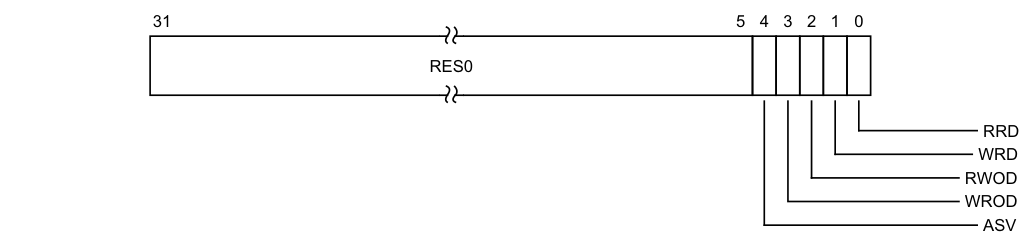
Image text
31 5 4 3 2 1 0
RES0
RRD
WRD
RWOD
WROD
ASV
ASV, bit [4]
Attempted security violation.
0b0 Normal operation. 0b1 A Non-secure access to a Secure register has been detected. Note This bit is not set to 1 for registers where any of the fields are Non-secure.
WROD, bit [3]
Write to an RO location. 0b0 Normal operation. 0b1 A write to an RO location has been detected. When a violation is detected, software must write 1 to this register to reset it.
RWOD, bit [2]
Read of a WO location.
0b0 Normal operation. 0b1 A read of a WO location has been detected.
When a violation is detected, software must write 1 to this register to reset it.
WRD, bit [1]
Write to a reserved location. 0b0 Normal operation. 0b1 A write to a reserved location has been detected. When a violation is detected, software must write 1 to this register to reset it.
RRD, bit [0]
Read of a reserved location. 0b0 Normal operation. 0b1 A read of a reserved location has been detected. When a violation is detected, software must write 1 to this register to reset it.
Accessing the GICC_STATUSR:
This is an optional register. If the register is not implemented, the location is RAZ/WI.
If this register is implemented, GICV_STATUSR must also be implemented.
GICC_STATUSR can be accessed through its memory-mapped interface:
Component Offset Instance GIC CPU interface 0x002C GICC_STATUSR (S)
This interface is accessible as follows:
-
When GICD_CTLR.DS == 0 accesses to this register are RW.
-
When an access is Secure accesses to this register are RW.
GICC_STATUSR can be accessed through its memory-mapped interface:
Component Offset Instance GIC CPU interface 0x002C GICC_STATUSR (NS)
This interface is accessible as follows:
-
When GICD_CTLR.DS == 0 accesses to this register are RW.
-
When an access is Non-secure accesses to this register are RW.
12.14 The GIC virtual CPU interface register map
Note Unless explicitly defined otherwise in this section, the GICV_* registers are as defined in the GICv2 specification, see Arm[®] Generic Interrupt Controller, Architecture version 2.0, Architecture Specification .
These registers provide the virtual CPU interface accessed by the virtual machine. Typically, a virtual machine is unaware of any difference between virtual interrupts and physical interrupts. This means the programmers’ model for handling virtual interrupts must be identical to that for handling physical interrupts. In general, these registers have the same format as the GIC physical CPU interface registers, but they operate on the interrupt view defined primarily by the List registers.
These registers are memory-mapped, with defined offsets from an IMPLEMENTATION DEFINED GICV_* register base address.
Note The offset of each GICV_* register is the same as the offset of the corresponding register for the physical CPU interface. For example, GICV_PMR is at offset 0x0004 from the GICV_* register base address, and GICC_PMR is at the same offset from the GICC_* register base address.
This means that:
-
The hypervisor can use the stage 2 address translations to map the virtual CPU interface accesses to the correct physical addresses.
-
Software, whether accessing the registers of a physical CPU interface or of a virtual CPU interface, uses the same register addresses.
To enable use of 64KB pages, the GICV_* memory map must ensure that:
-
The base address of the GICV_* registers is 64KB aligned.
-
An alias of the GICV_* registers is provided starting at offset 0xF000 from the start of the page such that a second copy of GICV_DIR exists at the start of the next 64KB page.
This provides support for both 4KB and 64KB pages.
Reserved register addresses are RES0.
Table 12-31 shows the GIC virtual CPU interface register map.
Table 12-31 GIC virtual CPU interface register map
| Offset | Name | Type | Reset | Description |
|---|---|---|---|---|
| 0x0000 | GICV_CTLR | RW | See the register description | VM Control Register |
| 0x0004 | GICV_PMR | RW | 0x0000 0000 | VM Priority Mask Register |
| 0x0008 | GICV_BPR | RW | 0x0000 000xa | VM Binary Point Register |
| 0x000C | GICV_IAR | RO | - | VM Interrupt Acknowledge Register |
| 0x0010 | GICV_EOIR | WO | - | VM End of Interrupt Register |
| 0x0014 | GICV_RPR | RO | - | VM Running Priority Register |
| 0x0018 | GICV_HPPIR | RO | - | VM Highest Priority Pending Interrupt Register |
| 0x001C | GICV_ABPR | RW | 0x0000 000xa | VM Aliased Binary Point Register |
| 0x0020 | GICV_AIAR | RO | - | VM Aliased Interrupt Acknowledge Register |
| Table 12-31 GIC virtual CPU interface register map (continued) |
| Offset | Name | Type | Reset | Description |
|---|---|---|---|---|
| 0x0024 | GICV_AEOIR | WO | - | VM Aliased End of Interrupt Register |
| 0x0028 | GICV_AHPPIR | RO | - | VM Aliased Highest Priority Pending Interrupt Register |
| 0x002C | GICV_STATUSR | RW | 0x0000 0000 | VM Error Reporting Status Register, optional |
| 0x0030-0x003C | - | - | - | Reserved |
| 0x0040-0x00CC | - | - | - | IMPLEMENTATION DEFINED |
| 0x00D0-0x00DC | GICV_APR | RW | 0x0000 0000 | VM Active Priorities Registers |
| 0x00E0-0x00EC | - | - | RAZ/WI | Reserved for second set of Active Priorities Registers, as the Note in the description describes |
| 0x00F0-0x00F8 | - | - | - | Reserved |
| 0x00FC | GICV_IIDR | RO | IMPLEMENTATION DEFINED | VM CPU Interface Identification Register |
| 0x0100-0x0FFC | - | - | - | Reserved |
| 0x1000 0x10000 | GICV_DIR | WO | - | VM Deactivate Interrupt Register |
| 0x1004-0x1FFC | - | - | - | Reserved |
a. See the register description for more information.
12.15 The GIC virtual CPU interface register descriptions
This section describes each of the GIC virtual CPU interface registers in register name order.
12.15.1 GICV_ABPR, Virtual Machine Aliased Binary Point Register
The GICV_ABPR characteristics are:
Purpose
Defines the point at which the priority value fields split into two parts, the group priority field and the subpriority field. The group priority field determines Group 1 interrupt preemption. This register corresponds to GICC_ABPR in the physical CPU interface.
Note GICH_LR
.Group determines whether a virtual interrupt is Group 0 or Group 1.
Configurations
This register is available when the GIC implementation supports interrupt virtualization.
Attributes
GICV_ABPR is a 32-bit register.
Field descriptions
The GICV_ABPR bit assignments are:

31 3 2 0
RES0
Binary_Point
Bits [31:3]
Reserved, RES0.
Binary_Point, bits [2:0]
Controls how the 8-bit interrupt priority field is split into a group priority field, that determines interrupt preemption, and a subpriority field.
For information about how this field determines the interrupt priority bits assigned to the group priority field, see Priority grouping.
On a Warm reset, this field resets to 0.
The Binary_Point field of this register is aliased to GICH_VMCR.VBPR1.
Accessing the GICV_ABPR:
This register is used only when System register access is not enabled. When System register access is enabled:
-
For AArch32 implementations, ICC_BPR1 provides equivalent functionality.
-
For AArch64 implementations, ICC_BPR1_EL1 provides equivalent functionality.
The value contained in this register is one greater than the actual applied binary point value, as described in Priority grouping.
This register is used for Group 1 interrupts when GICV_CTLR.CBPR == 0. GICV_BPR provides equivalent functionality for Group 0 interrupts, and for Group 1 interrupts when GICV_CTLR.CBPR == 1. GICV_ABPR can be accessed through its memory-mapped interface:
| Component | Offset | Instance |
|---|---|---|
| GIC Virtual CPU interface | 0x001C | GICV_ABPR |
This interface is accessible as follows:
-
When GICD_CTLR.DS == 0 accesses to this register are RW.
-
When an access is Secure accesses to this register are RW.
-
When an access is Non-secure accesses to this register are RW.
12.15.2 GICV_AEOIR, Virtual Machine Aliased End Of Interrupt Register
The GICV_AEOIR characteristics are:
Purpose
A write to this register performs a priority drop for the specified Group 1 virtual interrupt and, if GICV_CTLR.EOImode == 0, also deactivates the interrupt.
Configurations
This register is available when the GIC implementation supports interrupt virtualization.
Attributes
GICV_AEOIR is a 32-bit register.
Field descriptions
The GICV_AEOIR bit assignments are:
| | 31 | | 25 | 24 | | 0 | | |—|—|—|—|—|—|—| |||||||||
Bits [31:25]
Reserved, RES0.
INTID, bits [24:0]
The INTID of the signaled interrupt.
Note INTIDs 1020-1023 are reserved and convey additional information such as spurious interrupts.
When affinity routing is not enabled:
-
Bits [23:13] are RES0.
-
For SGIs, bits [12:10] identify the CPU interface corresponding to the source PE. For all other interrupts these bits are RES0.
A successful EOI request means that:
-
The highest priority bit in GICH_APR
is cleared, causing the running priority to drop. -
If the appropriate GICV_CTLR.EOImode bit == 0, the interrupt is deactivated in the corresponding List register. If the INTID corresponds to a hardware interrupt, the interrupt is also deactivated in the Distributor.
Note
Only Group 1 interrupts can target the hypervisor, and therefore only Group 1 interrupts are deactivated in the Distributor.
A write to this register is UNPREDICTABLE if the INTID corresponds to a Group 0 interrupt. In addition, the following GICv2 UNPREDICTABLE cases require specific actions:
-
If highest active priority is Group 0 and the identified interrupt is in the List Registers and it matches the highest active priority. When EL2 is using System registers and ICH_VTR_EL2.SEIS is 1, an IMPLEMENTATION DEFINED SEI might be generated, otherwise GICv3 implementations must ignore such writes.
-
If the identified interrupt is in the List Registers, and the HW bit is 1, and the interrupt to be deactivated is an SGI (that is, the value of Physical_ID is between 0 and 15). GICv3 implementations must perform the deactivate operation. This means that a GICv3 implementation in legacy operation must ensure only a single SGI is active for a PE.
-
If the identified interrupt is in the List Registers, and the HW bit is 1, and the corresponding pINTID field value is between 1020 and 1023, indicating a special purpose INTID. GICv3 implementations must not perform a deactivate operation but must still change the state of the List register as appropriate. When EL2 is using System registers and ICH_VTR_EL2.SEIS is 1, an implementation might generate a system error.
Accessing the GICV_AEOIR:
This register is used only when System register access is not enabled. When System register access is enabled:
-
For AArch32 implementations, ICC_EOIR1 provides equivalent functionality.
-
For AArch64 implementations, ICC_EOIR1_EL1 provides equivalent functionality.
This register is used for Group 1 interrupts only. GICV_EOIR provides equivalent functionality for Group 0 interrupts.
When affinity routing is enabled, it is a programming error to use memory-mapped registers to access the GIC.
GICV_AEOIR can be accessed through its memory-mapped interface:
Component Offset Instance
GIC Virtual CPU interface 0x0024 GICV_AEOIR
This interface is accessible as follows:
-
When GICD_CTLR.DS == 0 accesses to this register are WO.
-
When an access is Secure accesses to this register are WO.
-
When an access is Non-secure accesses to this register are WO.
12.15.3 GICV_AHPPIR, Virtual Machine Aliased Highest Priority Pending Interrupt Register
The GICV_AHPPIR characteristics are:
Purpose
Provides the INTID of the highest priority pending Group 1 virtual interrupt in the List registers. This register corresponds to the physical CPU interface register GICC_AHPPIR.
Configurations
This register is available when the GIC implementation supports interrupt virtualization.
Attributes
GICV_AHPPIR is a 32-bit register.
Field descriptions
The GICV_AHPPIR bit assignments are:
| | 31 | | 25 | 24 | | 0 | | |—|—|—|—|—|—|—| |||||||||
Bits [31:25]
Reserved, RES0.
INTID, bits [24:0]
The INTID of the signaled interrupt.
Note INTIDs 1020-1023 are reserved and convey additional information such as spurious interrupts.
When affinity routing is not enabled:
-
Bits [23:13] are RES0.
-
For SGIs, bits [12:10] identify the CPU interface corresponding to the source PE. For all other interrupts these bits are RES0.
A read of this register returns the spurious INTID 1023 if any of the following are true:
-
There are no pending interrupts of sufficiently high priority value to be signaled to the PE.
-
The highest priority pending interrupt is in Group 0.
Accessing the GICV_AHPPIR:
This register is used only when System register access is not enabled. When System register access is enabled:
-
For AArch32 implementations, ICC_HPPIR1 provides equivalent functionality.
-
For AArch64 implementations, ICC_HPPIR1_EL1 provides equivalent functionality.
This register is used for Group 1 interrupts only. GICV_HPPIR provides equivalent functionality for Group 0 interrupts.
The register does not return the INTID of an interrupt that is active and pending.
When affinity routing is enabled, it is a programming error to use memory-mapped registers to access the GIC. GICV_AHPPIR can be accessed through its memory-mapped interface:
| Component | Offset | Instance |
|---|---|---|
| GIC Virtual CPU interface | 0x0028 | GICV_AHPPIR |
This interface is accessible as follows:
-
When GICD_CTLR.DS == 0 accesses to this register are RO.
-
When an access is Secure accesses to this register are RO.
-
When an access is Non-secure accesses to this register are RO.
12.15.4 GICV_AIAR, Virtual Machine Aliased Interrupt Acknowledge Register
The GICV_AIAR characteristics are:
Purpose
Provides the INTID of the signaled Group 1 virtual interrupt. A read of this register by the PE acts as an acknowledge for the interrupt.
This register corresponds to the physical CPU interface register GICC_AIAR.
Configurations
This register is available when the GIC implementation supports interrupt virtualization.
Attributes
GICV_AIAR is a 32-bit register.
Field descriptions
The GICV_AIAR bit assignments are:

31 25 24 0
RES0 INTID
Bits [31:25]
Reserved, RES0.
INTID, bits [24:0]
The INTID of the signaled interrupt.
Note
INTIDs 1020-1023 are reserved and convey additional information such as spurious interrupts.
When affinity routing is not enabled:
-
Bits [23:13] are RES0.
-
For SGIs, bits [12:10] identify the CPU interface corresponding to the source PE. For all other interrupts these bits are RES0.
The operation of this register is similar to the operation of GICV_IAR. When a vPE reads this register, the corresponding GICH_LR
-
If the interrupt is Group 0, the spurious INTID 1023 is returned and the interrupt is not acknowledged.
-
If the interrupt is Group 1, the INTID is returned. The List register entry is updated to active state, and the appropriate bit in GICH_APR
is set to 1.
A read of this register returns the spurious INTID 1023 if any of the following are true:
-
When the virtual CPU interface is enabled and GICH_HCR.En == 1:
-
There are no pending interrupts of sufficiently high priority value to be signaled to the PE.
-
The highest priority pending interrupt is in Group 0.
-
-
Interrupt signaling by the virtual CPU interface is disabled.
Accessing the GICV_AIAR:
This register is used only when System register access is not enabled. When System register access is enabled:
-
For AArch32 implementations, ICC_IAR1 provides equivalent functionality.
-
For AArch64 implementations, ICC_IAR1_EL1 provides equivalent functionality.
This register is used for Group 1 interrupts only. GICV_IAR provides equivalent functionality for Group 0 interrupts.
When affinity routing is enabled, it is a programming error to use memory-mapped registers to access the GIC.
GICV_AIAR can be accessed through its memory-mapped interface:
| Component | Offset | Instance |
|---|---|---|
| GIC Virtual CPU interface | 0x0020 | GICV_AIAR |
This interface is accessible as follows:
-
When GICD_CTLR.DS == 0 accesses to this register are RO.
-
When an access is Secure accesses to this register are RO.
-
When an access is Non-secure accesses to this register are RO.
12.15.5 GICV_APR, Virtual Machine Active Priorities Registers, n = 0 - 3
The GICV_APR
Purpose
Provides information about interrupt active priorities.
These registers correspond to the physical CPU interface registers GICC_APR
Configurations
When System register access is disabled for EL2, these registers access GICH_APR
When System register access is enabled for EL2, these registers access ICH_AP1R
Attributes
GICV_APR
Field descriptions
The GICV_APR

Image text
31 30 29 28 27 26 25 24 23 22 21 20 19 18 17 16 15 14 13 12 11 10 9 8 7 6 5 4 3 2 1 0
P9 P8 P7 P6 P5 P4 P3 P2 P1 P0
P31 P10
P30 P11
P29 P12
P28 P13
P27 P14
P26 P15
P25
P24
P23
P22
P21
P20
P19
P18
P17
P16
See GICH_APR
Accessing the GICV_APR:
If System register access is not enabled for EL2, these registers access GICH_APR
| Component | Offset | Instance |
|---|---|---|
| GIC Virtual CPU interface | 0x00D0+ (4 * n) | GICV_APR |
This interface is accessible as follows:
-
When GICD_CTLR.DS == 0 accesses to this register are RW.
-
When an access is Secure accesses to this register are RW.
-
When an access is Non-secure accesses to this register are RW.
12.15.6 GICV_BPR, Virtual Machine Binary Point Register
The GICV_BPR characteristics are:
Purpose
Defines the point at which the priority value fields split into two parts, the group priority field and the subpriority field. The group priority field determines Group 0 interrupt preemption.
This register corresponds to GICC_BPR in the physical CPU interface.
Note
GICH_LR
Configurations
This register is available when the GIC implementation supports interrupt virtualization.
When GICV_CTLR.CBPR == 1, this register determines interrupt preemption for both Group 0 and Group 1 interrupts.
Attributes
GICV_BPR is a 32-bit register.
Field descriptions
The GICV_BPR bit assignments are:

31 3 2 0
RES0
Binary_Point
Bits [31:3]
Reserved, RES0.
Binary_Point, bits [2:0]
Controls how the 8-bit interrupt priority field is split into a group priority field, that determines interrupt preemption, and a subpriority field.
For information about how this field determines the interrupt priority bits assigned to the group priority field, see Table 4-10.
On a Warm reset, this field resets to an architecturally UNKNOWN value.
The Binary_Point field of this register is aliased to GICH_VMCR.VBPR0.
Accessing the GICV_BPR:
This register is used only when System register access is not enabled. When System register access is enabled:
-
For AArch32 implementations, ICC_BPR0 provides equivalent functionality.
-
For AArch64 implementations, ICC_BPR0_EL1 provides equivalent functionality. GICV_BPR can be accessed through its memory-mapped interface:
| Component | Offset | Instance |
|---|---|---|
| GIC Virtual CPU interface | 0x0008 | GICV_BPR |
This interface is accessible as follows:
-
When GICD_CTLR.DS == 0 accesses to this register are RW.
-
When an access is Secure accesses to this register are RW.
-
When an access is Non-secure accesses to this register are RW.
12.15.7 GICV_CTLR, Virtual Machine Control Register
The GICV_CTLR characteristics are:
Purpose
Controls the behavior of virtual interrupts.
This register corresponds to the physical CPU interface register GICC_CTLR.
Configurations
This register is available when a GIC implementation supports interrupt virtualization.
Attributes
GICV_CTLR is a 32-bit register.
Field descriptions
The GICV_CTLR bit assignments are:
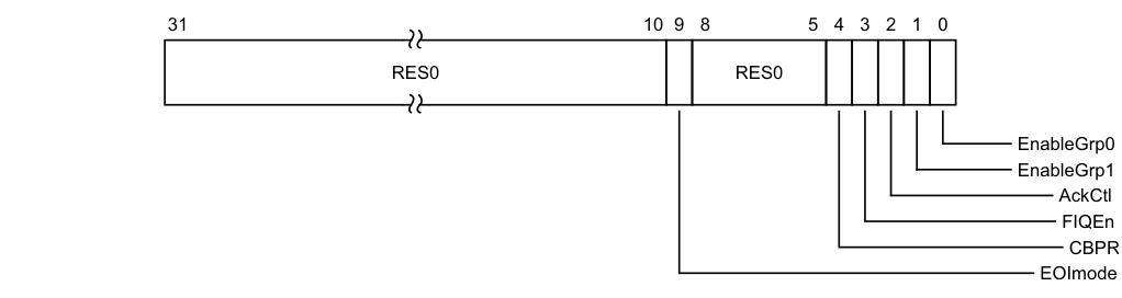
Image text
31 10 9 8 5 4 3 2 1 0
RES0 RES0
EnableGrp0
EnableGrp1
AckCtl
FIQEn
CBPR
EOImode
EOImode, bit [9]
Controls the behavior associated with the GICV_EOIR, GICV_AEOIR, and GICV_DIR registers:
0b0 Writes to GICV_EOIR and GICV_AEOIR perform priority drop and deactivate interrupt operations simultaneously. Behavior on a write to GICV_DIR is unpredictable.
When it has completed processing the interrupt, the virtual machine writes to GICV_EOIR or GICV_AEOIR to deactivate the interrupt. The write updates the List registers and causes the virtual CPU interface to signal the interrupt completion to the physical Distributor.
0b1 Writes to GICV_EOIR and GICV_AEOIR perform priority drop operation only. Writes to GICV_DIR perform deactivate interrupt operation only. When it has completed processing the interrupt, the virtual machine writes to GICV_DIR to deactivate the interrupt. The write updates the List registers and causes the virtual CPU interface to signal the interrupt completion to the Distributor.
On a Warm reset, this field resets to an architecturally UNKNOWN value.
Bits [8:5]
Reserved, RES0.
CBPR, bit [4]
Controls whether GICV_BPR affects both Group 0 and Group 1 interrupts:
0b0 GICV_BPR affects Group 0 virtual interrupts only. GICV_ABPR affects Group 1 virtual interrupts only. 0b1 GICV_BPR affects both Group 0 and Group 1 virtual interrupts. For more information, see Priority grouping. On a Warm reset, this field resets to an architecturally UNKNOWN value.
FIQEn, bit [3]
FIQ Enable. Controls whether Group 0 virtual interrupts are presented as virtual FIQs:
0b0 Group 0 virtual interrupts are presented as virtual IRQs. 0b1 Group 0 virtual interrupts are presented as virtual FIQs.
On a Warm reset, this field resets to an architecturally UNKNOWN value.
AckCtl, bit [2]
Arm deprecates use of this bit. Arm strongly recommends that software is written to operate with this bit always cleared to 0.
Acknowledge control. When the highest priority interrupt is Group 1, determines whether GICV_IAR causes the CPU interface to acknowledge the interrupt or returns the spurious identifier 1022, and whether GICV_HPPIR returns the interrupt ID or the special identifier 1022.
0b0 If the highest priority pending interrupt is Group 1, a read of GICV_IAR or GICV_HPPIR returns an interrupt ID of 1022.
0b1 If the highest priority pending interrupt is Group 1, a read of GICV_IAR or GICV_HPPIR returns the interrupt ID of the corresponding interrupt.
On a Warm reset, this field resets to an architecturally UNKNOWN value.
EnableGrp1, bit [1]
Enables the signaling of Group 1 virtual interrupts by the virtual CPU interface to the virtual machine:
0b0 Signaling of Group 1 interrupts is disabled. 0b1 Signaling of Group 1 interrupts is enabled.
On a Warm reset, this field resets to an architecturally UNKNOWN value.
EnableGrp0, bit [0]
Enables the signaling of Group 0 virtual interrupts by the virtual CPU interface to the virtual machine:
0b0 Signaling of Group 0 interrupts is disabled. 0b1 Signaling of Group 0 interrupts is enabled. On a Warm reset, this field resets to an architecturally UNKNOWN value.
Accessing the GICV_CTLR:
This register is used only when System register access is not enabled. When System register access is enabled:
-
For AArch32 implementations, ICC_CTLR provides equivalent functionality.
-
For AArch64 implementations, ICC_CTLR_EL1 provides equivalent functionality. GICV_CTLR can be accessed through its memory-mapped interface:
| Component | Offset | Instance |
|---|---|---|
| GIC Virtual CPU interface | 0x0000 | GICV_CTLR |
This interface is accessible as follows:
-
When GICD_CTLR.DS == 0 accesses to this register are RW.
-
When an access is Secure accesses to this register are RW.
-
When an access is Non-secure accesses to this register are RW.
12.15.8 GICV_DIR, Virtual Machine Deactivate Interrupt Register
The GICV_DIR characteristics are:
Purpose
Deactivates a specified virtual interrupt in the GICH_LR
Configurations
This register is available when the GIC implementation supports interrupt virtualization.
Attributes
GICV_DIR is a 32-bit register.
Field descriptions
The GICV_DIR bit assignments are:
| | 31 | | 25 | 24 | | 0 | | |—|—|—|—|—|—|—| |||||||||
Bits [31:25]
Reserved, RES0.
INTID, bits [24:0]
The INTID of the signaled interrupt.
Note
INTIDs 1020-1023 are reserved and convey additional information such as spurious interrupts.
When affinity routing is not enabled:
-
Bits [23:13] are RES0.
-
For SGIs, bits [12:10] identify the CPU interface corresponding to the source PE. For all other interrupts these bits are RES0.
When the virtual machine writes to this register, the specified interrupt in the List registers is changed from active to inactive, or from active and pending to pending. If the specified interrupt is present in the List registers but is not in either the active or active and pending states, the effect is UNPREDICTABLE. If the specified interrupt is not present in the List registers, GICH_HCR.EOICount is incremented, potentially generating a maintenance interrupt.
Note If the specified interrupt is not present in the List registers, the virtual machine cannot recover the INTID. Therefore, the hypervisor must ensure that, when GICV_CTLR.EOImode == 1, no more than one active interrupt is transferred from the List registers into a software list. If more than one active interrupt that is not stored in the List registers exists, the hypervisor must handle accesses to GICV_DIR in software, typically by trapping these accesses.
If the corresponding GICH_LR
Note Interrupt deactivation using this register is based on the provided INTID, with no requirement to deactivate interrupts in any particular order. A single register is therefore used to deactivate both Group 0 and Group 1 interrupts.
Accessing the GICV_DIR:
This register is used only when System register access is not enabled. When System register access is enabled:
-
For AArch32 implementations, ICC_DIR provides equivalent functionality.
-
For AArch64 implementations, ICC_DIR_EL1 provides equivalent functionality.
Writes to this register are valid only when GICV_CTLR.EOImode == 1. Writes to this register are otherwise UNPREDICTABLE.
When affinity routing is enabled, it is a programming error to use memory-mapped registers to access the GIC.
GICV_DIR can be accessed through its memory-mapped interface:
| Component | Offset | Instance |
|---|---|---|
| GIC Virtual CPU interface | 0x1000 | GICV_DIR |
This interface is accessible as follows:
-
When GICD_CTLR.DS == 0 accesses to this register are WO.
-
When an access is Secure accesses to this register are WO.
-
When an access is Non-secure accesses to this register are WO.
12.15.9 GICV_EOIR, Virtual Machine End Of Interrupt Register
The GICV_EOIR characteristics are:
Purpose
A write to this register performs a priority drop for the specified Group 0 virtual interrupt and, if GICV_CTLR.EOImode == 0, also deactivates the interrupt.
This register corresponds to the physical CPU interface register GICC_EOIR.
Configurations
This register is available when the GIC implementation supports interrupt virtualization.
Attributes
GICV_EOIR is a 32-bit register.
Field descriptions
The GICV_EOIR bit assignments are:
| | 31 | 25 | 24 | | 0 | | |—| RES0 | Reserved, RES0. |
INTID, bits [24:0]
The INTID of the signaled interrupt.
Note INTIDs 1020-1023 are reserved and convey additional information such as spurious interrupts.
When affinity routing is not enabled:
-
Bits [23:13] are RES0.
-
For SGIs, bits [12:10] identify the CPU interface corresponding to the source PE. For all other interrupts these bits are RES0.
The behavior of this register depends on the setting of GICV_CTLR.EOImode:
| GICV_CTLR.EOImode | Behavior |
|---|---|
| 0b0 | Both the priority drop and the deactivate interrupt effects occur |
| 0b1 | Only the priority drop effect occurs. |
A successful EOI request means that:
-
The highest priority bit in GICH_APR
is cleared, causing the running priority to drop. -
If the appropriate GICV_CTLR.EOImode bit == 0, the interrupt is deactivated in the corresponding List register GICH_LR
. If GICH_LR .HW == 1, indicating the INTID corresponds to a hardware interrupt, a deactivate request is also sent to the physical Distributor, identifying the physical INTID from the corresponding field in the List register. This effect is identical to a Non-secure write to GICC_DIR from the PE having that physical INTID. This means that if the corresponding physical interrupt is marked as Group 0, and GICD_CTLR.DS == 0, the deactivation request is ignored. See GICC_EOIR for more information.
Note Only Group 1 interrupts can target the hypervisor, and therefore only Group 1 interrupts are deactivated in the Distributor.
Accessing the GICV_EOIR:
This register is used only when System register access is not enabled. When System register access is enabled:
-
For AArch32 implementations, ICC_EOIR0 provides equivalent functionality.
-
For AArch64 implementations, ICC_EOIR0_EL1 provides equivalent functionality.
This register is used for Group 0 interrupts only. GICV_AEOIR provides equivalent functionality for Group 1 interrupts.
When affinity routing is enabled, it is a programming error to use memory-mapped registers to access the GIC.
GICV_EOIR can be accessed through its memory-mapped interface:
| Component | Offset | Instance |
|---|---|---|
| GIC Virtual CPU interface | 0x0010 | GICV_EOIR |
This interface is accessible as follows:
-
When GICD_CTLR.DS == 0 accesses to this register are WO.
-
When an access is Secure accesses to this register are WO.
-
When an access is Non-secure accesses to this register are WO.
12.15.10 GICV_HPPIR, Virtual Machine Highest Priority Pending Interrupt Register
The GICV_HPPIR characteristics are:
Purpose
Provides the INTID of the highest priority pending Group 0 virtual interrupt in the List registers. This register corresponds to the physical CPU interface register GICC_HPPIR.
Configurations
This register is available when the GIC implementation supports interrupt virtualization.
Attributes
GICV_HPPIR is a 32-bit register.
Field descriptions
The GICV_HPPIR bit assignments are:
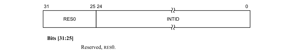
31 25 24 0
RES0 INTID
Bits [31:25]
Reserved, RES0.
INTID, bits [24:0]
The INTID of the signaled interrupt.
Note
INTIDs 1020-1023 are reserved and convey additional information such as spurious interrupts.
When affinity routing is not enabled:
-
Bits [23:13] are RES0.
-
For SGIs, bits [12:10] identify the CPU interface corresponding to the source PE. For all other interrupts these bits are RES0.
Reads of the GICC_HPPIR that do not return a valid INTID return a spurious INTID, 1022 or 1023. See Special INTIDs.
| GICV_CT | |||
|---|---|---|---|
| Highest priority pending interrupt Group | GICV_HPPIR read | LR.AckCt l | Returned INTID |
| 1 | Non-secure | x | ID of Group 1 interrupt |
| 1 | Secure | 0 | 1022 |
| 1 | Secure | 1 | ID of Group 1 interrupt |
| 0 | Non-secure | x | 1023 |
| 0 | Secure | x | ID of Group 0 interrupt |
| No pending interrupts | x | x | 1023 |
| If the CPU interface supports only a single Security state, the entries that apply to Secure reads describe the behavior. |
Accessing the GICV_HPPIR:
This register is used only when System register access is not enabled. When System register access is enabled:
-
For AArch32 implementations, ICC_HPPIR0 provides equivalent functionality.
-
For AArch64 implementations, ICC_HPPIR0_EL1 provides equivalent functionality.
This register is used for Group 0 interrupts only. GICV_AHPPIR provides equivalent functionality for Group 1 interrupts.
When affinity routing is enabled, it is a programming error to use memory-mapped registers to access the GIC.
GICV_HPPIR can be accessed through its memory-mapped interface:
Component Offset Instance GIC Virtual CPU interface 0x0018 GICV_HPPIR
This interface is accessible as follows:
-
When GICD_CTLR.DS == 0 accesses to this register are RO.
-
When an access is Secure accesses to this register are RO.
-
When an access is Non-secure accesses to this register are RO.
12.15.11 GICV_IAR, Virtual Machine Interrupt Acknowledge Register
The GICV_IAR characteristics are:
Purpose
Provides the INTID of the signaled Group 0 virtual interrupt. A read of this register by the PE acts as an acknowledge for the interrupt.
This register corresponds to the physical CPU interface register GICC_IAR.
Configurations
This register is available when the GIC implementation supports interrupt virtualization.
Attributes
GICV_IAR is a 32-bit register.
Field descriptions
The GICV_IAR bit assignments are:
| | 31 | | 25 | 24 | | 0 | | |—|—|—|—|—|—|—| |||||||||
Bits [31:25]
Reserved, RES0.
INTID, bits [24:0]
The INTID of the signaled interrupt.
Note
INTIDs 1020-1023 are reserved and convey additional information such as spurious interrupts.
When affinity routing is not enabled:
-
Bits [23:13] are RES0.
-
For SGIs, bits [12:10] identify the CPU interface corresponding to the source PE. For all other interrupts these bits are RES0.
When the virtual machine writes to this register, the virtual CPU interface acknowledges the highest priority pending virtual interrupt and sets the state in the corresponding List register to active. The appropriate bit in the active priorities register GICH_APR
If GICH_LR
A read of this register returns the spurious INTID 1023 if either of the following is true:
-
There are no pending interrupts of sufficiently high priority value to be signaled to the PE with the virtual CPU interface enabled and GICH_HCR.En == 1.
-
Interrupt signaling by the virtual CPU interface is disabled.
A read of this register returns the spurious INTID 1022 if the highest priority pending interrupt is Group 1 and GICV_CTLR.AckCtl == 0.
Accessing the GICV_IAR:
This register is used only when System register access is not enabled. When System register access is enabled:
-
For AArch32 implementations, ICC_IAR0 provides equivalent functionality.
-
For AArch64 implementations, ICC_IAR0_EL1 provides equivalent functionality.
This register is used for Group 0 interrupts only. GICV_AIAR provides equivalent functionality for Group 1 interrupts.
When affinity routing is enabled, it is a programming error to use memory-mapped registers to access the GIC.
GICV_IAR can be accessed through its memory-mapped interface:
| Component | Offset | Instance |
|---|---|---|
| GIC Virtual CPU interface | 0x000C | GICV_IAR |
This interface is accessible as follows:
-
When GICD_CTLR.DS == 0 accesses to this register are RO.
-
When an access is Secure accesses to this register are RO.
-
When an access is Non-secure accesses to this register are RO.
12.15.12 GICV_IIDR, Virtual Machine CPU Interface Identification Register
The GICV_IIDR characteristics are:
Purpose
Provides information about the implementer and revision of the virtual CPU interface.
Configurations
This register is available in all configurations of the GIC. If the GIC implementation supports two Security states this register is Common.
Attributes
GICV_IIDR is a 32-bit register.
Field descriptions
The GICV_IIDR bit assignments are:
| 31 20 19 16 15 12 11 0 | 31 20 19 16 15 12 11 0 | 31 20 19 16 15 12 11 0 | 31 20 19 16 15 12 11 0 | 31 20 19 16 15 12 11 0 |
|---|---|---|---|---|
| ProductID | Revision | Implementer | ||
Architecture_version
ProductID, bits [31:20]
An IMPLEMENTATION DEFINED product identifier.
Architecture_version, bits [19:16]
The version of the GIC architecture that is implemented.
0b0001 GICv1. 0b0010 GICv2. 0b0011 GICv3 memory-mapped interface supported. Support for the System register interface is discoverable from PE registers ID_PFR1 and ID_AA64PFR0_EL1. 0b0100 GICv4 memory-mapped interface supported. Support for the System register interface is discoverable from PE registers ID_PFR1 and ID_AA64PFR0_EL1.
Other values are reserved.
Revision, bits [15:12]
An IMPLEMENTATION DEFINED revision number for the CPU interface.
Implementer, bits [11:0]
Contains the JEP106 code of the company that implemented the CPU interface.
-
Bits [11:8] are the JEP106 continuation code of the implementer. For an Arm implementation, this field is 0x4.
-
Bit [7] is always 0.
-
Bits [6:0] are the JEP106 identity code of the implementer. For an Arm implementation, bits [7:0] are therefore 0x3B.
Accessing the GICV_IIDR:
GICV_IIDR can be accessed through its memory-mapped interface:
| Component | Offset | Instance |
|---|---|---|
| GIC Virtual CPU interface | 0x00FC | GICV_IIDR |
This interface is accessible as follows:
-
When GICD_CTLR.DS == 0 accesses to this register are RO.
-
When an access is Secure accesses to this register are RO.
-
When an access is Non-secure accesses to this register are RO.
12.15.13 GICV_PMR, Virtual Machine Priority Mask Register
The GICV_PMR characteristics are:
Purpose
This register provides a virtual interrupt priority filter. Only virtual interrupts with a higher priority than the value in this register are signaled to the PE.
Note
Higher interrupt priority corresponds to a lower value of the Priority field.
This register corresponds to the physical CPU interface register GICC_PMR.
Configurations
This register is available when the GIC implementation supports interrupt virtualization.
The Priority field of this register is aliased to GICH_VMCR.VMPR, to enable state to be switched easily between virtual machines during context-switching.
Attributes
GICV_PMR is a 32-bit register.
Field descriptions
The GICV_PMR bit assignments are:
| | 31 | | 8 | 7 | | 0 | | |—|—|— RES0 |—|—|— Priority |—|—| |||||||||
Bits [31:8]
Reserved, RES0.
Priority, bits [7:0]
The priority mask level for the virtual CPU interface. If the priority of the interrupt is higher than the value indicated by this field, the interface signals the interrupt to the PE.
If the GIC implementation supports fewer than 256 priority levels some bits might be RAZ/WI, as follows:
-
For 128 supported levels, bit [0] = 0b0.
-
For 64 supported levels, bits [1:0] = 0b00.
-
For 32 supported levels, bits [2:0] = 0b000.
-
For 16 supported levels, bits [3:0] = 0b0000.
For more information, see Interrupt prioritization.
On a Warm reset, this field resets to an architecturally UNKNOWN value.
Accessing the GICV_PMR:
This register is used only when System register access is not enabled. When System register access is enabled:
-
For AArch32 implementations, ICC_PMR provides equivalent functionality.
-
For AArch64 implementations, ICC_PMR_EL1 provides equivalent functionality. GICV_PMR can be accessed through its memory-mapped interface:
| Component | Offset | Instance |
|---|---|---|
| GIC Virtual CPU interface | 0x0004 | GICV_PMR |
This interface is accessible as follows:
-
When GICD_CTLR.DS == 0 accesses to this register are RW.
-
When an access is Secure accesses to this register are RW.
-
When an access is Non-secure accesses to this register are RW.
12.15.14 GICV_RPR, Virtual Machine Running Priority Register
The GICV_RPR characteristics are:
Purpose
This register indicates the running priority of the virtual CPU interface.
This register corresponds to the physical CPU interface register GICC_RPR.
Configurations
This register is available when the GIC implementation supports interrupt virtualization.
Attributes
GICV_RPR is a 32-bit register.
Field descriptions
The GICV_RPR bit assignments are:

31 8 7 0
RES0 Priority
Bits [31:8]
Reserved, RES0.
Priority, bits [7:0]
The current running priority on the virtual CPU interface. This is the group priority of the current active interrupt.
If there are no active interrupts on the CPU interface, or all active interrupts have undergone a priority drop, the value returned is the Idle priority.
The priority returned is the group priority as if the BPR was set to the minimum value.
Accessing the GICV_RPR:
This register is used only when System register access is not enabled. When System register access is enabled:
-
For AArch32 implementations, ICC_RPR provides equivalent functionality.
-
For AArch64 implementations, ICC_RPR_EL1 provides equivalent functionality.
Depending on the implementation, if no bits are set to 1 in GICH_APR
GICV_RPR can be accessed through its memory-mapped interface:
Component Offset Instance GIC Virtual CPU interface 0x0014 GICV_RPR
This interface is accessible as follows:
-
When GICD_CTLR.DS == 0 accesses to this register are RO.
-
When an access is Secure accesses to this register are RO.
-
When an access is Non-secure accesses to this register are RO.
12.15.15 GICV_STATUSR, Virtual Machine Error Reporting Status Register
The GICV_STATUSR characteristics are:
Purpose
Provides software with a mechanism to detect:
-
Accesses to reserved locations.
-
• Writes to read-only locations.
-
Reads of write-only locations.
Configurations
In systems where this register is implemented, Arm expects that when a virtual machine is scheduled, the hypervisor ensures that this register is cleared to 0. The hypervisor might check for illegal accesses when the virtual machine is unscheduled.
Attributes
GICV_STATUSR is a 32-bit register.
Field descriptions
The GICV_STATUSR bit assignments are:

Image text
31 4 3 2 1 0
RES0
RRD
WRD
RWOD
WROD
WROD, bit [3]
Write to an RO location. 0b0 Normal operation. 0b1 A write to an RO location has been detected. When a violation is detected, software must write 1 to this register to reset it.
RWOD, bit [2]
Read of a WO location. 0b0 Normal operation. 0b1 A read of a WO location has been detected. When a violation is detected, software must write 1 to this register to reset it.
WRD, bit [1]
Write to a reserved location. 0b0 Normal operation. 0b1 A write to a reserved location has been detected. When a violation is detected, software must write 1 to this register to reset it.
RRD, bit [0]
Read of a reserved location.
0b0 Normal operation. 0b1 A read of a reserved location has been detected. When a violation is detected, software must write 1 to this register to reset it.
Accessing the GICV_STATUSR:
This is an optional register. If the register is implemented, GICC_STATUSR must also be implemented. If the register is not implemented, the location is RAZ/WI.
This register is used only when System register access is not enabled. If System register access is enabled, this register is not updated. Equivalent function might be provided by appropriate traps and exceptions.
GICV_STATUSR can be accessed through its memory-mapped interface:
Component Offset Instance GIC Virtual CPU interface 0x002C GICV_STATUSR
This interface is accessible as follows:
-
When GICD_CTLR.DS == 0 accesses to this register are RW.
-
When an access is Secure accesses to this register are RW.
-
When an access is Non-secure accesses to this register are RW.
12.16 The GIC virtual interface control register map
The GIC virtual interface control registers are management registers. Configuration software on the PE must ensure they are accessible only by a hypervisor, or similar software.
Reserved register addresses are RES0.
Table 12-32 shows the register map for the GIC virtual interface control registers.
Table 12-32 GIC virtual interface control register map
| Offset | Name | Type | Reset | Description |
|---|---|---|---|---|
| 0x0000 | GICH_HCR | RW | 0x00000000 | Hypervisor Control Register |
| 0x0004 | GICH_VTR | RO | IMPLEMENTATION DEFINED | VGIC Type Register |
| 0x0008 | GICH_VMCR | RW | - | Virtual Machine Control Register |
| 0x000C | - | - | - | Reserved |
| 0x0010 | GICH_MISR | RO | 0x00000000 | Maintenance Interrupt Status Register |
| 0x0014-0x001C | - | - | - | Reserved |
| 0x0020 | GICH_EISR | RO | 0x00000000 | End of Interrupt Status Register |
| 0x0024-0x002C | - | - | - | Reserved |
| 0x0030 | GICH_ELRSR | RO | IMPLEMENTATION DEFINEDa | Empty List Register Status Register |
| 0x0034-0x00EC | - | - | - | Reserved |
| 0x00F0-0x00FC | GICH_APR | RW | 0x00000000 | Active Priorities Register |
| 0x0100-0x013C | GICH_LR | RW | 0x00000000 | List Registers 0-15 lower bits |
- a. Each bit that has a corresponding List register resets to 1, meaning that the reset value of the register depends on the number of List registers implemented.
Note It is IMPLEMENTATION DEFINED whether an access to a GIC virtual interface control register using the memory-mapped interface accesses the same state as an access using the System register interface, or whether the two interfaces access different states.
12.17 The GIC virtual interface control register descriptions
This section describes each of the GIC virtual interface control registers in register name order.
12.17.1 GICH_APR, Active Priorities Registers, n = 0 - 3
The GICH_APR
Purpose
These registers track which preemption levels are active in the virtual CPU interface, and indicate the current active priority. Corresponding bits are set to 1 in this register when an interrupt is acknowledged, based on GICH_LR
Configurations
This register is available when the GIC implementation supports interrupt virtualization.
The number of registers required depends on how many bits are implemented in GICH_LR
-
When 5 priority bits are implemented, 1 register is required (GICH_APR0).
-
When 6 priority bits are implemented, 2 registers are required (GICH_APR0, GICH_APR1).
-
When 7 priority bits are implemented, 4 registers are required (GICH_APR0, GICH_APR1, GICH_APR2, GICH_APR3).
Unimplemented registers are RAZ/WI.
Attributes
GICH_APR
Field descriptions
The GICH_APR
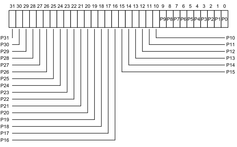
Image text
31 30 29 28 27 26 25 24 23 22 21 20 19 18 17 16 15 14 13 12 11 10 9 8 7 6 5 4 3 2 1 0
P9 P8 P7 P6 P5 P4 P3 P2 P1 P0
P31 P10
P30 P11
P29 P12
P28 P13
P27 P14
P26 P15
P25
P24
P23
P22
P21
P20
P19
P18
P17
P16
-
0b0 There is no interrupt active at the priority corresponding to that bit.
-
0b1 There is an interrupt active at the priority corresponding to that bit.
The correspondence between priorities and bits depends on the number of bits of priority that are implemented. If 5 bits of priority are implemented (bits [7:3] of priority), then there are 32 priority groups, and the active state of these priorities are held in GICH_APR0 in the bits corresponding to Priority[7:3].
If 6 bits of priority are implemented (bits [7:2] of priority), then there are 64 priority groups, and:
-
The active state of priorities 0 - 124 are held in GICH_APR0 in the bits corresponding to 0:Priority[6:2].
-
The active state of priorities 128 - 252 are held in GICH_APR1 in the bits corresponding to 1:Priority[6:2].
If 7 bits of priority are implemented (bits [7:1] of priority), then there are 128 priority groups, and:
-
The active state of priorities 0 - 62 are held in GICH_APR0 in the bits corresponding to 00:Priority[5:1].
-
The active state of priorities 64 - 126 are held in GICH_APR1 in the bits corresponding to 01:Priority[5:1].
-
The active state of priorities 128 - 190 are held in GICH_APR2 in the bits corresponding to 10:Priority[5:1].
-
The active state of priorities 192 - 254 are held in GICH_APR3 in the bits corresponding to 11:Priority[5:1].
On a Warm reset, this field resets to 0.
Accessing the GICH_APR:
These registers are used only when System register access is not enabled. When System register access is enabled the following registers provide equivalent functionality:
-
In AArch64:
- For Group 0, ICH_AP0R<n>_EL2.- For Group 1, ICH_AP1R
_EL2.
- For Group 1, ICH_AP1R
-
In AArch32:
-
For Group 0, ICH_AP0R
. -
For Group 1, ICH_AP1R
.
-
GICH_APR
| Component | Offset | Instance |
|---|---|---|
| GIC Virtual interface control | 0x00F0+ (4 * n) | GICH_APR |
This interface is accessible as follows:
-
When GICD_CTLR.DS == 0 accesses to this register are RW.
-
When an access is Secure accesses to this register are RW.
-
When an access is Non-secure accesses to this register are RW.
12.17.2 GICH_EISR, End Interrupt Status Register
The GICH_EISR characteristics are:
Purpose
Indicates which List registers have outstanding EOI maintenance interrupts.
Configurations
This register is available when the GIC implementation supports interrupt virtualization.
Attributes
GICH_EISR is a 32-bit register.
Field descriptions
The GICH_EISR bit assignments are:

Image text
31 16 15 14 13 12 11 10 9 8 7 6 5 4 3 2 1 0
RES0
Status15 Status0
Status1
Status2
Status3
Status4
Status5
Status6
Status7
Status8
Status9
Status10
Status11
Status12
Status13
Status14
Reserved, RES0.
Status, bit [n], for n = 15 to 0
EOI maintenance interrupt status for List register
-
0b0 GICH_LR
does not have an EOI maintenance interrupt. -
0b1 GICH_LR
has an EOI maintenance interrupt that has not been handled.
For any GICH_LR
-
GICH_LR
.State is 0b00. -
GICH_LR
.HW == 0. -
GICH_LR
.EOI == 1.
On a Warm reset, this field resets to an architecturally UNKNOWN value.
Accessing the GICH_EISR:
This register is used only when System register access is not enabled. When System register access is enabled:
-
For AArch32 implementations, ICH_EISR provides equivalent functionality.
-
For AArch64 implementations, ICH_EISR_EL2 provides equivalent functionality.
Bits corresponding to unimplemented List registers are RAZ.
GICH_EISR can be accessed through its memory-mapped interface:
Component Offset Instance GIC Virtual interface control 0x0020 GICH_EISR
This interface is accessible as follows:
-
When GICD_CTLR.DS == 0 accesses to this register are RO.
-
When an access is Secure accesses to this register are RO.
-
When an access is Non-secure accesses to this register are RO.
12.17.3 GICH_ELRSR, Empty List Register Status Register
The GICH_ELRSR characteristics are:
Purpose
Indicates which List registers contain valid interrupts.
Configurations
This register is available when the GIC implementation supports interrupt virtualization.
Attributes
GICH_ELRSR is a 32-bit register.
Field descriptions
The GICH_ELRSR bit assignments are:
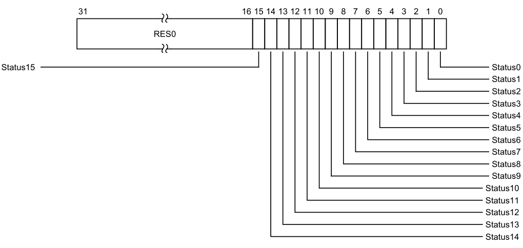
Image text
31 16 15 14 13 12 11 10 9 8 7 6 5 4 3 2 1 0
RES0
Status15 Status0
Status1
Status2
Status3
Status4
Status5
Status6
Status7
Status8
Status9
Status10
Status11
Status12
Status13
Status14
Reserved, RES0.
Status, bit [n], for n = 15 to 0
Status bit for List register
- 0b0 GICH_LR
, if implemented, contains a valid interrupt. Using this List register can result in overwriting a valid interrupt.
0b1 GICH_LR
For any GICH_LR
-
GICH_LR
.HW == 1. -
GICH_LR
.EOI == 0.
On a Warm reset, this field resets to 1.
Accessing the GICH_ELRSR:
This register is used only when System register access is not enabled. When System register access is enabled:
-
For AArch32 implementations, ICH_ELRSR provides equivalent functionality.
-
For AArch64 implementations, ICH_ELRSR_EL2 provides equivalent functionality.
Bits corresponding to unimplemented List registers are RES0.
GICH_ELRSR can be accessed through its memory-mapped interface:
Component Offset Instance GIC Virtual interface control 0x0030 GICH_ELRSR
This interface is accessible as follows:
-
When GICD_CTLR.DS == 0 accesses to this register are RO.
-
When an access is Secure accesses to this register are RO.
-
When an access is Non-secure accesses to this register are RO.
12.17.4 GICH_HCR, Hypervisor Control Register
The GICH_HCR characteristics are:
Purpose
Controls the virtual CPU interface.
Configurations
This register is available when the GIC implementation supports interrupt virtualization.
Attributes
GICH_HCR is a 32-bit register.
Field descriptions
The GICH_HCR bit assignments are:
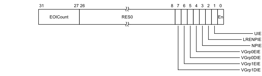
Image text
31 27 26 8 7 6 5 4 3 2 1 0
EOICount RES0 En
UIE
LRENPIE
NPIE
VGrp0EIE
VGrp0DIE
VGrp1EIE
VGrp1DIE
The maintenance interrupt is asserted whenever this field is nonzero and GICH_HCR.LRENPIE == 1.
On a Warm reset, this field resets to an architecturally UNKNOWN value.
Bits [26:8]
Reserved, RES0.
VGrp1DIE, bit [7]
VM Group 1 Disabled Interrupt Enable.
Enables the signaling of a maintenance interrupt while signaling of Group 1 interrupts from the virtual CPU interface to the connected virtual machine is disabled:
0b0 Maintenance interrupt disabled. 0b1 Maintenance interrupt signaled when GICV_CTLR.EnableGrp1 == 0.
On a Warm reset, this field resets to an architecturally UNKNOWN value.
VGrp1EIE, bit [6]
VM Group 1 Enabled Interrupt Enable. Enables the signaling of a maintenance interrupt while signaling of Group 1 interrupts from the virtual CPU interface to the connected virtual machine is enabled:
0b0 Maintenance interrupt disabled. 0b1 Maintenance interrupt signaled when GICV_CTLR.EnableGrp1 == 1. On a Warm reset, this field resets to an architecturally UNKNOWN value.
VGrp0DIE, bit [5]
VM Group 0 Disabled Interrupt Enable. Enables the signaling of a maintenance interrupt while signaling of Group 0 interrupts from the virtual CPU interface to the connected virtual machine is disabled: 0b0 Maintenance interrupt disabled. 0b1 Maintenance interrupt signaled when GICV_CTLR.EnableGrp0 == 0. On a Warm reset, this field resets to an architecturally UNKNOWN value.
VGrp0EIE, bit [4]
VM Group 0 Enabled Interrupt Enable. Enables the signaling of a maintenance interrupt while signaling of Group 0 interrupts from the virtual CPU interface to the connected virtual machine is enabled: 0b0 Maintenance interrupt disabled. 0b1 Maintenance interrupt signaled when GICV_CTLR.EnableGrp0 == 1. On a Warm reset, this field resets to an architecturally UNKNOWN value.
NPIE, bit [3]
No Pending Interrupt Enable.
Enables the signaling of a maintenance interrupt while no pending interrupts are present in the List registers: 0b0 Maintenance interrupt disabled. 0b1 Maintenance interrupt signaled while the List registers contain no interrupts in the pending state.
On a Warm reset, this field resets to an architecturally UNKNOWN value.
LRENPIE, bit [2]
List Register Entry Not Present Interrupt Enable.
Enables the signaling of a maintenance interrupt while the virtual CPU interface does not have a corresponding valid List register for an EOI request:
0b0 Maintenance interrupt disabled. 0b1 Maintenance interrupt signaled while GICH_HCR.EOICount is not 0.
On a Warm reset, this field resets to an architecturally UNKNOWN value.
UIE, bit [1]
Underflow Interrupt Enable.
Enables the signaling of a maintenance interrupt when the List registers are either empty or hold only one valid entry.
0b0 Maintenance interrupt disabled. 0b1 A maintenance interrupt is signaled if zero or one of the List register entries are marked as a valid interrupt.
On a Warm reset, this field resets to an architecturally UNKNOWN value.
En, bit [0]
Enable. Global enable bit for the virtual CPU interface.
0b0 Virtual CPU interface operation is disabled. 0b1 Virtual CPU interface operation is enabled.
When this field is 0:
-
The virtual CPU interface does not signal any maintenance interrupts.
-
The virtual CPU interface does not signal any virtual interrupts.
-
A read of GICV_IAR or GICV_AIAR returns a spurious interrupt ID.
On a Warm reset, this field resets to an architecturally UNKNOWN value.
The VGrp1DIE, VGrp1EIE, VGrp0DIE, and VGrp0EIE fields permit the hypervisor to track the virtual CPU interfaces that are enabled. The hypervisor can then route interrupts that have multiple targets correctly and efficiently, without having to read the virtual CPU interface status.
See Maintenance interrupts and GICH_MISR for more information.
Accessing the GICH_HCR:
This register is used only when System register access is not enabled. When System register access is enabled:
-
For AArch32 implementations, ICH_HCR provides equivalent functionality.
-
For AArch64 implementations, ICH_HCR_EL2 provides equivalent functionality.
GICH_HCR.En must be set to 1 for any virtual or maintenance interrupt to be asserted.
GICH_HCR can be accessed through its memory-mapped interface:
Component Offset Instance GIC Virtual interface control 0x0000 GICH_HCR
This interface is accessible as follows:
-
When GICD_CTLR.DS == 0 accesses to this register are RW.
-
When an access is Secure accesses to this register are RW.
-
When an access is Non-secure accesses to this register are RW.
12.17.5 GICH_LR, List Registers, n = 0 - 15
The GICH_LR
Purpose
These registers provide context information for the virtual CPU interface.
Configurations
This register is available when the GIC implementation supports interrupt virtualization.
A maximum of 16 List registers can be provided. GICH_VTR.ListRegs defines the number implemented. Unimplemented List registers are RAZ/WI.
Attributes
GICH_LR
Field descriptions
The GICH_LR
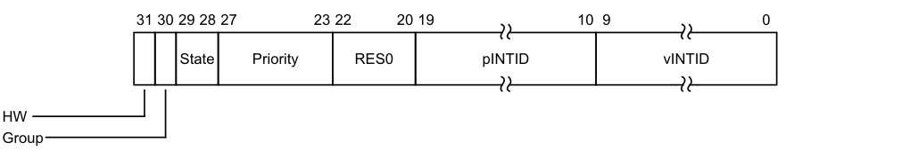
31 30 29 28 27 23 22 20 19 10 9 0
State Priority RES0 pINTID vINTID
HW
Group
HW, bit [31]
Indicates whether this virtual interrupt is a hardware interrupt, meaning that it corresponds to a physical interrupt. Deactivation of the virtual interrupt also causes the deactivation of the physical interrupt corresponding to the INTID:
0b0 This interrupt is triggered entirely in software. No notification is sent to the Distributor when the virtual interrupt is deactivated.
- 0b1 A hardware interrupt. A deactivate interrupt request is sent to the Distributor when the virtual interrupt is deactivated, using GICH_LR
.pINTID to indicate the physical interrupt identifier.
If GICV_CTLR.EOImode == 0, this request corresponds to a write to GICV_EOIR or GICV_AEOIR, otherwise it corresponds to a write to GICV_DIR.
On a Warm reset, this field resets to an architecturally UNKNOWN value.
Group, bit [30]
Indicates whether the interrupt is Group 0 or Group 1:
0b0 Group 0 virtual interrupt. GICV_CTLR.FIQEn determines whether it is signaled as a virtual IRQ or as a virtual FIQ, and GICV_CTLR.EnableGrp0 enables signaling of this interrupt to the virtual machine. 0b1 Group 1 virtual interrupt, signaled as a virtual IRQ. GICV_CTLR.EnableGrp1 enables signaling of this interrupt to the virtual machine.
Note GICV_CTLR.CBPR controls whether GICV_BPR or GICV_ABPR determines if a pending Group 1 interrupt has sufficient priority to preempt current execution.
On a Warm reset, this field resets to an architecturally UNKNOWN value.
State, bits [29:28]
The state of the interrupt. This field has one of the following values:
0b00 Inactive 0b01 Pending 0b10 Active 0b11 Active and pending
The GIC updates these state bits as virtual interrupts proceed through the interrupt life cycle. Entries in the inactive state are ignored, except for the purpose of generating virtual maintenance interrupts.
Note For hardware interrupts, the active and pending state is held in the Distributor rather than the virtual CPU interface. A hypervisor must only use the active and pending state for software originated interrupts, which are typically associated with virtual devices, or for SGIs.
On a Warm reset, this field resets to an architecturally UNKNOWN value.
Priority, bits [27:23]
The priority of this interrupt.
On a Warm reset, this field resets to an architecturally UNKNOWN value.
Bits [22:20]
Reserved, RES0.
pINTID, bits [19:10]
The function of this field depends on the value of GICH_LR
When GICH_LR
-
Bit [19] indicates whether the interrupt triggers an EOI maintenance interrupt. If this bit is 1, then when the interrupt identified by vINTID is deactivated, an EOI maintenance interrupt is asserted.
-
Bits [18:13] are reserved, SBZ.
-
If the vINTID field value corresponds to an SGI (that is, 0-15), bits [12:10] contain the number of the requesting PE. This appears in the corresponding field of GICV_IAR or GICV_AIAR. If the vINTID field value is not 0-15, this field must be cleared to 0.
When GICH_LR
-
This field indicates the pINTID that the hypervisor forwards to the Distributor. This field is only required to implement enough bits to hold a valid value for the ID configuration. Any unused higher order bits are RAZ/WI.
-
If the value of pINTID is 0-15 or 1020-1023, behavior is UNPREDICTABLE. If the value of pINTID is 16-31, this field applies to the PPI associated with this same PE as the virtual CPU interface requesting the deactivation.
On a Warm reset, this field resets to an architecturally UNKNOWN value.
vINTID, bits [9:0]
This INTID is returned to the VM when the interrupt is acknowledged through GICV_IAR. Each valid interrupt stored in the List registers must have a unique vINTID for that virtual CPU interface. If the value of vINTID is 1020-1023, behavior is UNPREDICTABLE.
On a Warm reset, this field resets to an architecturally UNKNOWN value.
Accessing the GICH_LR:
This register is used only when System register access is not enabled. When System register access is enabled:
- For AArch32 implementations, ICH_LR
provides equivalent functionality. - For AArch64 implementations, ICH_LR
_EL2 provides equivalent functionality.
GICH_LR
| Component | Offset | Instance |
|---|---|---|
| GIC Virtual interface control | 0x0100+ (4 * n) | GICH_LR |
This interface is accessible as follows:
-
When GICD_CTLR.DS == 0 accesses to this register are RW.
-
When an access is Secure accesses to this register are RW.
-
When an access is Non-secure accesses to this register are RW.
12.17.6 GICH_MISR, Maintenance Interrupt Status Register
The GICH_MISR characteristics are:
Purpose
Indicates which maintenance interrupts are asserted.
Configurations
This register is available when the GIC implementation supports interrupt virtualization.
Attributes
GICH_MISR is a 32-bit register.
Field descriptions
The GICH_MISR bit assignments are:
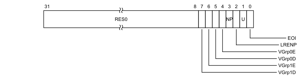
Image text
31 8 7 6 5 4 3 2 1 0
RES0 NP U
EOI
LRENP
VGrp0E
VGrp0D
VGrp1E
VGrp1D
VGrp1D, bit [7]
vPE Group 1 Disabled.
0b0 vPE Group 1 Disabled maintenance interrupt not asserted. 0b1 vPE Group 1 Disabled maintenance interrupt asserted.
This maintenance interrupt is asserted when GICH_HCR.VGrp1DIE == 1 and GICH_VMCR.VENG1 == 0.
On a Warm reset, this field resets to 0.
VGrp1E, bit [6]
vPE Group 1 Enabled.
0b0 vPE Group 1 Enabled maintenance interrupt not asserted. 0b1 vPE Group 1 Enabled maintenance interrupt asserted. This maintenance interrupt is asserted when GICH_HCR.VGrp1EIE == 1 and GICH_VMCR.VENG1 == 1.
On a Warm reset, this field resets to 0.
VGrp0D, bit [5]
vPE Group 0 Disabled. 0b0 vPE Group 0 Disabled maintenance interrupt not asserted. 0b1 vPE Group 0 Disabled maintenance interrupt asserted. This maintenance interrupt is asserted when GICH_HCR.VGrp0DIE == 1 and GICH_VMCR.VENG0 == 0.
On a Warm reset, this field resets to 0.
VGrp0E, bit [4]
vPE Group 0 Enabled.
0b0 vPE Group 0 Enabled maintenance interrupt not asserted. 0b1 vPE Group 0 Enabled maintenance interrupt asserted. This maintenance interrupt is asserted when GICH_HCR.VGrp0EIE == 1 and GICH_VMCR.VENG0 == 1.
On a Warm reset, this field resets to 0.
NP, bit [3]
No Pending.
0b0 No Pending maintenance interrupt not asserted. 0b1 No Pending maintenance interrupt asserted. This maintenance interrupt is asserted when GICH_HCR.NPIE == 1 and no List register is in the pending state.
On a Warm reset, this field resets to 0.
LRENP, bit [2]
List Register Entry Not Present.
0b0 List Register Entry Not Present maintenance interrupt not asserted. 0b1 List Register Entry Not Present maintenance interrupt asserted. This maintenance interrupt is asserted when GICH_HCR.LRENPIE == 1 and GICH_HCR.EOICount is nonzero.
On a Warm reset, this field resets to 0.
U, bit [1]
Underflow.
0b0 Underflow maintenance interrupt not asserted. 0b1 Underflow maintenance interrupt asserted.
This maintenance interrupt is asserted when GICH_HCR.UIE == 1 and zero or one of the List register entries are marked as a valid interrupt.
On a Warm reset, this field resets to 0.
EOI, bit [0]
End Of Interrupt. 0b0 End Of Interrupt maintenance interrupt not asserted. 0b1 End Of Interrupt maintenance interrupt asserted. This maintenance interrupt is asserted when at least one bit in GICH_EISR == 1. On a Warm reset, this field resets to 0.
Note A List register is in the pending state only if the corresponding GICH_LR
value is 0b01, that is, pending. The active and pending state is not included.
Accessing the GICH_MISR:
This register is used only when System register access is not enabled. When System register access is enabled:
-
For AArch32 implementations, ICH_MISR provides equivalent functionality.
-
For AArch64 implementations, ICH_MISR_EL2 provides equivalent functionality.
A maintenance interrupt is asserted only if at least one bit is set to 1 in this register and if GICH_HCR.En == 1.
GICH_MISR can be accessed through its memory-mapped interface:
| Component | Offset | Instance |
|---|---|---|
| GIC Virtual interface control | 0x0010 | GICH_MISR |
This interface is accessible as follows:
-
When GICD_CTLR.DS == 0 accesses to this register are RO.
-
When an access is Secure accesses to this register are RO.
-
When an access is Non-secure accesses to this register are RO.
12.17.7 GICH_VMCR, Virtual Machine Control Register
The GICH_VMCR characteristics are:
Purpose
Enables the hypervisor to save and restore the virtual machine view of the GIC state. This register is updated when a virtual machine updates the virtual CPU interface registers.
Configurations
This register is available when the GIC implementation supports interrupt virtualization.
Attributes
GICH_VMCR is a 32-bit register.
Field descriptions
The GICH_VMCR bit assignments are:
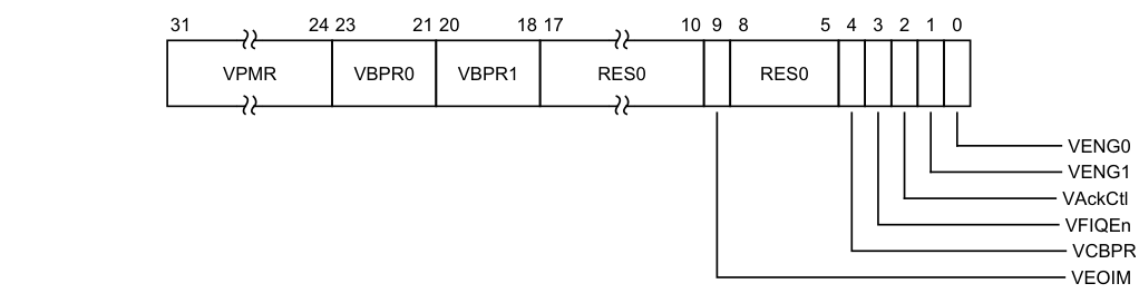
Image text
31 24 23 21 20 18 17 10 9 8 5 4 3 2 1 0
VPMR VBPR0 VBPR1 RES0 RES0
VENG0
VENG1
VAckCtl
VFIQEn
VCBPR
VEOIM
This alias field is updated when a VM updates GICV_PMR.Priority.
On a Warm reset, this field resets to an architecturally UNKNOWN value.
VBPR0, bits [23:21]
Virtual Binary Point Register, Group 0. Defines the point at which the priority value fields split into two parts, the Group priority field and the subpriority field. The Group priority field determines Group 0 interrupt preemption, and also determines Group 1 interrupt preemption if GICH_VMCR.VCBPR == 1.
This alias field is updated when a VM updates GICV_BPR.Binary_Point.
On a Warm reset, this field resets to an architecturally UNKNOWN value.
VBPR1, bits [20:18]
Virtual Binary Point Register, Group 1. Defines the point at which the priority value fields split into two parts, the Group priority field and the subpriority field. The Group priority field determines Group 1 interrupt preemption if GICH_VMCR.VCBPR == 0.
This alias field is updated when a VM updates GICV_ABPR.Binary_Point.
On a Warm reset, this field resets to an architecturally UNKNOWN value.
Bits [17:10]
Reserved, RES0.
VEOIM, bit [9]
Virtual EOImode. Possible values of this bit are:
0b0 A write of an INTID to GICV_EOIR or GICV_AEOIR drops the priority of the interrupt with that INTID, and also deactivates that interrupt. 0b1 A write of an INTID to GICV_EOIR or GICV_AEOIR only drops the priority of the interrupt with that INTID. Software must write to GICV_DIR to deactivate the interrupt. This alias field is updated when a VM updates GICV_CTLR.EOImode. On a Warm reset, this field resets to an architecturally UNKNOWN value.
Bits [8:5]
Reserved, RES0.
VCBPR, bit [4]
Virtual Common Binary Point Register. Possible values of this bit are: 0b0 GICV_ABPR determines the preemption group for Group 1 interrupts. 0b1 GICV_BPR determines the preemption group for Group 1 interrupts. This alias field is updated when a VM updates GICV_CTLR.CBPR. On a Warm reset, this field resets to an architecturally UNKNOWN value.
VFIQEn, bit [3]
Virtual FIQ enable. Possible values of this bit are:
0b0 Group 0 virtual interrupts are presented as virtual IRQs. 0b1 Group 0 virtual interrupts are presented as virtual FIQs. This alias field is updated when a VM updates GICV_CTLR.FIQEn. On a Warm reset, this field resets to an architecturally UNKNOWN value.
VAckCtl, bit [2]
Virtual AckCtl. Possible values of this bit are:
0b0 If the highest priority pending interrupt is Group 1, a read of GICV_IAR or GICV_HPPIR returns an INTID of 1022. 0b1 If the highest priority pending interrupt is Group 1, a read of GICV_IAR or GICV_HPPIR returns the INTID of the corresponding interrupt. This alias field is updated when a VM updates GICV_CTLR.AckCtl. This field is supported for backwards compatibility with GICv2. Arm deprecates the use of this field.
On a Warm reset, this field resets to an architecturally UNKNOWN value.
VENG1, bit [1]
Virtual interrupt enable, Group 1. Possible values of this bit are:
0b0 Group 1 virtual interrupts are disabled. 0b1 Group 1 virtual interrupts are enabled. This alias field is updated when a VM updates GICV_CTLR.EnableGrp1. On a Warm reset, this field resets to an architecturally UNKNOWN value.
VENG0, bit [0]
Virtual interrupt enable, Group 0. Possible values of this bit are:
0b0 Group 0 virtual interrupts are disabled. 0b1 Group 0 virtual interrupts are enabled. This alias field is updated when a VM updates GICV_CTLR.EnableGrp0. On a Warm reset, this field resets to an architecturally UNKNOWN value.
Note A List register is in the pending state only if the corresponding GICH_LR
value is 0b01, that is, pending. The active and pending state is not included.
Accessing the GICH_VMCR:
This register is used only when System register access is not enabled. When System register access is enabled:
-
For AArch32 implementations, ICH_VMCR provides equivalent functionality.
-
For AArch64 implementations, ICH_VMCR_EL2 provides equivalent functionality.
GICH_VMCR can be accessed through its memory-mapped interface:
| Component | Offset | Instance |
|---|---|---|
| GIC Virtual interface control | 0x0008 | GICH_VMCR |
This interface is accessible as follows:
-
When GICD_CTLR.DS == 0 accesses to this register are RW.
-
When an access is Secure accesses to this register are RW.
-
When an access is Non-secure accesses to this register are RW.
12.17.8 GICH_VTR, Virtual Type Register
The GICH_VTR characteristics are:
Purpose
Indicates the number of implemented virtual priority bits and List registers.
Configurations
This register is available when the GIC implementation supports interrupt virtualization.
Attributes
GICH_VTR is a 32-bit register.
Field descriptions
The GICH_VTR bit assignments are:
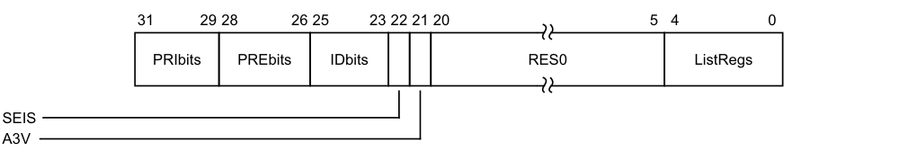
31 29 28 26 25 23 22 21 20 5 4 0
PRIbits PREbits IDbits RES0 ListRegs
SEIS
A3V
PRIbits, bits [31:29]
The number of virtual priority bits implemented, minus one.
An implementation must implement at least 32 levels of virtual priority (5 priority bits).
PREbits, bits [28:26]
The number of virtual preemption bits implemented, minus one.
An implementation must implement at least 32 levels of virtual preemption priority (5 preemption bits).
The value of this field must be less than or equal to the value of GICH_VTR.PRIbits.
IDbits, bits [25:23]
The number of virtual interrupt identifier bits supported:
0b000 16 bits. 0b001 24 bits. All other values are reserved.
SEIS, bit [22]
SEI support. Indicates whether the virtual CPU interface supports generation of SEIs:
0b0 The virtual CPU interface logic does not support generation of SEIs. 0b1 The virtual CPU interface logic supports generation of SEIs.
A3V, bit [21]
Affinity 3 valid. Possible values are:
0b0 The virtual CPU interface logic only supports zero values of the Aff3 field in ICC_SGI0R_EL1, ICC_SGI1R_EL1, and ICC_ASGI1R_EL1. 0b1 The virtual CPU interface logic supports nonzero values of the Aff3 field in ICC_SGI0R_EL1, ICC_SGI1R_EL1, and ICC_ASGI1R_EL1.
Bits [20:5]
Reserved, RES0.
ListRegs, bits [4:0]
The number of implemented List registers, minus one.
Accessing the GICH_VTR:
This register is used only when System register access is not enabled. When System register access is enabled:
-
For AArch32 implementations, ICH_VTR provides equivalent functionality.
-
For AArch64 implementations, ICH_VTR_EL2 provides equivalent functionality.
GICH_VTR can be accessed through its memory-mapped interface:
| Component | Offset | Instance |
|---|---|---|
| GIC Virtual interface control | 0x0004 | GICH_VTR |
This interface is accessible as follows:
-
When GICD_CTLR.DS == 0 accesses to this register are RO.
-
When an access is Secure accesses to this register are RO.
-
When an access is Non-secure accesses to this register are RO.
12.18 The ITS register map
The ITS address map consists of two separate 64KB frames starting from an IMPLEMENTATION DEFINED address specified in ITS_base. This base address must be aligned to a 64KB boundary. The two frames are:
-
The control registers. which are located at ITS_base + 0x000000.
-
The interrupt translation space, which is located at ITS_base + 0x010000.
-
The virtual SGI space, which is located at ITS_base + 0x020000 (GICv4.1).
Reserved register addresses are RES0.
Table 12-33 shows the GIC register map for the ITS control registers.
Table 12-33 ITS control register map
| Offset | Name | Type | Reset | Description |
|---|---|---|---|---|
| 0x0000 | GITS_CTLR | RW | See the register description | ITS control register |
| 0x0004 | GITS_IIDR | RO | IMPLEMENTATION DEFINED | ITS Identification register |
| 0x0008 | GITS_TYPER | RO | IMPLEMENTATION DEFINED | ITS Type register |
| 0x0010 | GITS_MPAMIDR | RO | IMPLEMENTATION DEFINED | ITS supported MPAM sizes |
| 0x0014 | GITS_PARTIDR | RW | 0 | ITS PARTID register |
| 0x0018 | GITS_MPIDR | RO | IMPLEMENTATION DEFINED | ITS affinity |
| 0x001C | - | - | - | Reserved |
| 0x0020-0x003C | - | - | IMPLEMENTATION DEFINED | IMPLEMENTATION DEFINEDregisters. |
| 0x0040 | GITS_STATUSR | RW | 0X0000 0000 | ITS Error Reporting Status Register, optional |
| 0x0044 | - | - | - | Reserved |
| 0x0048 | GITS_UMSIR | RO | unknown | ITS Unmapped MSI register |
| 0x0050-0x007C | - | - | - | Reserved |
| 0x0080 | GITS_CBASER | RW | See the register description | ITS Command Queue Descriptor |
| 0x0088 | GITS_CWRITER | RW | See the register description | ITS Write register |
| 0x0090 | GITS_CREADR | RO | See the register description | ITS Read register |
| 0x0098-0x00FC | - | - | - | Reserved |
| 0x0100-0x0138 | GITS_BASER | RW | See the register description | ITS Translation Table Descriptors |
| 0x0140-0xBFFC | - | - | - | Reserved |
| 0xC000-0xFFCC | - | - | IMPLEMENTATION DEFINED | IMPLEMENTATION DEFINEDregisters. |
| 0xFFD0-0xFFFC | - | RO | - | Reserved for ID registers, see_Identification registers_ |
| Table 12-34 shows the GIC register map for the ITS translation registers. |
Table 12-34 ITS translation register map
| Offset | Name | Type | Reset | Description |
|---|---|---|---|---|
| 0x0000-0x003C | - | - | - | Reserved |
| 0x0040 | GITS_TRANSLATER | WO | - | ITS Translation register |
| 0x0044-0xFFFC | - | - | - | Reserved |
Table 12-35 shows the GIC register map for the virtual SGI registers.
Table 12-35 Virtual SGI register map
| Offset | Name | Type | Reset | Description |
|---|---|---|---|---|
| 0x0000-0x001C | - | - | - | Reserved |
| 0x0020 | GITS_SGIR | WO | - | Virtual SGI register |
| 0x0028-0xFFFC | - | - | - | Reserved |
12.19 The ITS register descriptions
This section describes each of the ITS registers in register name order.
12.19.1 GITS_BASER, ITS Translation Table Descriptors, n = 0 - 7
The GITS_BASER
Purpose
Specifies the base address and size of the ITS translation tables.
Configurations
A copy of this register is provided for each ITS translation table.
Bits [63:32] and bits [31:0] are accessible independently.
A maximum of 8 GITS_BASER
Attributes
GITS_BASER
Field descriptions
The GITS_BASER
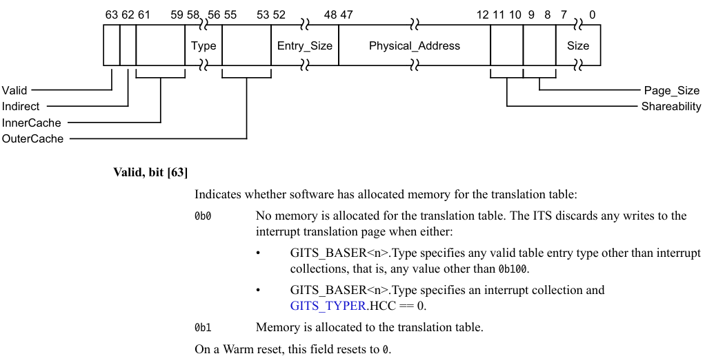
Image text
63 62 61 59 58 56 55 53 52 48 47 12 11 10 9 8 7 0
Type Entry_Size Physical_Address Size
Valid Page_Size
Indirect Shareability
InnerCache
OuterCache
Valid, bit [63]
Indicates whether software has allocated memory for the translation table:
0b0 No memory is allocated for the translation table. The ITS discards any writes to the
interrupt translation page when either:
• GITS_BASER
collections, that is, any value other than 0b100.
• GITS_BASER
GITS_TYPER.HCC == 0.
0b1 Memory is allocated to the translation table.
On a Warm reset, this field resets to 0.
0b0 Single Level. The Size field indicates the number of pages used by the ITS to store data associated with each table entry. 0b1 Two Level. The Size field indicates the number of pages which contain an array of 64-bit descriptors to pages that are used to store the data associated with each table entry. A little endian memory order model is used.
For more information, see The ITS tables.
This field is RAZ/WI for GIC implementations that only support flat tables. If the maximum width of the scaling factor that is identified by GITS_BASER
On a Warm reset, this field resets to an architecturally UNKNOWN value.
InnerCache, bits [61:59]
Indicates the Inner Cacheability attributes of accesses to the table. The possible values of this field are:
0b000 Device-nGnRnE. 0b001 Normal Inner Non-cacheable. 0b010 Normal Inner Cacheable Read-allocate, Write-through. 0b011 Normal Inner Cacheable Read-allocate, Write-back. 0b100 Normal Inner Cacheable Write-allocate, Write-through. 0b101 Normal Inner Cacheable Write-allocate, Write-back. 0b110 Normal Inner Cacheable Read-allocate, Write-allocate, Write-through. 0b111 Normal Inner Cacheable Read-allocate, Write-allocate, Write-back.
On a Warm reset, this field resets to an architecturally UNKNOWN value.
Type, bits [58:56]
Read only. Specifies the type of entity that requires entries in the corresponding translation table. The possible values of the field are:
0b000 Unimplemented. This register does not correspond to a translation table. 0b001 Devices. This register corresponds to a translation table that scales with the width of the DeviceID. Only a single GITS_BASER
Other values are reserved.
For FEAT_GICv4p1, the registers are allocated as follows:
-
GITS_BASER0.Type is 0b001 (Device).
-
• GITS_BASER1.Type is either 0b100 (Collection Table) or 0b000 (Unimplemented). • GITS_BASER2.Type is either 0b010 (vPE) or 0b000 (Unimplemented). • GITS_BASER
.Type, where ‘n’ is in the range 3 to 7, is 0b000 (Unimplemented).
For FEAT_GICv3, FEAT_GICv3p1, and FEAT_GICv4, Arm recommends that the GITS_BASER
Other allocations of Type values are deprecated.
On a Warm reset, this field resets to an architecturally UNKNOWN value.
OuterCache, bits [55:53]
Indicates the Outer Cacheability attributes of accesses to the table. The possible values of this field are:
0b000 Memory type defined in InnerCache field. For Normal memory, Outer Cacheability is the same as Inner Cacheability.
0b001 Normal Outer Non-cacheable. 0b010 Normal Outer Cacheable Read-allocate, Write-through. 0b011 Normal Outer Cacheable Read-allocate, Write-back. 0b100 Normal Outer Cacheable Write-allocate, Write-through. 0b101 Normal Outer Cacheable Write-allocate, Write-back. 0b110 Normal Outer Cacheable Read-allocate, Write-allocate, Write-through. 0b111 Normal Outer Cacheable Read-allocate, Write-allocate, Write-back.
It is IMPLEMENTATION DEFINED whether this field has a fixed value or can be programmed by software. Implementing this field with a fixed value is deprecated.
On a Warm reset, this field resets to an architecturally UNKNOWN value.
Entry_Size, bits [52:48]
Read-only. Specifies the number of bytes per translation table entry, minus one.
Physical_Address, bits [47:12]
Physical Address. When Page_Size is 4KB or 16KB:
-
Bits [51:48] of the base physical address are zero.
-
This field provides bits[47:12] of the base physical address of the table.
-
Bits[11:0] of the base physical address are zero.
-
The address must be aligned to the size specified in the Page Size field. Otherwise the effect is CONSTRAINED UNPREDICTABLE, and can be one of the following:
-
Bits[X:12], where X is derived from the page size, are treated as zero.
-
The value of bits[X:12] are used when calculating the address of a table access.
-
-
When Page_Size is 64KB:
-
Bits[47:16] of the register provide bits[47:16] of the base physical address of the table.
-
Bits[15:12] of the register provide bits[51:48] of the base physical address of the table.
-
Bits[15:0] of the base physical address are 0.
-
In implementations that support fewer than 52 bits of physical address, any unimplemented upper bits might be RAZ/WI.
On a Warm reset, this field resets to an architecturally UNKNOWN value.
Shareability, bits [11:10]
Indicates the Shareability attributes of accesses to the table. The possible values of this field are:
0b00 Non-shareable. 0b01 Inner Shareable. 0b10 Outer Shareable. 0b11 Reserved. Treated as 0b00.
It is IMPLEMENTATION DEFINED whether this field has a fixed value or can be programmed by software. Implementing this field with a fixed value is deprecated.
On a Warm reset, this field resets to an architecturally UNKNOWN value.
Page_Size, bits [9:8]
The size of page that the translation table uses:
0b00 4KB. 0b01 16KB. 0b10 64KB. 0b11 Reserved. Treated as 0b10.
Note If the GIC implementation supports only a single, fixed page size, this field might be RO.
On a Warm reset, this field resets to an architecturally UNKNOWN value.
Size, bits [7:0]
The number of pages of physical memory allocated to the table, minus one. GITS_BASER
If GITS_BASER
On a Warm reset, this field resets to an architecturally UNKNOWN value.
Accessing the GITS_BASER:
GITS_BASER
| Component | Offset | Instance |
|---|---|---|
| GIC ITS control | 0x0100+ (8 * n) | GITS_BASER |
This interface is accessible as follows:
-
When GICD_CTLR.DS == 0 accesses to this register are RW.
-
When an access is Secure accesses to this register are RW.
-
When an access is Non-secure accesses to this register are RW.
12.19.2 GITS_CBASER, ITS Command Queue Descriptor
The GITS_CBASER characteristics are:
Purpose
Specifies the base address and size of the ITS command queue.
Configurations
Bits [63:32] and bits [31:0] are accessible separately.
Attributes
GITS_CBASER is a 64-bit register.
Field descriptions
The GITS_CBASER bit assignments are:
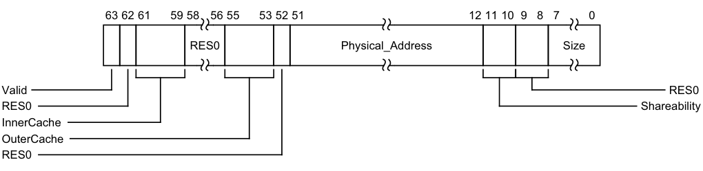
Image text
63 62 61 59 58 56 55 53 52 51 12 11 10 9 8 7 0
RES0 Physical_Address Size
Valid RES0
RES0 Shareability
InnerCache
OuterCache
RES0
Bit [62]
Reserved, RES0.
InnerCache, bits [61:59]
Indicates the Inner Cacheability attributes of accesses to the command queue. The possible values of this field are:
0b000 Device-nGnRnE. 0b001 Normal Inner Non-cacheable. 0b010 Normal Inner Cacheable Read-allocate, Write-through. 0b011 Normal Inner Cacheable Read-allocate, Write-back. 0b100 Normal Inner Cacheable Write-allocate, Write-through. 0b101 Normal Inner Cacheable Write-allocate, Write-back. 0b110 Normal Inner Cacheable Read-allocate, Write-allocate, Write-through. 0b111 Normal Inner Cacheable Read-allocate, Write-allocate, Write-back. On a Warm reset, this field resets to an architecturally UNKNOWN value.
Bits [58:56]
Reserved, RES0.
OuterCache, bits [55:53]
Indicates the Outer Cacheability attributes of accesses to the command queue. The possible values of this field are:
0b000 Memory type defined in InnerCache field. For Normal memory, Outer Cacheability is the same as Inner Cacheability. 0b001 Normal Outer Non-cacheable. 0b010 Normal Outer Cacheable Read-allocate, Write-through. 0b011 Normal Outer Cacheable Read-allocate, Write-back. 0b100 Normal Outer Cacheable Write-allocate, Write-through. 0b101 Normal Outer Cacheable Write-allocate, Write-back. 0b110 Normal Outer Cacheable Read-allocate, Write-allocate, Write-through. 0b111 Normal Outer Cacheable Read-allocate, Write-allocate, Write-back.
It is IMPLEMENTATION DEFINED whether this field has a fixed value or can be programmed by software. Implementing this field with a fixed value is deprecated.
On a Warm reset, this field resets to an architecturally UNKNOWN value.
Bit [52]
Reserved, RES0.
Physical_Address, bits [51:12]
- Bits [51:12] of the base physical address of the command queue. Bits [11:0] of the base address are 0.
In implementations supporting fewer than 52 bits of physical address, unimplemented upper bits are RES0.
If bits [15:12] are not all zeros, behavior is a CONSTRAINED UNPREDICTABLE choice:
-
Bits [15:12] are treated as if all the bits are zero. The value read back from those bits is either the value written or zero.
-
The result of the calculation of an address for a command queue read can be corrupted.
-
On a Warm reset, this field resets to an architecturally UNKNOWN value.
Shareability, bits [11:10]
Indicates the Shareability attributes of accesses to the command queue. The possible values of this field are:
0b00 Non-shareable. 0b01 Inner Shareable. 0b10 Outer Shareable. 0b11 Reserved. Treated as 0b00.
It is IMPLEMENTATION DEFINED whether this field has a fixed value or can be programmed by software. Implementing this field with a fixed value is deprecated.
On a Warm reset, this field resets to an architecturally UNKNOWN value.
Bits [9:8]
Reserved, RES0.
Size, bits [7:0]
The number of 4KB pages of physical memory allocated to the command queue, minus one.
On a Warm reset, this field resets to an architecturally UNKNOWN value.
The command queue is a circular buffer and wraps at Physical Address [47:0] + (4096 * (Size + 1)).
Note When this register is successfully written, the value of GITS_CREADR is set to zero.
Accessing the GITS_CBASER:
When GITS_CTLR.Enabled == 1 or GITS_CTLR.Quiescent == 0, writing this register is UNPREDICTABLE.
GITS_CBASER can be accessed through its memory-mapped interface:
Component Offset Instance GIC ITS control 0x0080 GITS_CBASER
This interface is accessible as follows:
-
When GICD_CTLR.DS == 0 accesses to this register are RW.
-
When an access is Secure accesses to this register are RW.
-
When an access is Non-secure accesses to this register are RW.
12.19.3 GITS_CREADR, ITS Read Register
The GITS_CREADR characteristics are:
Purpose
Specifies the offset from GITS_CBASER where the ITS reads the next ITS command.
Configurations
This register is cleared to 0 when a value is written to GITS_CBASER. Bits [63:32] and bits [31:0] are accessible separately.
Attributes
GITS_CREADR is a 64-bit register.
Field descriptions
The GITS_CREADR bit assignments are:

63 20 19 5 4 1 0
RES0 Offset RES0
Stalled
Bits [63:20]
Reserved, RES0.
Offset, bits [19:5]
Bits [19:5] of the offset from GITS_CBASER. Bits [4:0] of the offset are zero.
Bits [4:1]
Reserved, RES0.
Stalled, bit [0]
Reports whether the processing of commands is stalled because of a command error. 0b0 ITS command queue is not stalled because of a command error. 0b1 ITS command queue is stalled because of a command error.
For more information, see The ITS command interface.
Accessing the GITS_CREADR:
GITS_CREADR can be accessed through its memory-mapped interface:
Component Offset Instance GIC ITS control 0x0090 GITS_CREADR
This interface is accessible as follows:
-
When GICD_CTLR.DS == 0 accesses to this register are RO.
-
When an access is Secure accesses to this register are RO.
-
When an access is Non-secure accesses to this register are RO.
12.19.4 GITS_CTLR, ITS Control Register
The GITS_CTLR characteristics are:
Purpose
Controls the operation of an ITS.
Configurations
The ITS_Number (bits [7:4]) and bit [1] fields apply only in FEAT_GICv4 implementations, and are RES0 in FEAT_GICv3 implementations.
Attributes
GITS_CTLR is a 32-bit register.
Field descriptions
The GITS_CTLR bit assignments are:
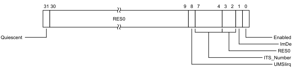
Image text
31 30 9 8 7 4 3 2 1 0
RES0
Quiescent Enabled
ImDe
RES0
ITS_Number
UMSIirq
-
0b0 The ITS is not quiescent and cannot be powered down.
-
0b1 The ITS is quiescent and can be powered down.
For the ITS to be considered inactive, there must be no transactions in progress. In addition, all operations required to ensure that mapping data is consistent with external memory must be complete.
Note In distributed GIC implementations, this bit is set to 1 only after the ITS forwards any operations that have not yet been completed to the Redistributors and receives confirmation that all such operations have reached the appropriate Redistributor.
In FEAT_GICv3, FEAT_GICv3p1, and FEAT_GICv4, when GITS_CTLR.Enabled == 1, the value of GITS_CTLR.Quiescent is UNKNOWN.
In FEAT_GICv4p1, when GITS_CTLR.Enabled == 1, the value of GITS_CTLR.Quiescent reads as 1 until the write to Enabled has taken effect and then reads as 0.
On a Warm reset, this field resets to 1.
Bits [30:9]
Reserved, RES0.
UMSIirq, bit [8]
Unmapped MSI reporting interrupt enable.
- 0b0 The ITS does not assert an interrupt signal when GITS_STATUSR.UMSI is 1. 0b1 The ITS asserts an interrupt signal when GITS_STATUSR.UMSI is 1. If GITS_TYPER.UMSIirq is 0, this field is RES0.
On a Warm reset, this field resets to 0.
ITS_Number, bits [7:4]
In FEAT_GICv3 implementations this field is RES0.
In FEAT_GICv4 implementations with more than one ITS instance, this field indicates the ITS number for use with VMOVP GICv4.0.
It is IMPLEMENTATION DEFINED whether this field is programmable or RO.
If this field is programmable, changing this field when GITS_CTLR.Quiescent == 0 or GITS_CTLR.Enabled == 1 is UNPREDICTABLE.
On a Warm reset, this field resets to an architecturally UNKNOWN value.
Bits [3:2]
Reserved, RES0.
ImDe, bit [1]
In GICv3 implementations, this bit is RES0.
In GICv4 implementations, this bit is IMPLEMENTATION DEFINED.
On a Warm reset, this field resets to 0.
Enabled, bit [0]
Controls whether the ITS is enabled:
0b0 The ITS is not enabled. Writes to GITS_TRANSLATER are ignored and no further command queue entries are processed.
0b1 The ITS is enabled. Writes to GITS_TRANSLATER result in interrupt translations and the command queue is processed.
If a write to this register changes this field from 1 to 0, the ITS must ensure that both:
-
Any caches containing mapping data are made consistent with external memory.
-
GITS_CTLR.Quiescent == 0 until all caches are consistent with external memory.
Changing GITS_CTLR.Enabled from 0 to 1 when GITS_CTLR.Quiescent is 0 results in UNPREDICTABLE behavior.
On a Warm reset, this field resets to 0.
Accessing the GITS_CTLR:
GITS_CTLR can be accessed through its memory-mapped interface:
Component Offset Instance GIC ITS control 0x0000 GITS_CTLR
This interface is accessible as follows:
-
When GICD_CTLR.DS == 0 accesses to this register are RW.
-
When an access is Secure accesses to this register are RW.
-
When an access is Non-secure accesses to this register are RW.
12.19.5 GITS_CWRITER, ITS Write Register
The GITS_CWRITER characteristics are:
Purpose
Specifies the offset from GITS_CBASER where software writes the next ITS command.
Configurations
Bits [63:32] and bits [31:0] are accessible separately.
Attributes
GITS_CWRITER is a 64-bit register.
Field descriptions
The GITS_CWRITER bit assignments are:

63 20 19 5 4 1 0
RES0 Offset RES0
Retry
Bits [63:20]
Reserved, RES0.
Offset, bits [19:5]
Bits [19:5] of the offset from GITS_CBASER. Bits [4:0] of the offset are zero.
On a Warm reset, this field resets to an architecturally UNKNOWN value.
Bits [4:1]
Reserved, RES0.
Retry, bit [0]
Writing this bit has the following effects:
0b0 No effect on the processing commands by the ITS. 0b1 Restarts the processing of commands by the ITS if it stalled because of a command error.
Note If the processing of commands is not stalled because of a command error, writing 1 to this bit has no effect.
When read, this bit is RES0.
For more information, see The ITS command interface.
If GITS_CWRITER is written with a value outside of the valid range specified by
GITS_CBASER.Physical_Address and GITS_CBASER.Size, behavior is a CONSTRAINED UNPREDICTABLE choice, as follows:
-
The command queue is considered invalid, and no further commands are processed until GITS_CWRITER is written with a value that is in the valid range.
-
The value is treated as a valid UNKNOWN value.
An implementation might choose to report a system error in an IMPLEMENTATION DEFINED manner.
Accessing the GITS_CWRITER:
GITS_CWRITER can be accessed through its memory-mapped interface:
| Component | Offset | Instance |
|---|---|---|
| GIC ITS control | 0x0088 | GITS_CWRITER |
This interface is accessible as follows:
-
When GICD_CTLR.DS == 0 accesses to this register are RW.
-
When an access is Secure accesses to this register are RW.
-
When an access is Non-secure accesses to this register are RW.
12.19.6 GITS_IIDR, ITS Identification Register
The GITS_IIDR characteristics are:
Purpose
Provides information about the implementer and revision of the ITS.
Configurations
This register is available in all configurations of the GIC. If the GIC implementation supports two Security states, this register is Common.
Attributes
GITS_IIDR is a 32-bit register.
Field descriptions
The GITS_IIDR bit assignments are:
| | 31 | | 24 | 23 | | 20 | 19 | | 16 | 15 | | 12 | 11 | | 0 | | |—|—|— ProductID |—|—|— RES0 |—|—|— Variant |—|—|— Revision |—|—|— Implementer |—|—| ||||||||||||||||||
ProductID, bits [31:24]
An IMPLEMENTATION DEFINED product identifier.
Bits [23:20]
Reserved, RES0.
Variant, bits [19:16]
An IMPLEMENTATION DEFINED variant number. Typically, this field is used to distinguish product variants, or major revisions of a product.
Revision, bits [15:12]
An IMPLEMENTATION DEFINED revision number. Typically, this field is used to distinguish minor revisions of a product.
Implementer, bits [11:0]
Contains the JEP106 code of the company that implemented the ITS:
-
Bits [11:8] are the JEP106 continuation code of the implementer. For an Arm implementation, this field is 0x4.
-
Bit [7] is always 0.
-
Bits [6:0] are the JEP106 identity code of the implementer. For an Arm implementation, bits [7:0] are therefore 0x3B.
Accessing the GITS_IIDR:
GITS_IIDR can be accessed through its memory-mapped interface:
Component Offset Instance GIC ITS control 0x0004 GITS_IIDR This interface is accessible as follows:
-
When GICD_CTLR.DS == 0 accesses to this register are RO.
-
When an access is Secure accesses to this register are RO.
-
When an access is Non-secure accesses to this register are RO.
12.19.7 GITS_MPAMIDR, Report maximum PARTID and PMG Register
The GITS_MPAMIDR characteristics are:
Purpose
Reports the maximum support PARTID and PMG values.
Configurations
This register is present only when FEAT_GICv3p1 is implemented. Otherwise, direct accesses to GITS_MPAMIDR are RES0.
A copy of this register is provided for each ITS.
When GITS_TYPER.MPAM==0, this register is RES0.
Attributes
GITS_MPAMIDR is a 32-bit register.
Field descriptions
The GITS_MPAMIDR bit assignments are:

31 24 23 16 15 0
RES0 PMGmax PARTIDmax
Bits [31:24]
Reserved, RES0.
PMGmax, bits [23:16]
Maximum PMG value supported.
PARTIDmax, bits [15:0]
Maximum PARTID value supported.
Accessing the GITS_MPAMIDR:
GITS_MPAMIDR can be accessed through its memory-mapped interface:
Component Offset
GIC ITS control 0x0010
This interface is accessible as follows:
-
When GICD_CTLR.DS == 0 accesses to this register are RO.
-
When an access is Secure accesses to this register are RO.
-
When an access is Non-secure accesses to this register are RO.
12.19.8 GITS_MPIDR, Report ITS’s affinity.
The GITS_MPIDR characteristics are:
Purpose
Reports ITS’s affinity when the vPE Table is shared with Redistributors.
Configurations
This register is present only when FEAT_GICv4p1 is implemented. Otherwise, direct accesses to GITS_MPIDR are RES0.
A copy of this register is provided for each ITS.
When GITS_TYPER.SVPET==0, this register is RES0.
Attributes
GITS_MPIDR is a 32-bit register.
Field descriptions
The GITS_MPIDR bit assignments are:
| | 31 | | 24 | 23 | | 16 | 15 | | 8 | 7 | | 0 | | |—|—|— Aff3 |—|—|— Aff2 |—|—|— Aff1 |—|—|— RES0 |—|—| |||||||||||||||
Aff3, bits [31:24]
The Affinity level 3 value for the ITS.
Aff2, bits [23:16]
The Affinity level 2 value for the ITS.
Aff1, bits [15:8]
The Affinity level 1 value for the ITS.
Bits [7:0]
Reserved, RES0.
Accessing the GITS_MPIDR:
GITS_MPIDR can be accessed through its memory-mapped interface:
Component Offset
GIC ITS control 0x0018
This interface is accessible as follows:
-
When GICD_CTLR.DS == 0 accesses to this register are RO.
-
When an access is Secure accesses to this register are RO.
-
When an access is Non-secure accesses to this register are RO.
12.19.9 GITS_PARTIDR, Set PARTID and PMG Register
The GITS_PARTIDR characteristics are:
Purpose
Sets the PARTID and PMG values used for memory accesses by the ITS.
Configurations
This register is present only when FEAT_GICv3p1 is implemented. Otherwise, direct accesses to GITS_PARTIDR are RES0.
A copy of this register is provided for each ITS.
When GITS_TYPER.MPAM==0, this register is RES0.
Attributes
GITS_PARTIDR is a 32-bit register.
Field descriptions
The GITS_PARTIDR bit assignments are:

31 24 23 16 15 0
RES0 PMG PARTID
Bits [31:24]
Reserved, RES0.
PMG, bits [23:16]
PMG value used when ITS accesses memory.
It is IMPLEMENTATION DEFINED whether bits not needed to represent PMG values in the range 0 to PMG_MAX are stateful or RES0.
On a Warm reset, this field resets to 0.
PARTID, bits [15:0]
PARTID value used when ITS accesses memory.
It is IMPLEMENTATION DEFINED whether bits not needed to represent PARTID values in the range 0 to PARTID_MAX are stateful or RES0.
On a Warm reset, this field resets to 0.
Accessing the GITS_PARTIDR:
GITS_PARTIDR can be accessed through its memory-mapped interface:
Component Offset
GIC ITS control 0x0014
This interface is accessible as follows:
-
When GICD_CTLR.DS == 0 accesses to this register are RW.
-
When an access is Secure accesses to this register are RW.
-
When an access is Non-secure accesses to this register are RW.
12.19.10 GITS_SGIR, ITS SGI Register
The GITS_SGIR characteristics are:
Purpose
Written by software to signal a virtual SGI for translation by the ITS.
Configurations
This register is present only when FEAT_GICv4p1 is implemented. Otherwise, direct accesses to GITS_SGIR are RES0.
This register is provided only in FEAT_GICv4p1 implementations.
Attributes
GITS_SGIR is a 64-bit register.
Field descriptions
The GITS_SGIR bit assignments are:
| | 63 | | 48 | 47 | | 32 | 31 | | 4 | 3 | 0 | | |—|—|— RES0 |—|—|— vPEID |—|—|— RES0 |—|— vINTID |—|—| ||||||||||||||
Bits [63:48]
Reserved, RES0.
vPEID, bits [47:32]
ID of target vPEID.
The size of this field is IMPLEMENTATION DEFINED, and is specified by the GICD_TYPER2.VIL and GICD_TYPER2.VID fields. Unimplemented bits are RES0.
Bits [31:4]
Reserved, RES0.
vINTID, bits [3:0]
INTID of virtual SGI.
Accessing the GITS_SGIR:
64-bit access only.
GITS_SGIR can be accessed through its memory-mapped interface:
Component Offset
GIC ITS control 0x20020
This interface is accessible as follows:
-
When GICD_CTLR.DS == 0 accesses to this register are WO.
-
When an access is Secure accesses to this register are WO.
-
When an access is Non-secure accesses to this register are WO.
12.19.11 GITS_STATUSR, ITS Error Reporting Status Register
The GITS_STATUSR characteristics are:
Purpose
Provides software with a mechanism to detect:
-
Accesses to reserved locations.
-
• Writes to read-only locations. • Reads of write-only locations.
-
Unmapped MSIs.
Configurations
There are no configuration notes.
Attributes
GITS_STATUSR is a 32-bit register.
Field descriptions
The GITS_STATUSR bit assignments are:
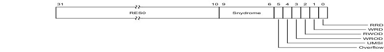
Image text
31 10 9 6 5 4 3 2 1 0
RES0 Snydrome
RRD
WRD
RWOD
WROD
UMSI
Overflow
Snydrome, bits [9:6]
Syndrome for the MSI that set GITS_STATUSR.UMSI to 1.
0b0000 Unknown reason. 0b0010 DeviceID out of range. 0b0011 DeviceID unmapped. 0b0100 EventID out of range. 0b0101 EventID unmapped. 0b0111 Collection unmapped. 0b1001 vPEID unmapped.
An implementation might not support reporting all syndromes, and might report 0b0000 for any cause.
This field is UNKNOWN when GITS_STATUSR.UMSI is 0.
Overflow, bit [5]
Reports whether an unmapped MSI has been received while GITS_STATUSR.UMSI is 1.
- 0b0 No unmapped MSIs have been received since GITS_STATUSR.UMSI set to 1. 0b1 At least one unmapped MSIs have been received since GITS_STATUSR.UMSI set to 1.
A software write of 1 to the bit clears it. A write of any other value is ignored.
If GITS_TYPER.UMSI is 0, this field is RES0.
UMSI, bit [4]
Reports whether an unmapped MSI has been received 0b0 No unmapped MSIs have been received. 0b1 Unampped MSI received. A software write of 1 to the bit clears it. A write of any other value is ignored. If GITS_TYPER.UMSI is 0, this field is RES0.
WROD, bit [3]
Write to an RO location. 0b0 Normal operation. 0b1 A write to an RO location has been detected. When a violation is detected, software must write 1 to this register to reset it.
RWOD, bit [2]
Read of a WO location. 0b0 Normal operation. 0b1 A read of a WO location has been detected. When a violation is detected, software must write 1 to this register to reset it.
WRD, bit [1]
Write to a reserved location. 0b0 Normal operation. 0b1 A write to a reserved location has been detected. When a violation is detected, software must write 1 to this register to reset it.
RRD, bit [0]
Read of a reserved location. 0b0 Normal operation. 0b1 A read of a reserved location has been detected. When a violation is detected, software must write 1 to this register to reset it.
Accessing the GITS_STATUSR:
This is an optional register. If the register is not implemented, the location is RAZ/WI.
GITS_STATUSR can be accessed through its memory-mapped interface:
Component Offset Instance GIC ITS control 0x0040 GITS_STATUSR
This interface is accessible as follows:
-
When GICD_CTLR.DS == 0 accesses to this register are RO.
-
When an access is Secure accesses to this register are RW.
-
When an access is Non-secure accesses to this register are RW.
12.19.12 GITS_TRANSLATER, ITS Translation Register
The GITS_TRANSLATER characteristics are:
Purpose
Written by a requesting Device to signal an interrupt for translation by the ITS.
Configurations
This register is at the same offset as GICD_SETSPI_NSR in the Distributor, and is at the same offset as GICR_SETLPIR in the Redistributor.
Attributes
GITS_TRANSLATER is a 32-bit register.
Field descriptions
The GITS_TRANSLATER bit assignments are:

31 0
EventID
EventID, bits [31:0]
An identifier corresponding to the interrupt to be translated.
Note
The size of the EventID is DeviceID specific, and set when the DeviceID is mapped to an ITT (using MAPD).
The number of EventID bits implemented is reported by GITS_TYPER.ID_bits. If a write specifies non-zero identifiers bits outside this range behavior is a CONSTRAINED UNPREDICTABLE choice between:
-
Non-zero identifier bits outside the supported range are ignored.
-
The write is ignored.
The DeviceID presented to an ITS is used to index a device table. The device table maps the DeviceID to an interrupt translation table for that device.
Accessing the GITS_TRANSLATER:
16-bit access to bits [15:0] of this register must be supported. When this register is written by a 16-bit transaction, bits [31:16] are written as zero.
Implementations must ensure that:
-
A unique DeviceID is provided for each requesting device, and the DeviceID is presented to the ITS when a write to this register occurs in a manner that cannot be spoofed by any agent capable of performing writes.
-
The DeviceID presented corresponds to the DeviceID field in the ITS commands.
Writes to this register are ignored if any of the following are true:
-
GITS_CTLR.Enabled == 0.
-
The presented DeviceID is not mapped to an Interrupt Translation Table.
-
The DeviceID is larger than the supported size.
-
The DeviceID is mapped to an Interrupt Translation Table, but the EventID is outside the range specified by MAPD.
-
The EventID is mapped to an Interrupt Translation Table and the EventID is within the range specified by MAPD, but the EventID is unmapped.
Translation requests that result from writes to this register are subject to certain ordering rules. For more information, see Ordering of translations with the output to ITS commands.
GITS_TRANSLATER can be accessed through its memory-mapped interface:
| Component | Offset | Instance |
|---|---|---|
| GIC ITS translation | 0x0040 | GITS_TRANSLATER |
This interface is accessible as follows:
-
When GICD_CTLR.DS == 0 accesses to this register are WO.
-
When an access is Secure accesses to this register are WO.
-
When an access is Non-secure accesses to this register are WO.
12.19.13 GITS_TYPER, ITS Type Register
The GITS_TYPER characteristics are:
Purpose
Specifies the features that an ITS supports.
Configurations
There are no configuration notes.
Attributes
GITS_TYPER is a 64-bit register.
Field descriptions
The GITS_TYPER bit assignments are:
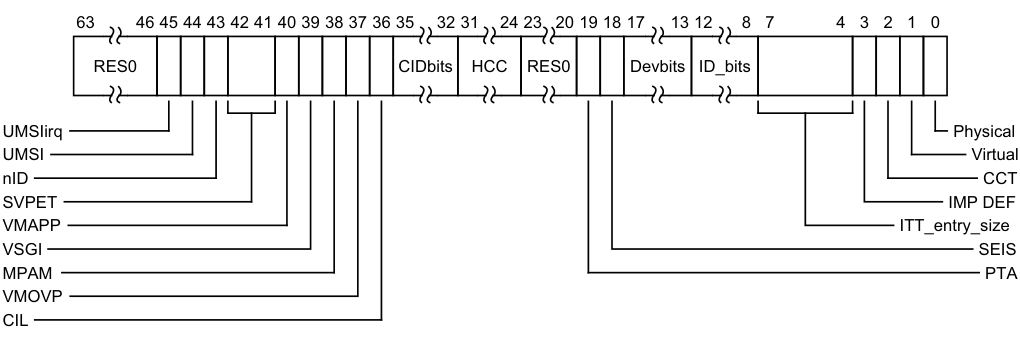
Image text
63 46 45 44 43 42 41 40 39 38 37 36 35 32 31 24 23 20 19 18 17 13 12 8 7 4 3 2 1 0
RES0 CIDbits HCC RES0 Devbits ID_bits
UMSIirq Physical
UMSI Virtual
nID CCT
SVPET IMP DEF
VMAPP ITT_entry_size
VSGI SEIS
MPAM PTA
VMOVP
CIL
Reserved, RES0. Indicates support for generating an interrupt on receiving unmapped MSI. 0b0 Interrupt on unmapped MSI not supported. 0b1 Interrupt on unmapped MSI is supported. If GITS_TYPER.UMSI is 0, this field is RES0. Indicates suport for reporting receipt of unmapped MSIs. 0b0 Reporting of unmapped MSIs is not supported. 0b1 Reporting of unmapped MSIs is supported. When FEAT_GICv4p1 is implemented: nID nID 0b0 Individual doorbell interrupt supported. 0b1 Individual doorbell interrupt not supported.
UMSIirq, bit [45]
UMSI, bit [44]
nID, bit [43]
Otherwise:
Reserved, RES0.
When FEAT_GICv4p1 is implemented:
nID nID 0b0 Individual doorbell interrupt supported. 0b1 Individual doorbell interrupt not supported.
Otherwise:
Reserved, RES0.
SVPET, bits [42:41]
When FEAT_GICv4p1 is implemented:
SVPET SVPET 0b00 vPE Table is not shared with Redistributors. 0b01 vPE Table is shared with the groups of Redistributors indicated by GITS_MPIDR.Aff3. 0b10 vPE Table is shared with the groups of Redistributors indicated by GITS_MPIDR fields Aff3 and Aff2. 0b11 vPE Table is shared with the groups of Redistributors indicated by GITS_MPIDR fields Aff3, Aff2 and Aff1.
Otherwise:
Reserved, RES0.
VMAPP, bit [40]
When FEAT_GICv4p1 is implemented:
VMAPP VMAPP 0b0 FEAT_GICv4 VMAPP command layout. 0b1 FEAT_GICv4p1 VMAPP command layout.
Otherwise:
Reserved, RES0.
When FEAT_GICv4p1 is implemented:
VMAPP VMAPP 0b0 FEAT_GICv4 VMAPP command layout. 0b1 FEAT_GICv4p1 VMAPP command layout.
Otherwise:
Reserved, RES0.
VSGI, bit [39]
When FEAT_GICv4p1 is implemented:
VSGI VSGI 0b0 Direct injection of SGIs is not supported. 0b1 Direct injection of SGIs is supported.
Otherwise:
Reserved, RES0.
When FEAT_GICv4p1 is implemented:
VSGI VSGI 0b0 Direct injection of SGIs is not supported. 0b1 Direct injection of SGIs is supported.
Otherwise:
Reserved, RES0.
MPAM, bit [38]
When FEAT_GICv3p1 is implemented:
MPAM MPAM 0b0 MPAM is not supported. 0b1 MPAM is supported. Otherwise: Reserved, RES0. When FEAT_GICv3p1 is implemented: MPAM MPAM 0b0 MPAM is not supported. 0b1 MPAM is supported.
Otherwise:
Reserved, RES0.
VMOVP, bit [37]
Indicates the form of the VMOVP command.
0b0 When moving a vPE, software must issue a VMOVP on all ITSs that have mappings for that vPE. The ITSList and Sequence Number fields in the VMOVP command must ensure synchronization, otherwise behavior is UNPREDICTABLE. 0b1 When moving a vPE, software must only issue a VMOVP on one of the ITSs that has a mapping for that vPE. The ITSList and Sequence Number fields in the VMOVP command are RES0.
CIL, bit [36]
Collection ID Limit.
0b0 ITS supports 16-bit Collection ID, GITS_TYPER.CIDbits is RES0. 0b1 GITS_TYPER.CIDbits indicates supported Collection ID size
In implementations that do not support Collections in external memory, this bit is RES0 and the number of Collections supported is reported by GITS_TYPER.HCC.
CIDbits, bits [35:32]
Number of Collection ID bits.
-
The number of bits of Collection ID minus one.
-
When GITS_TYPER.CIL == 0, this field is RES0.
HCC, bits [31:24]
Hardware Collection Count. The number of interrupt collections supported by the ITS without provisioning of external memory.
Note
Collections held in hardware are unmapped at reset.
Bits [23:20]
Reserved, RES0.
PTA, bit [19]
Physical Target Addresses. Indicates the format of the target address:
SEIS, bit [18]
0b0 The target address corresponds to the PE number specified by GICR_TYPER.Processor_Number. 0b1 The target address corresponds to the base physical address of the required Redistributor. For more information, see RDbase. SEI support. Indicates whether the virtual CPU interface supports generation of SEIs: 0b0 The ITS does not support local generation of SEIs. 0b1 The ITS supports local generation of SEIs.
Devbits, bits [17:13]
The number of DeviceID bits implemented, minus one.
ID_bits, bits [12:8]
The number of EventID bits implemented, minus one.
ITT_entry_size, bits [7:4]
Read-only. Indicates the number of bytes per translation table entry, minus one.
For more information about the ITS command ‘MAPD’, see MAPD.
IMPLEMENTATION DEFINED, bit [3]
IMPLEMENTATION DEFINED.
CCT, bit [2]
Cumulative Collection Tables.
0b0 The total number of supported collections is determined by the number of collections held in memory only.
0b1 The total number of supported collections is determined by number of collections that are held in memory and the number indicated by GITS_TYPER.HCC.
If GITS_TYPER.HCC == 0, or if memory backed collections are not supported (all GITS_BASER
Virtual, bit [1]
When FEAT_GICv4 is implemented:
Virtual
Indicates whether the ITS supports virtual LPIs and direct injection of virtual LPIs:
0b0 The ITS does not support virtual LPIs or direct injection of virtual LPIs. 0b1 The ITS supports virtual LPIs and direct injection of virtual LPIs.
Otherwise:
Reserved, RES0.
When FEAT_GICv4 is implemented:
Virtual
Indicates whether the ITS supports virtual LPIs and direct injection of virtual LPIs: 0b0 The ITS does not support virtual LPIs or direct injection of virtual LPIs. 0b1 The ITS supports virtual LPIs and direct injection of virtual LPIs.
Otherwise:
Reserved, RES0.
Physical, bit [0]
Indicates whether the ITS supports physical LPIs: 0b0 The ITS does not support physical LPIs. 0b1 The ITS supports physical LPIs.
This field is RES1, indicating that the ITS supports physical LPIs.
Accessing the GITS_TYPER:
GITS_TYPER can be accessed through its memory-mapped interface:
| Component | Offset | Instance |
|---|---|---|
| GIC ITS control | 0x0008 | GITS_TYPER |
This interface is accessible as follows:
-
When GICD_CTLR.DS == 0 accesses to this register are RO.
-
When an access is Secure accesses to this register are RO.
-
When an access is Non-secure accesses to this register are RO.
12.19.14 GITS_UMSIR, ITS Unmapped MSI register
The GITS_UMSIR characteristics are:
Purpose
Provides the DeviceID and EventID of the unmapped MSI that set GITS_STATUSR.UMSI.
Configurations
This register is present only when GITS_TYPER.UMSI == 1. Otherwise, direct accesses to GITS_UMSIR are RES0.
Attributes
GITS_UMSIR is a 64-bit register.
Field descriptions
The GITS_UMSIR bit assignments are:

63 32 31 0
DeviceID EventID
DeviceID, bits [63:32]
DeviceID of MSI that set GITS_STATUSR.UMSI to 1.
If GITS_STATUSR.UMSI is 0, this field is UNKNOWN.
EventID, bits [31:0]
EventID of MSI that set GITS_STATUSR.UMSI to 1.
If GITS_STATUSR.UMSI is 0, this field is UNKNOWN.
Accessing the GITS_UMSIR:
GITS_UMSIR can be accessed through its memory-mapped interface:
Component Offset Instance GIC ITS control 0x0048 GITS_UMSIR
This interface is accessible as follows:
-
When GICD_CTLR.DS == 0 accesses to this register are RO.
-
When an access is Secure accesses to this register are RW.
-
When an access is Non-secure accesses to this register are RW.
12.20 Pseudocode
AArch64 functions shows the pseudocode for the System registers when executing in AArch64 state. The same pseudocode can be used for the System registers when executing in AArch32 state by substituting the AArch64 register names with the equivalent AArch32 register names.
Note An AArch64 register name includes the lowest Exception level that can access the register as a suffix to the register name. An AArch32 register name does not contain this suffix. For example the AArch64 Interrupt Controller Deactivate Interrupt Register is ICC_DIR_EL1, while the AArch32 equivalent is ICC_DIR.
Functions for memory-mapped registers shows the pseudocode for the memory-mapped registers.
Note
Some variable names used the pseudocode differ from those used in the body text. For a list of the affected variables, see _Pseudocode terminology_B-910.
12.20.1 AArch64 functions
This subsection describes the AArch64 functions. The functions are indicated by the hierarchical path names, for example aarch64/support. The functions are:
-
aarch64/support/ICC_DIR_EL1 .
-
aarch64/support/ICC_EOIR0_EL1.
-
aarch64/support/ICC_EOIR1_EL1.
-
aarch64/support/ICC_HPPIR0_EL1.
-
aarch64/support/ICC_HPPIR1_EL1.
-
aarch64/support/ICC_IAR0_EL1.
-
aarch64/support/ICC_IAR1_EL1.
-
aarch64/support/ICC_PMR_EL1.
-
aarch64/support/ICC_RPR_EL1.
-
aarch64/support/ICH_EISR_EL2.
-
aarch64/support/ICH_ELRSR_EL2.
-
aarch64/support/VirtualReadHPPIR0.
-
aarch64/support/VirtualReadHPPIR1.
-
aarch64/support/VirtualReadIAR0.
-
aarch64/support/VirtualReadIAR1.
-
aarch64/support/VirtualWriteDIR.
-
aarch64/support/VirtualWriteEOIR0.
-
aarch64/support/VirtualWriteEOIR1.
-
aarch64/support/CheckGroup0ForSpecialIdentifiers.
-
aarch64/support/CheckGroup1ForSpecialIdentifiers.
-
aarch64/support/PRIMask.
-
aarch64/support/VRIMask.
aarch64/support/ICC_DIR_EL1
// ICC_DIR_EL1 - assignment form // =============================
ICC_DIR_EL1[] = bits(64) data
// First check if System Registers are enabled SystemRegisterAccessPermitted(2, TRUE);
// Now check for special identifiers
if IsSpecial(intID) then
return FALSE; // It is a special ID
// All the checks pass so the identifier is valid
return TRUE;
aarch64/support/ICC_EOIR0_EL1
// ICC_EOIR0_EL1 - assignment form
// =============================== ICC_EOIR0_EL1[] =
bits(64) data eoiID = data<INTID_SIZE-1:0>;
// First check
if System Registers are enabled SystemRegisterAccessPermitted(0, FALSE);
// Check
if the access is virtual
if HaveEL(EL2) && EL2Enabled() && PSTATE.EL == EL1 && HCR_EL2.FMO == '1' then VirtualWriteEOIR0(data);
// Access the Virtual EOIR0 register return;
// Check
for spurious ID. LPIs are allowed and the access is physical
if !InterruptIdentifierValid(data, TRUE) then return;
// Now start handling the interrupt
// Is the highest priority G0S, G1S or G1NS pGroup = GetHighestActiveGroup(ICC_AP0R_EL1, ICC_AP1R_EL1NS, ICC_AP1R_EL1S);
pPriority = GetHighestActivePriority(ICC_AP0R_EL1, ICC_AP1R_EL1NS, ICC_AP1R_EL1S);
// If a device is Re-mapped software must perform the following actions
// to ensure the LPI configuration is up to date:
// 1. Ensure that the device is quiescent and that all interrupts have
// been handled.
// 2. Remap the device with the new (empty) ITT
//
DeviceTableEntry dte;
aarch64/support/ICC_EOIR1_EL1
// Check whether Non-secure EL1 is using system registers or not
if HaveEL(EL2) && (HCR_EL2.FMO == '1' || HCR_EL2.IMO == '1' || HCR_EL2.AMO == '1') then
// EL2 is implemented and at least one interrupt exception is virtualized
sreEL1NS = ((sreEL2 && ICC_SRE_EL1NS.SRE == '1') ||
(sreEL1S && (HCR_EL2.FMO == '0' || HCR_EL2.IMO == '0' || HCR_EL2.AMO == '0')));
elsif HaveEL(EL2) then
sreEL1NS = (ICC_SRE_EL2.SRE == '1' && ICC_SRE_EL1NS.SRE == '1') || sreEL1S;
else
sreEL1NS = ICC_SRE_EL1NS.SRE == '1' || sreEL1S;
// Check if System Registers are enabled for the EL and security state
if ((PSTATE.EL == EL2 && !IsSecure() && !sreEL2) ||
(PSTATE.EL == EL1 && IsSecure() && ICC_SRE_EL1S.SRE == '0') ||
(PSTATE.EL == EL1 && !IsSecure() && !sreEL1NS)) then
UndefinedFault(); // System registers aren't enabled.
// Check if the access should trap to the hypervisor
if HaveEL(EL2) && !IsSecure() && PSTATE.EL == EL1 then
if ((group == 0 && ICH_HCR_EL2.TALL0 == '1') ||
(group == 1 && ICH_HCR_EL2.TALL1 == '1') ||
(group == 2 && ICH_HCR_EL2.TC == '1')) ||
(dir == TRUE && ICH_HCR_EL2.TDIR=='1')) then
SystemRegisterTrap(EL2);
// Check that access is allowed given the routing
if (!HaveEL(EL3) ||
(group IN {0,2} && SCR_EL3.FIQ == '0') ||
(group IN {1,2} && SCR_EL3.IRQ == '0')) then
lowestPhysicalEL = EL1;
else
lowestPhysicalEL = EL3;
if !accessIsVirtual && UInt(PSTATE.EL) < UInt(lowestPhysicalEL) then
if ELUsingAArch32(EL3) then
UndefinedFault();
else
SystemRegisterTrap(EL3);
return;
aarch64/support/ICC_HPPIR0_EL1
// ICC_HPPIR0_EL1 - non-assignment form
// ====================================
bits(32) ICC_HPPIR0_EL1[]
// First check if System Registers are enabled
SystemRegisterAccessPermitted(0, FALSE);
// Check if the access is virtual
if HaveEL(EL2) && EL2Enabled() && PSTATE.EL == EL1 && HCR_EL2.FMO == '1' then
return VirtualReadHPPIR0(); // Access the Virtual HPPIR0 register
// Now start handling the interrupt
pendID = HighestPriorityPendingInterrupt();
pendID = CheckGroup0ForSpecialIdentifiers(pendID);
return ZeroExtend(pendID);
aarch64/support/ICC_HPPIR1_EL1
// ICC_HPPIR1_EL1 - non-assignment form
// ====================================
bits(32) ICC_HPPIR1_EL1[]
// First check if System Registers are enabled
SystemRegisterAccessPermitted(1, FALSE);
// Check if the access is virtual
if HaveEL(EL2) && EL2Enabled() && PSTATE.EL == EL1 && HCR_EL2.IMO == '1' then
return VirtualReadHPPIR1(); // Access the Virtual HPPIR1 register
// Now start handling the interrupt
pendID = HighestPriorityPendingInterrupt();
pendID = CheckGroup1ForSpecialIdentifiers(pendID);
return ZeroExtend(pendID);
aarch64/support/ICC_IAR0_EL1
// ICC_IAR0_EL1 - non-assignment form
// ==================================
bits(32) ICC_IAR0_EL1[]
aarch64/support/ICC_IAR1_EL1
// ICC_IAR1_EL1 - non-assignment form // ==================================
bits(32) ICC_IAR1_EL1[]
// First check if System Registers are enabled
SystemRegisterAccessPermitted(0, FALSE);
// Check if the access is virtual
if HaveEL(EL2) && EL2Enabled() && PSTATE.EL == EL1 && HCR_EL2.FMO == '1' then
return VirtualReadIAR0(); // Access the Virtual IAR0 register
// Now start handling the interrupt
if !CanSignalInterrupt() then
return ZeroExtend(INTID_SPURIOUS);
// Gets the highest priority pending and enabled interrupt
pendID = HighestPriorityPendingInterrupt();
pendID = CheckGroup0ForSpecialIdentifiers(pendID);
// Check that pendID is not a special interrupt ID
if !IsSpecial(pendID) then
AcknowledgeInterrupt(pendID); // Set active and attempt to clear pending
return ZeroExtend(pendID);
aarch64/support/ICC_PMR_EL1
// ICC_PMR_EL1[] - assignment form
// ===============================
ICC_PMR_EL1 = bits(32) data
// First check if System Registers are enabled
SystemRegisterAccessPermitted(2, FALSE); // Set group to 2 so "TC" bit is checked
if (HaveEL(EL2) && EL2Enabled() && PSTATE.EL == EL1 &&
(HCR_EL2.FMO == '1' || HCR_EL2.IMO == '1')) then
// At least one interrupt is virtualized so update the virtual mask
ICH_VMCR_EL2.VPMR = data<7:0> AND VPRIMask();
return;
if HaveEL(EL3) && !IsSecure() && SCR_EL3.FIQ == '1' then
// A Non-secure GIC access and Group 0 inaccessible to Non-secure.
mod_write_val = ('1':data<7:1>) AND PRIMask();
// Non-secure state can only update the Priority Mask Register if the current value is in
// the range 0x80 to 0xFF
if ICC_PMR_EL1.Priority<7> == '1' then
ICC_PMR_EL1.Priority = mod_write_val;
// Otherwise PMR is between 0x00 and 0x7F and the write is ignored
else // A Secure GIC access
ICC_PMR_EL1.Priority = data<7:0> AND PRIMask();
return;
aarch64/support/ICC_RPR_EL1
// ICC_RPR_EL1 - non-assignment form // ================================= bits(32) ICC_RPR_EL1[]
// A virtual LPI is the highest priority
vID = GICH_VLPIR.VirtualID<INTID_SIZE-1:0>;
if GICH_VLPIR.Group != '1' then
vID = INTID_SPURIOUS;
elsif lrIndex >= 0 then // lrIndex is valid, that is, positive
vID = ICH_LR_EL2[lrIndex].VirtualID<INTID_SIZE-1:0>;
if (vID != INTID_SPURIOUS && (ICH_LR_EL2[lrIndex].Group != '1' ||
ICH_LR_EL2[lrIndex].State == IntState_Invalid)) then
vID = INTID_SPURIOUS; // If the highest priority isn't group 1, then no interrupt
else
vID = INTID_SPURIOUS;
return ZeroExtend(vID);
aarch64/support/ICH_EISR_EL2
// ICH_ELRSR_EL2 - non-assignment form
// ==================================
bits(32) ICH_ELRSR_EL2[]
bits(32) rval = Zeros();
for i = 0 to NumListRegs() - 1
if (ICH_LR_EL2[i].State == IntState_Invalid &&
(ICH_LR_EL2[i].HW == '1' || ICH_LR_EL2[i].EOI == '0')) then
rval<i> = '1';
return rval;
aarch64/support/ICH_ELRSR_EL2
// ICH_ELRSR_EL2 - non-assignment form // ==================================
bits(32) ICH_ELRSR_EL2[]
bits(32) rval = Zeros();
for i = 0 to NumListRegs() - 1
if (ICH_LR_EL2[i].State == IntState_Invalid && (ICH_LR_EL2[i].HW == '1' || ICH_LR_EL2[i].EOI == '0')) then rval<i> = '1';
return rval;
aarch64/support/VirtualReadHPPIR0
// VirtualReadHPPIR0()
// ===================
bits(32) VirtualReadHPPIR0()
lrIndex = HighestPriorityVirtualInterrupt();
if (GICH_VLPIR.State == IntState_Pending &&
(lrIndex < 0 || PriorityIsHigher(GICH_VLPIR.Priority, ICH_LR_EL2[lrIndex].Priority)) &&
!IsSecure()) then
// A virtual LPI is the highest priority
vID = GICH_VLPIR.VirtualID<INTID_SIZE-1:0>;
if GICH_VLPIR.Group != '0' then
vID = INTID_SPURIOUS;
elsif lrIndex >= 0 then // lrIndex is valid, that is, positive
vID = ICH_LR_EL2[lrIndex].VirtualID<INTID_SIZE-1:0>;
if (vID != INTID_SPURIOUS && (ICH_LR_EL2[lrIndex].Group != '0' ||
ICH_LR_EL2[lrIndex].State == IntState_Invalid)) then
vID = INTID_SPURIOUS; // If the highest priority isn't group 0, then no interrupt
else
vID = INTID_SPURIOUS;
return ZeroExtend(vID);
aarch64/support/VirtualReadHPPIR1
// VirtualReadHPPIR1() // ===================
bits(32) VirtualReadHPPIR1() lrIndex = HighestPriorityVirtualInterrupt();
if (GICH_VLPIR.State == IntState_Pending && (lrIndex < 0 || PriorityIsHigher(GICH_VLPIR.Priority, ICH_LR_EL2[lrIndex].Priority)) && !IsSecure()) then
// A virtual LPI is the highest priority vID = GICH_VLPIR.VirtualID<INTID_SIZE-1:0>;
if GICH_VLPIR.Group != '1' then vID = INTID_SPURIOUS;
elsif lrIndex >= 0 then
// lrIndex is valid, that is, positive vID = ICH_LR_EL2[lrIndex].VirtualID<INTID_SIZE-1:0>;
if (vID != INTID_SPURIOUS && (ICH_LR_EL2[lrIndex].Group != '1' || ICH_LR_EL2[lrIndex].State == IntState_Invalid)) then vID = INTID_SPURIOUS;
// If the highest priority isn't group 1, then no interrupt
else vID = INTID_SPURIOUS;
return ZeroExtend(vID);
aarch64/support/VirtualReadIAR0
// VirtualReadIAR0()
// =================
bits(32) VirtualReadIAR0()
integer lrIndex = HighestPriorityVirtualInterrupt();
if !CanSignalVirtualInterrupt() then
return ZeroExtend(INTID_SPURIOUS);
if (GICH_VLPIR.State == IntState_Pending &&
(lrIndex < 0 || PriorityIsHigher(GICH_VLPIR.Priority, ICH_LR_EL2[lrIndex].Priority)) && !IsSecure)
then
// A virtual LPI is the highest priority
vID = GICH_VLPIR.VirtualID<INTID_SIZE-1:0>;
if GICH_VLPIR.Group == '0' then
vPriorityGroup = VPriorityGroup(GICH_VLPIR.Priority);
ICH_AP0R_EL2<UInt(vPriorityGroup >> (7- ICH_VTR_EL2.PRIbits))> = '1';
AcknowledgeVInterrupt(GICH_VLPIR.VirtualID<INTID_SIZE-1:0>);
GICH_VLPIR.State = IntState_Invalid; // Set the virtual LPI to Idle
else
vID = INTID_SPURIOUS;
return ZeroExtend(vID);
// lrIndex must be valid (i.e. non-negative)
vID = ICH_LR_EL2[lrIndex].VirtualID<INTID_SIZE-1:0>;
pID = ICH_LR_EL2[lrIndex].PhysicalID<INTID_SIZE-1:0>;
if (vID != INTID_SPURIOUS &&
(ICH_LR_EL2[lrIndex].Group != '0' || ICH_LR_EL2[lrIndex].State == IntState_Invalid)) then
// If the highest priority isn't Group 0, then no interrupt
return ZeroExtend(INTID_SPURIOUS);
if !IsSpecial(vID) then // Check that it is not a
spurious interrupt
ICH_LR_EL2[lrIndex].State = IntState_Active; // Set the list register
state to Active
vPriorityGroup = VPriorityGroup(ICH_LR_EL2[lrIndex].Priority);
ICH_AP0R_EL2<UInt(vPriorityGroup >> (7- ICH_VTR_EL2.PRIbits))> = '1'; // Set the corresponding
bit in APR
else
aarch64/support/VirtualReadIAR1
// VirtualReadIAR1()
// =================
bits(32) VirtualReadIAR1()
integer lrIndex = HighestPriorityVirtualInterrupt();
if !CanSignalVirtualInterrupt() then
return ZeroExtend(INTID_SPURIOUS);
if (GICH_VLPIR.State == IntState_Pending && (lrIndex < 0 || PriorityIsHigher(GICH_VLPIR.Priority,
ICH_LR_EL2[lrIndex].Priority)) && !IsSecure) then
// A virtual LPI is the highest priority
vID = GICH_VLPIR.VirtualID<INTID_SIZE-1:0>;
if GICH_VLPIR.Group == '1' then
vPriorityGroup = VPriorityGroup(GICH_VLPIR.Priority);
ICH_AP1R_EL2<UInt(vPriorityGroup >> (7- ICH_VTR_EL2.PRIbits))> = '1';
AcknowledgeVInterrupt(GICH_VLPIR.VirtualID<INTID_SIZE-1:0>);
GICH_VLPIR.State = IntState_Invalid; // Set the virtual LPI to Idle
else
vID = INTID_SPURIOUS;
return ZeroExtend(vID);
// lrIndex must be valid (i.e. non-negative)
vID = ICH_LR_EL2[lrIndex].VirtualID<INTID_SIZE-1:0>;
pID = ICH_LR_EL2[lrIndex].PhysicalID<INTID_SIZE-1:0>;
if ICH_LR_EL2[lrIndex].Group != '1' || ICH_LR_EL2[lrIndex].State == IntState_Invalid then
// If the highest priority isn't Group 1, then no interrupt
return ZeroExtend(INTID_SPURIOUS);
if !IsSpecial(vID) then // Check that it is not a
spurious interrupt
ICH_LR_EL2[lrIndex].State = IntState_Active; // Set the list register
state to Active
vPriorityGroup = VPriorityGroup(ICH_LR_EL2[lrIndex].Priority);
ICH_AP1R_EL2<UInt(vPriorityGroup >> (7- ICH_VTR_EL2.PRIbits))> = '1'; // Set the corresponding
bit in APR
else
UNPREDICTABLE;
return ZeroExtend(vID);
aarch64/support/VirtualWriteDIR
// VirtualWriteDIR()
// =================
VirtualWriteDIR(bits(64) data)
// When an error is detected return to avoid unpredictable behaviour
if ICH_VMCR_EL2.VEOIM == '0' then
// EOI mode is not set
if ICH_VTR_EL2.SEIS == '1' then
// Reporting of locally generated virtual SEIs is supported
IMPLEMENTATION_DEFINED "SError DIR_EOIMODE_NOT_SET";
return;
aarch64/support/VirtualWriteEOIR0
// VirtualWriteEOIR0() // ===================
VirtualWriteEOIR0(bits(64) data)
eoiID = data<24-1:0>; vPriority = GetHighestActiveVPriority(ICH_AP0R_EL2, ICH_AP1R_EL2);
// Check the identifier is valid. LPIs are allowed and the //access is virtual if !VirtualIdentifierValid(data, TRUE) then return;
// Now perform the priority drop drop = VPriorityBitsSet(ICH_AP0R_EL2, ICH_AP1R_EL2);
if !drop
then if ICH_VTR_EL2.SEIS == '1'
then // Reporting of locally generated virtual SEIs is supported IMPLEMENTATION_DEFINED "SError EOI0_HIGHEST_IS_G1";
// It is CONSTRAINED UNPREDICTABLE whether ReadVCPUTable() can
// return mappings from other ITSs when mapping exists on current
// current ITS
if Valid then
if (CMD.C==0) then
// Set configuration of interrupt
SetVirtualSGIConfiguration(cmd.VCPUID, vte, cmd.Intid, cmd.E, cmd.Priority, cmd.G);
else
// Clear pending state of interrupt
ClearVirtualSGIPendingState(VCPUID, vte, cmdIntid);
IncrementReadPointer();
return;
aarch64/support/VirtualWriteEOIR1
-
// VirtualWriteEOIR1()
-
// =================== VirtualWriteEOIR1(bits(64) data) eoiID = data<24-1:0>; vPriority = GetHighestActiveVPriority(ICH_AP0R_EL2, ICH_AP1R_EL2);
// Find the matching List Register
lrIndex = FindActiveVirtualInterrupt(eoiID);
if lrIndex < 0 then
if IsLPI(eoiID) then
// It is a virtual LPI not in the List Registers
// so just priority drop and return without incrementing
// EOI count
return;
else
// No valid list register corresponds to the EOI ID,
// increment EOI count
// GICv4.1: For SGIs, ICH_HCR_EL2 controls whether
// EOICount incremented
if drop && ICH_VMCR_EL2.VEOIM == '0' &&
((ICH_HCR_EL2.vSGIEOICount==0) || !IsSGI(eoiID)) then
ICH_HCR_EL2.EOIcount = ICH_HCR_EL2.EOIcount + 1;
return;
// Start error checks
// When an error is detected return to avoid unpredictable behaviour
if ICH_LR_EL2[lrIndex].Group != '0' then
// The EOI ID is not Group 0
if ICH_VTR_EL2.SEIS == '1' then
// Reporting of locally generated virtual SEIs is supported
IMPLEMENTATION_DEFINED "SError EOI0_HIGHEST_IS_G1";
return;
if VPriorityGroup(ICH_LR_EL2[lrIndex].Priority, 0) != vPriority then
// The EOI ID is not the highest priority
if ICH_VTR_EL2.SEIS == '1' then
// Reporting of locally generated virtual SEIs is supported
IMPLEMENTATION_DEFINED "SError EOI0_NOT_HIGHEST_PRIORITY";
// It is CONSTRAINED UNPREDICTABLE whether deactivation
// is performed in the case of an error
if ConstrainUnpredictableBool() then
return;
// End of error checks
if !dropped then VPriorityDrop[ICH_AP0R_EL2, ICH_AP1R_EL2] = '0';
if ICH_VMCR_EL2.VEOIM == '0' || IsLPI(eoiID) then
setEI = ICH_LR_EL2[lrIndex].EOI == '1';
// EOI mode not set, or it is an LPI and no deactivate is expected
// so clear the active state in the List Register
if ICH_LR_EL2[lrIndex].HW =='1' then
// Deactivate the physical interrupt
pID = ICH_LR_EL2[lrIndex].PhysicalID;
if UInt(pID) < 1020 then Deactivate(ZeroExtend(pID));
// Clear the Active state
if ICH_LR_EL2[lrIndex].State == IntState_ActivePending then
ICH_LR_EL2[lrIndex].State = IntState_Pending;
else
ICH_LR_EL2[lrIndex].State = IntState_Invalid;
return;
aarch64/support/CheckGroup0ForSpecialIdentifiers
// CheckGroup0ForSpecialIdentifiers()
// ==================================
bits(INTID_SIZE) CheckGroup0ForSpecialIdentifiers(bits(INTID_SIZE) pendID)
if !IsGrp0Int(pendID) && !IsEL3OrMon() then
// If the highest priority is Group 1, then no interrupt
return INTID_SPURIOUS;
if IsSecureInt(pendID) && !IsSecure() then
// Secure interrupt not visible in Non-secure
return INTID_SPURIOUS;
if pendID != INTID_SPURIOUS && IsEL3OrMon() then // An interrupt is pending
if !IsGrp0Int(pendID) then
if IsSecureInt(pendID) then // Group 1 interrupt for the other state
return INTID_SECURE; // Group 1 interrupt for Secure EL1 or IRQ/FIQ
else
return INTID_NONSECURE; // Group 1 interrupt for Non-secure
elsif ICC_CTLR_EL3.RM == '1' then
return INTID_SECURE; // Group 0 Secure interrupt for Secure EL1
return pendID;
aarch64/support/CheckGroup1ForSpecialIdentifiers
// CheckGroup1ForSpecialIdentifiers()
// ==================================
bits(INTID_SIZE) CheckGroup1ForSpecialIdentifiers(bits(INTID_SIZE) pendID)
if IsGrp0Int(pendID) && !IsEL3OrMon() then
// If the highest priority is Group 0 and not at EL3 then no interrupt
return INTID_SPURIOUS;
if UInt(pendID) != INTID_SPURIOUS then // An enabled interrupt is pending
if IsEL3OrMon() && ICC_CTLR_EL3.RM == '1' then
if !IsGrp0Int(pendID) then // Group 1 interrupt for Non-Secure EL1
return INTID_NONSECURE;
else // Indicate a Group 0 interrupt is pending
return INTID_SECURE;
aarch64/support/PRIMask
// PRIMask()
// =========
bits(8) PRIMask()
pri_bits = UInt(if HaveEL(EL3) then ICC_CTLR_EL3.PRIbits else ICC_CTLR_EL1.PRIbits);
return Ones(pri_bits + 1):Zeros(7 - pri_bits);
aarch64/support/VRIMask
// VPRIMask()
// ==========
bits(8) VPRIMask()
pri_bits = UInt(ICH_VTR_EL2.PRIbits);
return Ones(pri_bits + 1):Zeros(7 - pri_bits);
12.20.2 Functions for memory-mapped registers
This subsection describes the functions that relate to the memory-mapped registers.The functions are indicated by the hierarchical path names, for example shared/support. The functions are:
-
shared/support/GICC_AIAR .
-
shared/support/GICC_EOIR_NS.
-
shared/support/GICC_EOIR_S.
-
shared/support/GICC_IAR_NS.
-
shared/support/GICC_IAR_S.
-
shared/support/GICV_IAR.
shared/support/GICC_AIAR
// GICC_AIAR[] - non-assignment form // =================================
bits(32) GICC_AIAR[integer cpu_id]
pendID = HighestPriorityPendingInterrupt(cpu_id);
// If the highest priority isn't enabled then no interrupt
if (!IsGrp0Int(pendID) && GICC_CTLR.EnableGrp1NS == '0') || IsGrp0Int(pendID) then pendID = INTID_SPURIOUS;
// Highest priority is Secure Group 1 and we are secure
// Drop the priority
boolean dropped = PriorityDrop[ICC_AP1R_EL1S];
if !EOImodeSet() then // If EOI mode is set, don't deactivate
// Deactivate if the interrupt is Group 1, and not an LPI
if !IsLPI(eoiID) && !IsGrp0Int(ID) then
if !IsSecureInt(ID) || IsSecure() then
Deactivate(eoiID);
elsif GenerateLocalSError() then // Locally generated SEIs are supported
// Highest priority is Group 0 or Secure Group 1 and we are not secure
IMPLEMENTATION_DEFINED "SError EOI1_HIGHEST_NOT_ACCESSIBLE";
return;
shared/support/GICC_EOIR_NS
// GICC_EOIR_NS[] - assignment form // ================================
GICC_EOIR_NS[integer cpu_id] = bits(32) data
// Is the highest priority G0S, G1S or G1NS pGroup = GetHighestActiveGroup(GICC_APR0, GICC_APR1); pPriority = GetHighestActivePriority(GICC_APR0, GICC_APR1);
// There are no active priorities
if GenerateLocalSError() then
// Reporting of locally generated SEIs is supported
IMPLEMENTATION_DEFINED "SError EOI0_NO_INTS_ACTIVE";
elsif pGroup == IntGroup_G0 && (!HaveEL(EL3) || SingleSecurityState() || IsSecure()) then
// Highest priority is Group 0
// Drop the priority
boolean dropped = PriorityDrop[ICC_AP0R_EL1];
if !EOImodeSet() then // If EOI mode is set, don't deactivate
// Deactivate if the interrupt is in Group 0
if IsGrp0Int(ID) then
Deactivate(eoiID);
elsif GenerateLocalSError() then // Locally generated SEIs are supported
// Highest priority is Group 1
IMPLEMENTATION_DEFINED "SError EOI0_HIGHEST_IS_G1";
return;
shared/support/GICC_EOIR_S
// GICC_EOIR_S[] - assignment form
// ===============================
GICC_EOIR_S[integer cpu_id] = bits(32) data
// Is the highest priority G0S, G1S or G1NS
pGroup = GetHighestActiveGroup(GICC_APR0, GICC_APR1);
pPriority = GetHighestActivePriority(GICC_APR0, GICC_APR1);
if pGroup == IntGroup_None then // There are no active interrupts
IMPLEMENTATION_DEFINED "SError EOI0_NO_INTS_ACTIVE";
elsif pGroup == IntGroup_G0 && IsSecure() then // Group 0 and the access is Secure
// Drop the priority
PriorityDrop(cpu_id, pPriority);
// Deactivate the interrupt if EOI mode is not set
if !EOImodeSet(cpu_id) then Deactivate(cpu_id, data<15:0>);
elsif pGroup == 'IntGroup_G0' && !IsSecure() then // Group 0 and the access is Non-secure
if boolean IMPLEMENTATION_DEFINED "GICC_STATUSR implemented" then
// Set the attempted security violation bit
GICC_STATUSR.ASV = '1';
else // Group 1
IMPLEMENTATION_DEFINED "SError EOI0_HIGHEST_IS_G1";
return;
shared/support/GICC_IAR_NS
// GICC_IAR_NS[] - non-assignment form
// ===================================
bits(32) GICC_IAR_NS[integer cpu_id]
pendID = HighestPriorityPendingInterrupt(cpu_id);
// If the highest priority isn't enabled or is for the other security state then no interrupt
if (!IsGrp0Int(pendID) && GICC_CTLR.EnableGrp1NS == '0') || IsGrp0Int(pendID) then
shared/support/GICC_IAR_S
// GICC_IAR_S[] - non-assignment form
// ==================================
bits(32) GICC_IAR_S[integer cpu_id]
pendID = HighestPriorityPendingInterrupt(cpu_id);
// If the highest priority isn't enabled or is for the other security state then no interrupt
if (IsGrp0Int(pendID) && GICC_CTLR.EnableGrp0 == '0') || !IsGrp0Int(pendID) then
pendID = INTID_SPURIOUS;
// Check that it is not a spurious interrupt
if !IsSpecial(pendID) then
AcknowledgeInterrupt(pendID); // Set active and attempt to clear pending
return ZeroExtend(pendID);
shared/support/GICV_IAR
// GICV_IAR[] - non-assignment form
// ================================
bits(32) GICV_IAR[integer cpu_id]
lrIndex = HighestPriorityVirtualInterrupt(cpu_id);
vID = ICH_LR_EL2[lrIndex].VirtualID<INTID_SIZE-1:0>;
if ICH_LR_EL2[lrIndex].State == IntState_Invalid then
vID = INTID_SPURIOUS;
if vID != INTID_SPURIOUS then
if ICH_LR_EL2[lrIndex].Group == '1' then
if GICV_CTLR.AckCtl == '1' then
rval = ICV_IAR1_EL1[cpu_id];
else
rval = ZeroExtend(INTID_GROUP1);
else
rval = ICV_IAR0_EL1[cpu_id];
else
rval = ZeroExtend(vID);
return rval;
Chapter 13: System Error Reporting
This chapter describes GIC support for System Error reporting. It contains the following section:
- About System Error reporting .
13.1 About System Error reporting
Support for locally generated system errors in the CPU interface is now deprecated. Arm recommends that new designs do not implement this feature.
Whether a CPU interface supports locally generated system error interrupts associated with physical interrupts is discoverable from either ICC_CTLR_EL1.SEIS or ICC_CTLR_EL3.SEIS. The GIC reports these using the Armv8 SError exception. The ITS can also generate system errors, see the description of the GITS_TYPER.SEIS bit.
Whether the GIC supports locally generated system error interrupts associated with virtual interrupts is discoverable from ICH_VTR_EL2.SEIS. The GIC reports these using either the SError exception or the virtual SError exception. Locally-generated System Error interrupts from Non-secure EL1 are reported:
-
Using the SError exception when HCR_EL2.AMO == 0.
-
Using the virtual SError exception, when HCR_EL2.AMO == 1. Where supported, a virtual SError exception is normally taken to Non-secure EL1.
The hypervisor can intercept locally generated system error interrupts using ICH_HCR_EL2.TSEI.
13.1.1 Pseudocode
The following pseudocode indicates whether a local system error is generated.
// GenerateLocalSError()
// =====================
boolean GenerateLocalSError()
if HaveEL(EL3) then
return ICC_CTLR_EL3.SEIS == '1';
else
return ICC_CTLR_EL1.SEIS == '1';
Chapter 14: Legacy Operation and Asymmetric Configurations
This chapter describes GIC support for legacy operation and asymmetric configurations. Legacy mode is not supported if Secure EL2 is implemented.
-
It contains the following sections:
-
Legacy support of interrupts and asymmetric configurations.
-
The asymmetric configuration.
-
Support for legacy operation of VMs.
14.1 Legacy support of interrupts and asymmetric configurations
Whether a GICv3 implementation includes a mechanism to support legacy operation of physical interrupts is IMPLEMENTATION DEFINED. Where supported, this mechanism is the same as in GICv2, with the following exceptions:
-
GICC_CTLR.AckCtl is RAZ/WI, and separate registers must handle Group 0 and Group 1 physical interrupts.
-
The GICv2 configuration lockdown feature and the associated CFGSDISABLE signal are not supported. GICD_TYPER.LSPI is RES0.
-
For asymmetric operation, a routing modifier bit is used as part of the security context switch control mechanism that handles the highest priority pending interrupt. See The asymmetric configuration for more information.
In addition, software executing in Secure state in a system that is configured for asymmetric operation is not permitted to manage Non-secure interrupts:
-
When ICC_CTLR_EL3.RM == 1, it is a requirement that GICC_CTLR.FIQen == 1 or the behavior of Secure EL1 is UNPREDICTABLE.
-
A hypervisor executing at EL2 can only control virtual interrupts for the PE that it is executing on, and cannot control virtual interrupts on other PEs.
-
The individual enables for SGIs, GICD_ISENABLER
where n=0, always reset to zero. -
Interrupts that belong to a group that is disabled in GICD_CTLR cannot block interrupts that belong to a group that is enabled. This means that if the highest priority pending interrupt is in a group that is disabled, this does not prevent the GIC from forwarding interrupts that are in a group that is enabled to the CPU interfaces.
Note
Secure Group 1 interrupts are treated as Group 0 interrupts during legacy operation.
If the optional extended PPI or extended SPI range is implemented, it is not supported for legacy operation.
In GICv3, the following restrictions apply when the Non-secure state is using affinity routing and the Secure state is not using affinity routing:
- GICD_ITARGETSR
is RES0 for any SPI where affinity routing is enabled for the current Security state.
Note: Legacy Secure software cannot re-route Non-secure interrupts because GICD_IROUTER
is inaccessible to Secure accesses, and might not be interpreted correctly.
-
Legacy Secure software can change the group of the interrupt.
-
The mapping between the bit positions and the affinity is IMPLEMENTATION DEFINED, and is reported by GICR_TYPER.Processor_Number.
-
If an SGI is generated in Non-secure state and GICD_CTLR.DS = 0 then a Group 0 SGI cannot be set as pending, irrespective of the value of GICD_NSACR
. -
If an SGI is generated in Secure state and routed using the Targeted list model, that is GICD_SGIR.TargetListFilter = 0b00, then the SGI must be delivered to those PEs whose number is indicated by the appropriate bit in GICD_SGIR.CPUTargetList. The number of a particular PE is indicated in GICR_TYPER.Processor_Number.
- When GICD_SGIR.TargetListFilter == 0b01, the SGI must be delivered to all PEs except the PE that requested the interrupt. This includes PEs with GICR_TYPER.Processor_Number >7.
Note Software executing in Secure state that does not use affinity routing cannot use a Non-secure alias to GICD_SGIR to generate Non-secure SGIs, because this would result in a Non-secure write to GICD_SGIR, and GICD_SGIR is RAZ/WI when affinity routing is enabled for the Non-secure state.
When affinity routing is disabled for the Security state of an access, GICD_SGIR behaves as defined for GICv2, with the following exceptions:
-
Writing to GICD_SGIR from a PE with GICR_TYPER.Processor_Number > 7 results in one of the following CONSTRAINED UNPREDICTABLE behaviors:
- The write is ignored. - The originating PE ID is treated as having an UNKNOWN valid value. -
Writing to GICD_SGIR when the TargetListFilter field is 11 results in one of the following CONSTRAINED UNPREDICTABLE behaviors:
-
The write is ignored.
-
The TargetListFilter field is treated as having an UNKNOWn valid value.
In GICv2, pending SGIs were banked by the originating PE and by the target PE. In GICv3 this is simplified so that when affinity routing is enabled for a Security state, pending SGIs are only banked by the target PE:
-
An originating PE ID is no longer provided when reading ICC_IAR0_EL1 or ICC_IAR1_EL1.
-
An originating PE ID is no longer required when writing to an ICC_EOIR0_EL1 or ICC_EOIR1_EL1.
-
Only 16 SGI pending bits are required for each Redistributor.
When the ARE bit in GICD_CTLR is set to 1 for a Security state, some Distributor registers that were banked for each PE are changed:
-
GICD_SPENDSGIR
is RES0. In GICv3 SGIs are not pending by originating PE and the equivalent functionality is provided by GICR_ISPENDR0[0:15]. -
GICD_CPENDSGIR
is res0. In GICv3 SGIs are not pending by originating PE and the equivalent functionality is provided by GICR_ICPENDR0.
GICD_SGIR is disabled when affinity routing is enabled for a Security state.
Writes to ICC_SGI0R_EL1, ICC_SGI1R_EL1, and ICC_ASGI1R_EL1 only generate SGIs for the other Security state when affinity routing is enabled for both Security states:
-
When the Distributor supports two Security states, that is when GICD_CTLR.DS == 0, and affinity routing is disabled for the Secure state in the Distributor, then Non-secure writes to ICC_SGI0R_EL1 and ICC_ASGI1R_EL1 do not set any SGIs pending.
-
When the Distributor supports only a single Security state, that is when GICD_CTLR.DS == 1, then Non-secure writes to both ICC_SGI0R_EL1 and ICC_ASGI1R_EL1 result in the generation of Group 0 SGIs.
For further information about the GICv2 architecture, see Arm[®] Generic Interrupt Controller, Architecture version 2.0, Architecture Specification .
14.1.1 Use of the special INTID 1022
INTID 1022 is only used for legacy operation, and is returned if all of the following conditions are true:
-
The interrupt that is acknowledged is either:
- A Secure read of GICC_IAR or GICC_HPPIR.- A Non-secure read of GICV_IAR or GICV_HPPIR.
-
The highest priority pending interrupt is a Group 1 interrupt.
-
For a read of GICV_IAR, GICV_CTLR.AckCtl == 0.
-
The interrupt priority is sufficient for it to be signaled to the PE. 14.1 Legacy support of interrupts and asymmetric configurations
INTID 1022 indicates that there is a Group 1 interrupt of sufficient priority to be signaled to the PE, and that the interrupt must be acknowledged by a read of GICC_AIAR or GICV_AIAR, or observed by a read of GICC_AHPPIR or GICV_AHPPIR, as appropriate.
14.1.2 Legacy configurations
For physical interrupts, there are three possible configurations that can support legacy operation:
-
GICD_CTLR.DS == 1, when the relevant ICC_SRE_EL3.SRE, ICC_SRE_EL2.SRE, and ICC_SRE_EL1.SRE are cleared to 0. In this case the GIC supports a single address space, and the behavior is the same as in GICv2 without the Security extensions.
-
GICD_CTLR.DS == 0 and all of ICC_SRE_EL3.SRE, ICC_SRE_EL2.SRE, where implemented, and ICC_SRE_EL1.SRE are cleared to 0. In this case the GIC supports both Secure and Non-secure address spaces, and the behavior is the same as in GICv2 with the Security extensions.
-
GICD_CTLR.DS == 0, and the system is using affinity routing for Non-secure physical interrupts. In this case, the Secure copy of ICC_SRE_EL1.SRE is cleared to 0. This configuration supports a legacy Secure operating system environment together with a Non-secure environment that supports affinity routing. This configuration is referred to as an asymmetric configuration .
Legacy operation is a deprecated feature. In an implementation that does not support legacy operation the following bits, where implemented, are RAO/WI:
-
ICC_SRE_EL1.SRE.
-
ICC_SRE_EL2.SRE.
-
ICC_SRE_EL3.SRE.
-
ICC_SRE.SRE.
-
ICC_HSRE.SRE.
-
ICC_MSRE.SRE.
-
GICD_CTLR.ARE_NS.
-
GICD_CTLR.ARE_S.
14.1.3 Legacy operation and bypass support
Interrupt bypass support during legacy operation is controlled using GICC_CTLR.
GICC_CTLR.{EnableGrp0, EnableGrp1} must have the value 0 when ICC_SRE_EL1.SRE == 1 and GICD_CTLR.DS == 1, otherwise GICv3 behavior is UNPREDICTABLE.
The following pseudocode defines the bypass behavior for an FIQ interrupt exception.
if GICC_CTLR.FIQEn == 0 then
if (GICC_CTLR.FIQBypDisGrp0 && GICC_CTLR.FIQBypDisGrp1) == 0 then use BypassFIQsource
else FIQ deasserted
else if GICC_CTLR.EnableGrp0 == 0 then
if GICC_CTLR.FIQBypDisGrp0 == 0 then use BypassFIQsource
else FIQ deasserted
else use GICv3 FIQ output
The following pseudocode defines the bypass behavior for an IRQ interrupt exception.
if FIQEn == 0 then
if (GICC_CTLR.EnableGrp1 || GICC_CTLR.EnableGrp0) == 0 then
if (GICC_CTLR.IRQBypDisGrp0 && GICC_CTLR.IRQBypDisGrp1) == 0 then use BypassIRQsource
else IRQ deasserted
else use GICv3 IRQ Output
else if GICC_CTLR.EnableGrp1 == 0 then
if GICC_CTLR.IRQBypDisGrp1 == 0 then use BypassIRQsource
else IRQ Deasserted
else Use GICv3 IRQ Output
14.2 The asymmetric configuration
In a system that implements EL3, and where EL3 is using AArch64 state, the GIC architecture supports asymmetric configuration. A GICv3 system is configured for asymmetric operations when:
-
GICD_CTLR.ARE_NS == 1.
-
GICD_CTLR.ARE_S == 0.
-
ICC_SRE_EL3.SRE == 1:
- The Secure monitor is using System register access.
-
If Secure EL1 is using AArch64 state, ICC_SRE_EL1(S).SRE == 0. If Secure EL1 is using AArch32 state, ICC_SRE(S).SRE == 0.
- The Secure OS uses legacy GIC support.
For execution in Non-secure AArch64 state:
-
If EL2 is implemented, ICC_SRE_EL2.SRE == 1.
-
If EL2 is not implemented, ICC_SRE_EL1(NS).SRE == 1.
For execution in Non-secure AArch32 state:
-
If EL2 is implemented, ICC_HSRE.SRE == 1 when EL2 is executing in AArch32 state. Otherwise, ICC_SRE_EL2 == 1.
-
If EL2 is not implemented, ICC_SRE (NS).SRE== 1.
Note
If EL2 is implemented and using the System register interface, a vPE can access the memory-mapped interface.
When EL3 is using AArch64 state
The Secure Monitor software, executing at EL3 in AArch64 state, uses the System register interface.
The Secure OS, executing at Secure EL1 in either AArch32 state or AArch64 state, uses the legacy memory-mapped interface.
The Non-secure hypervisor or OS handling physical interrupts, executing at Non-secure EL2 or EL1 in either AArch32 state or AArch64 state, uses the System register interface.
When EL3 is using AArch32 state
Asymmetric operation is UNPREDICTABLE.
In this situation, Arm expects Group 0 interrupts to be handled by a Secure OS, and Non-secure Group 1 interrupts to be handled by the Non-secure hypervisor or OS.
Note
This situation is not compatible with the use of Secure Group 1 interrupts, as this concept is new in GICv3 and is therefore not understood by legacy Secure OS code.
In an asymmetric configuration, when GICC_CTLR.FIQEn == 0, the interrupts that are described as being signaled as FIQs in Table 4-3 are signaled as IRQs.
14.2.1 Asymmetric operation and the use of ICC_CTLR_EL3.RM
ICC_CTLR_EL3.RM controls whether software executing at EL3 can acknowledge or observe Secure Group 0 and Non-secure Group 1 interrupts as the highest priority pending interrupt.
When ICC_CTLR_EL3.RM == 1:
-
Secure Group 0 interrupts return a special INTID value of 1020. This affects accesses to ICC_IAR0_EL1, ICC_HPPIR0_EL1, ICC_IAR1_EL1, and ICC_HPPIR1_EL1.
-
Non-secure Group 1 interrupts return a special INTID value of 1021. This affects accesses to ICC_IAR0_EL1, ICC_HPPIR0_EL1, ICC_IAR1_EL1, and ICC_HPPIR1_EL1.
For more information about special INTIDs, see Special INTIDs.
14.3 Support for legacy operation of VMs
To support legacy operation for virtual interrupts, the GIC must support the GICV_* memory-mapped register interface. Whether this support is provided is IMPLEMENTATION DEFINED. All VM accesses to the GICD_* Distributor registers must trap to the hypervisor, which is responsible for running a virtual Distributor associated with the legacy VM.
The following constraints apply to virtual interrupts that are handled as part of legacy operation:
-
The GICv2 configuration lockdown feature is not supported. This means that a hypervisor must virtualize GICD_TYPER.LSPI as a RAZ/WI bit to the scheduled legacy VM.
-
A multiprocessing VM can support a maximum of eight vPEs, which is the maximum number of PEs that are supported in GICv2. These vPEs are independently associated with the same Redistributor or with different Redistributors.
Note Legacy operation for virtual interrupts supports GICV_CTLR.AckCtl. Legacy operation for physical interrupts does not support GICC_CTLR.AckCtl.
During legacy operation, GICV_CTLR controls the signaling of interrupts by the CPU interface to the PE, as follows:
-
GICV_CTLR.EnableGrp0 bit controls the signaling of Group 0 interrupts.
-
GICV_CTLR.EnableGrp1 bit controls the signaling of Group 1 interrupts.
For detailed information about the control and configuration of Group 0 and Group 1 PPI, SGI, and SPI interrupts, and their virtualization during legacy operation, see Arm[®] Generic Interrupt Controller, Architecture version 2.0, Architecture Specification .
14.3.1 Accessing GIC virtual CPU interface registers using the memory-mapped register interface
The virtual CPU interface is in the Non-secure memory map. A hypervisor uses the Non-secure stage 2 address translations to ensure that the vPE cannot access other memory-mapped GIC registers.
Figure 14-1 shows a GICv3 configuration executing in AArch64 state where:
-
Affinity routing and System register access are enabled for Non-secure accesses, that is GICD_CTLR.ARE_NS == 1 and ICC_SRE_EL2.SRE == 1.
-
Virtualization is supported, that is ICH_HCR_EL2.En == 1.
-
EL1 is configured to support legacy operation, that is ICC_SRE_EL1(NS).SRE == 0.
-
The PE is configured to handle virtual interrupts, using HCR_EL2.{IMO, FMO}.
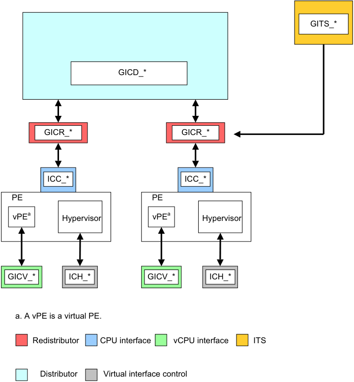
Image text
GITS_
GICD_
GICR_* GICR_
ICC_ ICC_
PE PE
vPE [a] Hypervisor vPE [a] Hypervisor
GICV_ ICH_* GICV_* ICH_*
a. A vPE is a virtual PE.
Redistributor CPU interface vCPU interface ITS
Distributor Virtual interface control
This appendix describes the AXI4-Stream protocol standard message-based interface that the optional GIC Stream Protocol interface uses. It contains the following sections:
-
OverviewA-866 .
-
Signals and the GIC Stream ProtocolA-867 .
-
The GIC Stream ProtocolA-870 .
-
Alphabetic list of command and response packet formatsA-875 . A-865
Appendix A GIC Stream Protocol interface A.1 Overview
A.1 Overview
The GIC Stream Protocol interface describes the optional interface between the IRI and the PE, more specifically that between the Redistributor and the associated CPU interface. The interface supports independent development of an IRI and a PE, that includes System register support for the CPU interface. Arm recommends that a GIC implementation uses this stream protocol interface.
A communication channel that provides a packet interface, based on the AMBA 4 AXI-4 Stream Protocol, is required for each direction:
-
From the Redistributor to the CPU interface.
-
From the CPU interface to the Redistributor.
See Signals and the GIC Stream ProtocolA-867 for more information.
A.1.1 Terminology
The direction of communication for commands is referred to as downstream or upstream, where:
-
Downstream is the direction associated with a command that is initiated by a Redistributor and sent to its associated CPU interface.
-
Upstream is the direction associated with a command initiated by a CPU interface and sent to its associated Redistributor.
Note This terminology can also be applied to communication within an IRI, that is between the Distributor and Redistributor. In this case:
-
An upstream transfer is a transfer from a Redistributor to the Distributor.
-
A downstream transfer is a transfer from the Distributor to a Redistributor. A-866
Appendix A GIC Stream Protocol interface A.2 Signals and the GIC Stream Protocol
A.2 Signals and the GIC Stream Protocol
The GIC Stream Protocol interface is based on the unidirectional AXI4-Stream Interface. Therefore, to support bidirectional communication, the GIC Stream Protocol interface consists of an AXI4-Stream Protocol Interface in each direction, that is:
-
A downstream AXI4-Stream Interface containing connections from one or more Redistributors to an equivalent number of CPU interfaces. On this interface, the Redistributor is the Requester and the CPU interface is the Completer.
-
An upstream AXI4-Stream Interface containing connections from one or more CPU interfaces to an equivalent number of Redistributors. On this interface, the CPU interface is the Requester and the Redistributor is the Completer.
Multiple packets on an AXI4-Stream Interface cannot be interleaved, that is, only one packet can be transferred in each direction at a given time.
Figure A-1 shows an example implementation of the GIC Stream Protocol interface.
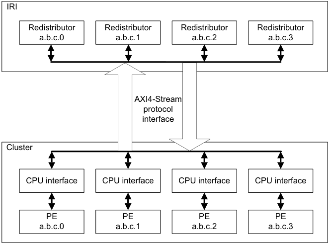
Image text
IRI
Redistributor Redistributor Redistributor Redistributor
a.b.c.0 a.b.c.1 a.b.c.2 a.b.c.3
AXI4-Stream
protocol
interface
Cluster
CPU interface CPU interface CPU interface CPU interface
PE PE PE PE
a.b.c.0 a.b.c.1 a.b.c.2 a.b.c.3
The GIC architecture requires a GIC implementation to include a Redistributor corresponding to each connected CPU interface, and defines an enumeration notation for identifying PEs. On any AXI4-Stream Interface, each Redistributor must only communicate with its corresponding CPU interface.
The AMBA[®] 4 AXI4-Stream Protocol Specification defines a packet as a group of bytes that are transported together across an AXI4-Stream interface.
An interconnect between an IRI and a CPU interface must ensure that the stream packet sequence is transferred over the stream protocol interface in the same order in which it was created.
A.2.1 Signals
The interface requires a global clock, ACLK , and a reset signal, ARESETn .
For the GIC Stream Protocol, each stream interface is identified by a prefix to the AXI-4 signal names:
-
Downstream signals from a Redistributor to the CPU interface are prefixed with the letters IRI .
-
Upstream signals from the CPU interface to a Redistributor are prefixed with the letters ICC . A-867
Appendix A GIC Stream Protocol interface A.2 Signals and the GIC Stream Protocol
Table A-1 shows the GIC Stream Protocol interface from the Redistributor to the downstream CPU interface.
Table A-1 Redistributor to downstream CPU interface
| Signala | Description |
|---|---|
| IRITVALID | When set to 1, this signal indicates that the Requester is driving a valid transfer. |
| IRITREADY | When set to 1, this signal indicates that the Completer can accept a transfer in the current cycle. |
| IRITDATA[BN:0] | The interface data path. |
| IRITLAST | When set to 1, this signal indicates the final transfer of a packet. |
| IRITDEST[N:0] | When more than one PE is supported by the stream interface, this signal identifies the target CPU interface to provide routing information for the stream. Otherwise this signal is not required. |
- a. These signals were previously prefixed with ICD in the preliminary architecture information.
Table A-2 shows the GIC Stream Protocol interface from the CPU interface to the upstream Redistributor.
Table A-2 CPU interface to upstream Redistributor interface
| Signal | Description |
|---|---|
| ICCTVALID | When set to 1, this signal indicates that the Requester is driving a valid transfer. |
| ICCTREADY | When set to 1, this signal indicates that the Completer can accept a transfer in the current cycle. |
| ICCTDATA[BN:0] | The interface data path. |
| ICCTLAST | When set to 1, this signal indicates the final transfer of a packet. |
| ICCTID[N:0] | When more than one PE is supported by the stream interface, this signal identifies the originating CPU interface, to provide routing information for the stream. Otherwise this signal is not required. |
-
In Table A-1 and Table A-2:
-
BN is the number associated with the most significant bit on a datapath that is required to be an integral number of bytes wide.
-
N is the value log(base2) M rounded up to the nearest integer, where M is the number of PEs supported by the interface.
-
Values of TDEST and TID must be allocated sequentially without gaps, in order of ascending affinity.
For further information about the signals used by the GIC Stream Protocol interface, and for details about handshaking, see AMBA[®] 4 AXI4-Stream Protocol Specification .
A.2.2 Packet format
The GIC architecture issues packets across the GIC Stream Protocol interface where the initial half-byte of a packet indicates the packet type.
The declared size of a packet is always a multiple of the implemented datapath width used for the stream transfer. Where the number of bytes required by a packet is less than the overall packet size, the unused bytes are marked as reserved and filled with the value zero. A-868
Appendix A GIC Stream Protocol interface A.2 Signals and the GIC Stream Protocol
Supported INTID sizes
The GIC architecture supports 16-bit and 24-bit INTID fields. Where the INTID is an argument within a packet, the ID length field in the packet header defines which ID format is used, as follows:
-
ID length == 0 for 16-bit INTIDs.
-
ID length == 1 for 24-bit INTIDs.
Note Reserved fields must be transmitted.
A downstream control command is used during interface initialization to inform a CPU interface whether the IRI supports 24-bit INTIDs.
For a 24-bit INTID where bits[23:16] have the value zero, the stream interface is allowed to identify and transfer the packet with a 16-bit INTID field.
A protocol error occurs when a PE generates a packet using a 24-bit INTID with nonzero bits[23:16] and the IRI only supports 16-bit INTIDs.
The Downstream Control Acknowledge command from the CPU interface returns the maximum INTID lengths supported by both the Redistributor and the CPU interface. The Redistributor and the CPU interface must not send a command that contains an INTID exceeding this length.
When both the Redistributor and the CPU interface support an INTID length larger than 16 bits, but the value of an INTID in a particular packet can only be encoded using 16 bits, it is permissible to send a 16-bit value, where ID length == 0b00.
Software generation of protocol errors and packet errors
Software programming must never be permitted to cause a hardware protocol error because this might result in the PE or GIC becoming non-operational.
Where errors exist in the values of fields within packets, this is called a packet error . Protocol and packet errors can cause UNPREDICTABLE behavior. The manner in which these errors are reported is IMPLEMENTATION DEFINED.
Hardware generation of packet errors
If packets are sent that do not correspond to the architected format described in this specification, and the incorrect format is not the result of software misprogramming, then the architecture makes no guarantees about the behavior of the GIC. In such cases, the GIC can become non-operational in many ways, and this might result in the system hanging, data corruption, or any other effect. Physical damage to the system cannot be precluded in some implementations.
In high reliability systems, implementations might choose to report such cases using IMPLEMENTATION DEFINED system errors, but this is outside the scope of the architecture. A-869
Appendix A GIC Stream Protocol interface A.3 The GIC Stream Protocol
A.3 The GIC Stream Protocol
The GIC Stream Protocol supports two types of packet:
-
Command packets for control actions.
-
Response packets that acknowledge command packets.
Note The Activate and Release commands are designated as a command, but also provide a response semantic to the Set and VSet commands. See the Activate and Release commands for more details.
Table A-3 shows a summary of the downstream Redistributor commands.
Table A-3 Redistributor commands
| Parameters in the | Data in | |||
|---|---|---|---|---|
| Command | ID | first 16-bit transfer | subsequent transfers | Description |
| Clear | 0x3 | Bits[7:6]: ID length | INTID | Resets a specified pending physical interrupt. |
| Downstream | 0x8 | Bit[15:12]: Length | Length bytes of | Writes data to the CPU interface. |
| Control | Bits[11:4]: Identifier | data | Length must be greater than 0 and less than 9. | |
| Quiesce | 0x4 | - | - | Requests that the CPU interface enters the quiescent state. |
| Set | 0x1 | Bits[15:8]: Priority Bits[7:6]: ID length Bit[5] GrpMod Bit[4]: Group | INTID | Sets the highest priority pending physical interrupt for a PE. |
| VClear | 0x7 | Bits[7:6]: ID length | Virtual INTID | Resets a specified pending virtual interrupt. This command is provided in GICv4 only. |
| VSet | 0x6 | Bits[15:8]: Priority Bits[7:6]: ID length Bit[4]: Group | Virtual INTID | Sets the highest priority pending virtual interrupt for a VM. This command is provided in GICv4 only. |
Table A-4 shows a summary of the upstream Redistributor responses.
Table A-4 Redistributor responses
| Parameters in the | Data in | |||
|---|---|---|---|---|
| Response | ID | first 16-bit transfer | subsequent transfers | Description |
| Activate | 0xC | Bit[4]: V | - | Acknowledges that the Redistributor received anActivate |
| Acknowledge | command, and confirms that the effects of the activate are visible. | |||
| Arm IHI 0069G |
A-870
Appendix A GIC Stream Protocol interface A.3 The GIC Stream Protocol
Table A-4 Redistributor responses (continued)
| Parameters in the | Data in | |||
|---|---|---|---|---|
| Response | ID | first 16-bit transfer | subsequent transfers | Description |
| Deactivate | 0xA | - | - | Acknowledges that the Redistributor received a |
| Acknowledge | Deactivatecommand, and confirms that the effects of the deactivate are visible. | |||
| Generate SGI | 0x9 | - | - | Acknowledges that the Redistributor received aGenerate |
| Acknowledge | SGIcommand, and that the effects of the command are guaranteed to become visible to other PEs. | |||
| Upstream | 0xB | - | - | Acknowledges receipt of anUpstream Controlcommand, |
| Control | and confirms that the effects of the write operation are | |||
| Acknowledge | visible. |
All other command and response IDs are reserved. If the Redistributor receives a reserved ID, this constitutes a protocol error, see Software generation of protocol errors and packet errorsA-869 .
Table A-5 shows a summary of all the CPU interface commands.
| Table A-5 CPU interface commands | ||||
|---|---|---|---|---|
| Command | ID | Parameters in the first 16-bit transfer | Data in subsequent transfers | Description |
| Activate | 0x1 | Bits[7:6]: ID length Bit[4]: V | INTID | A pending to active notification request as a result of an interrupt acknowledge on the CPU interface. |
| Deactivate | 0x6 | Bits[10:8]: Groups Bits[7:6]: ID length | INTID | Deactivate request for a specified interrupt. |
| Generate SGI | 0x7 | Bits[59:56]: RS Bits[15:12] SGInum Bit[9]: RSV Bit[8]: A3V Bits[7]: IRM Bit[6]: NS Bit[5:4]: SGT | Affinity Routing Values (A0 to A3) | Requests that the Redistributor issues an SGI. |
| Upstream Control | 0x8 | Bits[15:12]: Length Bits[11:4]: Identifier | Length bytes of data | A system control command that might, for example, pass the configuration status to the Redistributor. Length must be greater than 0 and less than 9. |
| A-871 |
Appendix A GIC Stream Protocol interface A.3 The GIC Stream Protocol
Table A-6 shows a summary of all the CPU interface responses.
Table A-6 CPU interface responses
| Parameters in the | Data in | |||
|---|---|---|---|---|
| Response | ID | first 16-bit transfer | subsequent transfers | Description |
| Clear Acknowledge | 0x4 | Bit [4]: V | - | Acknowledges that the CPU interface received aClear command for a specified interrupt. |
| Downstream | 0xB | - | - | Acknowledges that the CPU interface received a |
| Control Acknowledge | Downstream Controlcommand from the Redistributor. | |||
| Quiesce | 0x9 | - | - | Acknowledges aQuiescecommand, and confirms that |
| Acknowledge | the Redistributor to CPU interface is in the quiescent state. | |||
| Release | 0x3 | Bits[7:6] ID length Bit[4]: V | INTID | Releases control of an interrupt when the CPU interface cannot handle the interrupt, and provides a reason for the release. |
All other command and response IDs are reserved. If the CPU interface receives a reserved ID, this constitutes a protocol error, see Software generation of protocol errors and packet errorsA-869 .
A command packet has an equivalent handshake response packet that acknowledges the command. There are two exceptions to this rule:
-
The Clear and VClear commands are both acknowledged by a Clear Acknowledge response with a bitfield in the header that indicates which command is acknowledged.
-
The Set and VSet command packets are acknowledged by a Release response or an Activate command. This means that the Activate command also has the semantics of a response with respect to the Set and VSet commands. When an Activate command is used, the Redistributor acknowledges that command with an Activate Acknowledge response. Release, Activate, and Activate Acknowledge packets all have a bitfield in the header that indicates whether the response is to a Set or VSet command.
-
Responses to a Set or VSet command are dependent on system contexts and events on the CPU interface. A Release response occurs when a pending interrupt that has been forwarded to the CPU interface cannot be maintained as pending or activated by the CPU interface. This can occur, for example, when:
-
The interrupt group of the INTID is disabled.
-
The highest pending physical interrupt is updated by a Set command before it is activated.
-
The highest pending virtual interrupt is updated by a VSet command before it is activated.
-
A.3.1 Rules associated with the downstream Redistributor commands
The following rules affect the generation of Redistributor commands:
-
When GICR_WAKER.ProcessorSleep == 0, the first packet that is issued to the CPU interface must be a Downstream Control packet. This packet communicates the number of supported Security states, together with the physical and virtual INTID lengths that the GIC Stream Protocol interface supports.
-
There can never be more than one outstanding Downstream Control command, and a Redistributor must only generate response packets until the Downstream Control command is acknowledged.
-
On receipt of a Set command, a CPU interface is required to release the previous pending physical interrupt back to the Redistributor.
-
Unless restricted by another rule in this section, two Set commands can be generated and outstanding at the same time, and the Redistributor must be able to accept an Activate command for a physical interrupt when a Set command is transferred. A-872
Appendix A GIC Stream Protocol interface A.3 The GIC Stream Protocol
-
On receipt of a VSet command, a CPU interface is required to release the previous pending virtual interrupt back to the Redistributor.
-
A VSet command must only be generated when the Redistributor is able to accept an Activate command for a virtual interrupt while the VSet command is being transferred.
-
The Redistributor can only issue a single Clear to the CPU interface and must wait for a Clear Acknowledge (with V == 0) before another can be issued. While a Clear is outstanding, no further “Physical Interrupt” packets except acknowledgements can be issued to the CPU interface.
-
The Redistributor can only issue a single VClear to the CPU interface and must wait for a Clear Acknowledge (with V == 1) before another may be issued. While a VClear is outstanding, no further “Virtual Interrupt” packets can be issued to the CPU interface.
-
There can never be more than one outstanding Quiesce command, and a Redistributor must only generate response packets until the Quiesce command is acknowledged with a Quiesce Acknowledge.
-
A Redistributor must not send a VSet or VClear command to a CPU interface that does not support GICv4. The mechanism for determining whether GICv4 is supported is IMPLEMENTATION DEFINED.
-
A VSet and VClear command can specify an INTID:
-
For GICv4.0, in the LPI range.
-
For GICv4.1, in the LPI or SGI range.
-
-
A CPU interface does not send a Deactivate in response to the deactivation of vSGI received in response to a VSet.
A.3.2 Rules associated with the upstream CPU interface commands
The following rules affect the generation of CPU interface commands:
-
There can never be more than one outstanding Upstream Control command, and a CPU interface must wait for an Upstream Control Acknowledge before issuing another Upstream Control command.
-
There can never be more than one outstanding Deactivate command. This means that a CPU interface must wait for a Deactivate command to be acknowledged before issuing another Deactivate command. The CPU interface can continue to send other commands before receiving the Deactivate Acknowledge response.
-
There can never be more than one outstanding Generate SGI command. This means that a CPU interface must wait for a Generate SGI command to be acknowledged before issuing another Generate SGI command. The CPU interface can continue to send other commands before receiving the Generate SGI Acknowledge response.
-
Before issuing a Clear Acknowledge response with the V bit set to 0, the CPU interface must issue any Release commands that are required to move the physical interrupt specified in the Clear command to the inactive state on the CPU interface.
-
Before issuing a Clear Acknowledge response with the V bit set to 1, the CPU interface must issue any Release commands that are required to move the virtual interrupt specified in the VClear command to the inactive state on the CPU interface.
-
Before issuing a Quiesce Acknowledge response, all other outstanding commands from the Redistributor must be acknowledged, and a Release command must remove any pending interrupts on the CPU interface.
-
A CPU interface always responds to Set commands in the order SETs are received.
-
A CPU interface always responds to Virtual Set (VSet) commands in the order VSet commands are received.
-
A Release command with V==1 can specify an INTID:
- For GICv4.0 in the LPI range.
-
For GICv4.1 in the LPI or SGI range. A-873
Appendix A GIC Stream Protocol interface A.3 The GIC Stream Protocol
- For a Clear, or VClear, with INTID=1023, the CPU interface responds with an acknowledge, but otherwise ignores the command.
Priority-based routing
When ICC_CTLR_EL3.PMHE == 0, or ICC_CTLR_EL1.PMHE == 0:
- The CPU interface must not issue a Release command for a pending SPI because the priority of the SPI is equal to or less than that indicated by ICC_PMR_EL1.
Note The CPU interface might still issue a Release command for a pending SPI for other reasons, such as the SPI belonging to a group that is disabled in the CPU interface, or in response to receipt of a Clear command from the IRI.
When ICC_CTLR_EL3.PMHE == 1 or ICC_CTLR_EL1.PMHE == 1:
-
The CPU interface must issue an Upstream Control command, with the identifier 0x02, when the PE successfully writes to ICC_PMR_EL1:
- If multiple writes to ICC_PMR_EL1 occur before the CPU interface issues the Upstream Control command, the GIC can combine these writes into a single command.
-
The CPU interface can issue a Release command for a pending SPI with a priority that is equal to or less than the value in ICC_PMR_EL1, if the Set command was received between the architectural execution of the instruction that updated ICC_PMR_EL1 and the receipt of the Upstream Control Acknowledge command that indicates that the new ICC_PMR_EL1 value has been observed. Whether a Release is generated in this situation is IMPLEMENTATION DEFINED.
-
The CPU interface must not issue a Release command for a pending SPI with a priority that is greater than the value in ICC_PMR_EL1 if the Set command was not received between the architectural execution of the instruction that updated ICC_PMR_EL1 and the receipt of the Upstream Control Acknowledge that indicates that the new ICC_PMR_EL1 value has been observed.
Note The CPU interface might still issue a Release command for a pending SPI for other reasons, such as the SPI belonging to a group that is disabled in the CPU interface or in response to receipt of a Clear command from the IRI. A-874
Appendix A GIC Stream Protocol interface A.4 Alphabetic list of command and response packet formats
A.4 Alphabetic list of command and response packet formats
This subsection lists all the command and response packet formats in alphabetical order. The heading for each command or response subsection includes a label, ICC or IRI, that indicates the agent that generated the packet. A-875
Appendix A GIC Stream Protocol interface A.4 Alphabetic list of command and response packet formats
A.4.1 Activate (ICC)
The CPU interface sends an Activate command when acknowledging an interrupt. When the Redistributor receives the Activate command, it sets the interrupt to the active state. The CPU interface must send an Activate command only when Redistributor action is required, as follows:
-
For SPIs, SGIs, and PPIs, where the Redistributor must clear the pending bit for edge-triggered interrupts, and set the active bit.
-
For LPIs where the Redistributor must clear the pending bit.
The Activate command generated by the CPU interface, unlike other commands, also acts as a response to a Set or VSet command:
- A Set or VSet command results in a Release response or Activate command in finite time. The amount of time is determined by when the pending interrupt changes its state within the CPU interface. An Activate command acknowledges the original Set command. The Activate command is itself acknowledged using an Activate Acknowledge response from the Redistributor.
Figure A-2 shows the Activate command format.
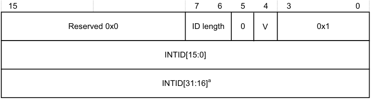
15 7 6 5 4 3 0
Reserved 0x0 ID length 0 V 0x1
INTID[15:0]
INTID[31:16] [a]
- a. If the command includes this field, bits[31:24] are 0.
Figure A-2 Activate
In Figure A-2:
-
ID length indicates the number of INTID bits the Activate command includes. See Supported INTID sizesA-869 for more information.
-
V indicates the original command to which the Activate command corresponds:
-
0 The Activate corresponds to a Set command.
-
1 The Activate corresponds to a VSet command.
-
-
INTID is the value that the CPU interface returns after a valid read of ICC_IAR0_EL1, ICC_IAR1_EL1, or GICC_IAR.
Note
During legacy operation, the INTID that is returned for SGIs includes the source PE in the GICC_IAR.Source_CPU_ID field.
A.4.2 Activate Acknowledge (IRI)
The Redistributor sends an Activate Acknowledge response to confirm receipt of an Activate command, and confirms that the effects of the activate operation are visible to the Redistributor and other PEs. Figure A-3A-877 shows the Activate Acknowledge response format. A-876
Appendix A GIC Stream Protocol interface A.4 Alphabetic list of command and response packet formats
| 15 | 4 5 | 4 5 | 3 0 | |
|---|---|---|---|---|
| Reserved 0x0 | V | 0xC |
Figure A-3 Activate Acknowledge
In Figure A-3, V indicates the original command to which the Activate Acknowledge corresponds: 0b0 The Activate Acknowledge corresponds to a Set command. 0b1 The Activate Acknowledge corresponds to a VSet command.
Note There is no requirement for ActivateAcknowledge commands to be issued in the same order as the Activate command to which they are responding. A-877
Appendix A GIC Stream Protocol interface A.4 Alphabetic list of command and response packet formats
A.4.3 Clear (IRI)
The Clear command clears the specified pending interrupt. Figure A-4 shows the Clear command format.

15 8 7 6 5 4 3 0
Reserved 0x0 ID length 0 0 0x3
INTID[15:0]
INTID[31:16] [a]
a. If the command includes this field, bits[31:24] are 0.
Figure A-4 Clear
In Figure A-4:
-
ID length indicates the number of INTID bits that the Clear command includes. See Supported INTID sizesA-869 for more information.
-
INTID identifies the interrupt to be cleared.
The CPU interface must always respond to a Clear command with a Clear Acknowledge response where V == 0.
If the interrupt is pending in the CPU interface, the CPU interface must issue a Release response, or an Activate response that remains outstanding for the interrupt before it issues a Clear Acknowledge command.
If the interrupt is not pending or present on the CPU interface, the Clear command has no effect. However, the CPU interface must still issue a Clear Acknowledge response.
Note A Clear command with INTID = 1023 has no effect, but a Clear Acknowledge response must still be generated.
A.4.4 Clear Acknowledge (ICC)
The CPU interface sends a Clear Acknowledge response to acknowledge the receipt of a Clear or VClear command. Figure A-5 shows the Clear Acknowledge response format.

15 8 7 6 5 4 3 0
Reserved 0x0 0 0 0 V 0x4
Figure A-5 Clear Acknowledge
In Figure A-5, V indicates the original command to which the Clear Acknowledge corresponds:
0 The Clear Acknowledge corresponds to a Clear command. 1 The Clear Acknowledge corresponds to a VClear command.
Note No INTID field is required for this command because only a single Clear can be outstanding for a CPU interface at any time. A-878
Appendix A GIC Stream Protocol interface A.4 Alphabetic list of command and response packet formats
A.4.5 Deactivate (ICC)
The Deactivate command deactivates an interrupt, provided the initiating Exception level and Security state can access the interrupt group to which the INTID belongs. The Redistributor sends a Deactivate Acknowledge in response to a Deactivate command. Figure A-6 shows the Deactivate command format.
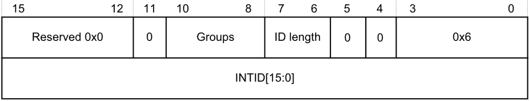
15 12 11 10 8 7 6 5 4 3 0
Reserved 0x0 0 Groups ID length 0 0 0x6
INTID[15:0]
Figure A-6 Deactivate
In Figure A-6:
-
Groups indicates the interrupt groups that the initiating Exception level and Security state are permitted to modify:
-
Bit[10] When this bit is set to 1, Secure Group 1 interrupts can be modified.
-
Bit[9] When this bit is set to 1, Non-secure Group 1 interrupts can be modified. Bit[8] When this bit is set to 1, Group 0 interrupts can be modified.
-
Note When sending a Deactivate command, at least one of the Groups bits must be set to 1. A protocol error occurs if none of these bits are set to 1.
-
ID length indicates the number of INTID bits the Deactivate command includes. See Supported INTID sizesA-869 for more information. The Deactivate command applies only to SPIs, PPIs, and SGIs, each of which has INTIDs no higher than 8192. This field must therefore be set to 0b00, indicating a 16-bit INTID.
-
INTID is the 32-bit value read from the corresponding interrupt acknowledge cycle that is presented in the write to ICC_EOIR0_EL1 or ICC_EOIR1_EL1.
Note There is no requirement for the CPU interface to have received the corresponding Activate Acknowledge command before sending the Deactivate command.
When System register access is enabled for the initiating Exception level and Security state, one of the Groups bits is set according to the rules in Groups field when System register access is enabledA-880 .
Note In an implementation that supports two Security states, for Secure EL1 to be permitted to handle Group 1 interrupts, that is, IRQs not taken to EL3, both bit[9] and bit[10] must be set to 1.
When System register access is not enabled for the initiating Exception level and Security state, the Groups field is set according to the Security state of the initiating Exception level. That is, bit [9] is set to 1 for Non-secure write access, and bits [10:8] are all set to 1 for Secure write access. In an implementation that supports only a single Security state, write accesses that result in the generation of a Deactivate command are treated as Secure writes.
In an implementation that supports two Security states, Group 0 and Secure Group 1 interrupts can be modified only from a Secure initiating Exception level. This includes EL3, regardless of the setting of SCR_EL3.NS. In an implementation that supports only a single Security state, the Redistributor can ignore bit[10]. A-879
Appendix A GIC Stream Protocol interface A.4 Alphabetic list of command and response packet formats
Note The Redistributor must send a Deactivate Acknowledge in response to a Deactivate command.
-
If affinity routing is enabled for an interrupt group, the Redistributor must acknowledge, but otherwise ignore, any Deactivate command with an ID in the range 1019 < INTID < 8192.
-
If affinity routing is not enabled for an interrupt group, the Redistributor must acknowledge, but otherwise ignore any Deactivate command with an ID in the range 1019 < INTID < 8192 where bits [9:4] are not 0. That is, it might issue Deactivate packets for SGIs with a non-zero CPU number in bits[12:10] of GICC_IAR.
-
If affinity routing is not enabled for an interrupt group and the ID specifies an SGI, and the PE specified by the CPU number in bits[12:10] does not support operation when affinity routing is not enabled, the Redistributor must acknowledge but otherwise ignore the Deactivate command.
Groups field when System register access is enabled
When System register access is enabled for the initiating Exception level and Security state, the following pseudocode describes the rules for specifying the value of the Groups field:
// This invalidates any caches containing the configuration data
for all interrupts in the
// collection. Over invalidation is permitted.
InvalidateCollectionCaches(UInt(cmd.ICID));
IncrementReadPointer();
return;
A.4.6 Deactivate Acknowledge (IRI)
The Redistributor sends a Deactivate Acknowledge response to confirm receipt of a Deactivate command, and to confirm that the effects of the deactivate operation are visible to the Redistributor and other PEs. Figure A-7 shows the Deactivate Acknowledge response format.
15 4 3 0
Reserved 0x0 0xA
Figure A-7 Deactivate Acknowledge
A.4.7 Downstream Control (IRI)
The Downstream Control command transfers a specified number of bytes of data to the CPU interface. Figure A-8 shows the Downstream Control command format.
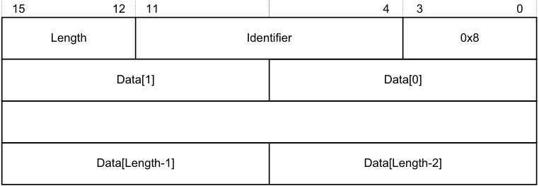
15 12 11 4 3 0
Length Identifier 0x8
Data[1] Data[0]
Data[Length-1] Data[Length-2]
Figure A-8 Downstream Control
In Figure A-8:
-
Length indicates the number of bytes of valid data appended to the 2 byte header.
- If this field specifies a number of bytes that is not exactly divisible by the interface width, as Signals and the GIC Stream ProtocolA-867 describes, any surplus bytes beyond this specified length in the last transfer must be zero. The CPU interface must ignore such bytes. A-881
Appendix A GIC Stream Protocol interface A.4 Alphabetic list of command and response packet formats
- Identifier is a value that specifies the format of the data provided, and can have the values shown in Table A-7.
Table A-7 Downstream Control Identifier values
| Data value name Identifier value Length | Data value name Identifier value Length | Data value name Identifier value Length | Contents |
|---|---|---|---|
| Settings (configure interface) 0x00 0x1 | Data[0] holds the Redistributor global settings, and these bits have the following meanings: [7:6] VL. Indicates the supported vINTID length. [5:4] PL. Indicates the supported pINTID length. [3:2] Reserved. RES0. [1] RSS. Indicates the value ofGICD_TYPER.RSS. [0] DS. Disable Security. Indicates the value ofGICD_CTLR.DS. Note Bit[0] is set to 1 if the GIC supports only a single Security state. | ||
| Reserved 0x01-0x7F - | - | ||
| IMPLEMENTATION DEFINED 0x80-0xFF - | Reserved forIMPLEMENTATION DEFINEDvariables. | ||
| Note | |||
| Each identifier length. | value can have | a different length, but a particular identifier value must always have the same |
The CPU interface must always respond to a Downstream Control command with a Downstream Control Acknowledge response.
After the CPU interface receives a Downstream Control command where DS == 1, a packet protocol violation occurs if it receives a subsequent Downstream Control command where DS == 0, before an intervening hardware reset.
If a CPU interface receives an IMPLEMENTATION DEFINED value that it cannot interpret, this constitutes a protocol error. See Software generation of protocol errors and packet errorsA-869 .
Note The IMPLEMENTATION DEFINED values of the Downstream Write Command must only be used where the Distributor and the CPU interface interpret the IMPLEMENTATION DEFINED values to mean the same thing. This is typically the case where both components have been produced as part of the same system design.
A.4.8 Downstream Control Acknowledge (ICC)
The CPU interface sends a Downstream Control Acknowledge response to confirm receipt of a Downstream Control command. Figure A-9 shows the Downstream Control Acknowledge response format.
| 15 | 8 | 4 7 6 5 | 4 7 6 5 | 3 0 |
|---|---|---|---|---|
| Reserved 0x0 | VL | PL | 0xB |
Figure A-9 Downstream Control Acknowledge
In Figure A-9:
- VL indicates the virtual INTID length, that is, the supported number of INTID bits. A-882
Appendix A GIC Stream Protocol interface A.4 Alphabetic list of command and response packet formats
- PL indicates the physical INTID length, that is, the supported number of INTID bits.
See Supported INTID sizesA-869 for more information.
VL must be set to the minimum of:
-
The value of VL contained in the first Downstream Control command received after reset.
-
The value that ICH_VTR_EL2.IDbits specifies.
PL must be set to the minimum of:
-
The value of PL contained in the first Downstream Control command received after reset.
-
The value that ICC_CTLR_EL3.IDbits or ICC_CTLR_EL1.IDbits, as appropriate, specifies.
A.4.9 Generate SGI (ICC)
The CPU interface sends a Generate SGI command to the Redistributor to generate an SGI. The Redistributor sends a Generate SGI Acknowledge in response to a Generate SGI command. Figure A-10 shows the Generate SGI command format.
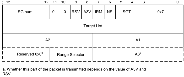
Image text
15 12 11 10 9 8 7 6 5 4 3 0
SGInum 0 0 RSV A3V IRM NS SGT 0x7
Target List
A2 A1
Reserved 0x0 [a] Range Selector A3 [a]
a. Whether this part of the packet is transmitted depends on the value of A3V and
RSV.
-
SGInum indicates the INTID of the SGI to be generated.
-
RSV (Range Selector Valid) indicates whether the RS field is valid:
-
0 RS is RES0.
-
1 RS indicates the affinities covered by Target List.
-
-
A3V indicates whether the command includes an A3 field. When A3V is 0, the packet does not include an A3 field, and the Redistributor must use 0 as the value of A3.When a CPU interface supports the Aff3 field and a write to ICC_SGI0R, ICC_SGI1R or ICC_ASGI1R specifies Aff3 == 0, the resulting packet must clear A3V to zero.
-
IRM indicates the Interrupt Routing Mode to be used. When IRM is set to 1, Target List, A1, A2, and A3 are ignored. The A3V field is RES0.
-
NS indicates whether the Generate SGI command originates from Non-secure state: 0 The command originates from a Secure Execution state. 1 The command originates from a Non-secure Execution state.
-
SGT specifies the register access that caused the Generate SGI command: 0b00 ICC_SGI0R_EL1. 0b01 ICC_SGI1R_EL1. 0b10 ICC_ASGI1R_EL1. 0b11 Reserved. A-883
Appendix A GIC Stream Protocol interface A.4 Alphabetic list of command and response packet formats
When the Redistributor supports two Security states and affinity routing is not enabled for the Secure state in the Redistributor, Generate SGI commands that correspond to Non-secure writes to ICC_SGI0R_EL1 and ICC_ASGI1R_EL1 must be acknowledged and discarded, and must not set an SGI pending.
When the Redistributor supports a single Security state, that is, GICD_CTLR.DS == 1, Generate SGI commands that correspond to Non-secure writes to ICC_SGI0R_EL1 or ICC_ASGI1R_EL1 generate a Group 0 SGI.
-
Target List is the group of target PEs defined by the routing mode. For SGIs, the GIC routing mode defines a group of target PEs, targetlist. This field is treated as defined in ICC_SGI0R_EL1, ICC_SGI1R_EL1, and ICC_ASGI1R_EL1.
-
A1, A2, and A3 are the affinity level values used for generating the set of target PEs. These fields are treated in the same way as the Affinity value fields in ICC_SGI0R_EL1, ICC_SGI1R_EL1, and ICC_ASGI1R_EL1 Whether the A3 field is supported is IMPLEMENTATION DEFINED.
Note In systems where the Redistributor only supports the zero value for A3, the Redistributor must acknowledge any Generate SGI commands where A3V == 1 with a Generate SGI Acknowledge response, but must otherwise ignore the command.
- RS (Range Selector) indicates the affinities covered by Target List. This field is treated as defined in ICC_SGI0R_EL1, ICC_SGI1R_EL1, and ICC_ASGI1R_EL1.
A.4.10 Generate SGI Acknowledge (IRI)
The Redistributor sends a Generate SGI Acknowledge response to confirm that it has received a Generate SGI command from the CPU interface, and that the effects of that command are guaranteed to become visible to other PEs. Figure A-11 shows the Generate SGI Acknowledge response format.

15 4 3 0
Reserved 0x0 0x9
Figure A-11 Generate SGI Acknowledge
Note Receipt of a Generate SGI Acknowledge response by a CPU interface does not guarantee that the corresponding SGI pending state is set, but it does guarantee that the pending state will become set.
A.4.11 Quiesce (IRI)
The Redistributor sends a Quiesce command to request that the CPU interface enters the quiescent state. Figure A-12 shows the Quiesce command format.
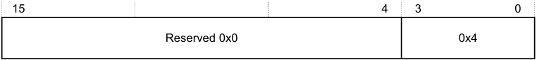
15 4 3 0
Reserved 0x0 0x4
Figure A-12 Quiesce
A CPU interface is quiescent when there are no pending interrupts and all outstanding operations are complete. To ensure quiescence, a CPU interface must:
-
Respond to any outstanding Clear and VClear commands by sending a Clear Acknowledge command.
-
Release any pending virtual or physical interrupts.
-
Ensure it receives an acknowledge response from the Redistributor to indicate completion of all outstanding:
- Generate SGI requests. A-884
Appendix A GIC Stream Protocol interface A.4 Alphabetic list of command and response packet formats
- Activate requests.
- Deactivate requests.
-
Upstream Control.
-
Respond to the Quiesce commands by sending a Quiesce Acknowledge response as the final transfer.
In addition, software must ensure that the Redistributor receives no traffic after the CPU interface sends the Quiesce Acknowledge response. Failure to adhere to this result in UNPREDICTABLE behavior. In practice, because such timing is not predictable, software must ensure that no traffic is generated after the GICR_WAKER.ProcessorSleep bit is set to 1, see Chapter 11 Power Management .
A CPU interface cannot receive a Quiesce command if a Downstream Control Acknowledge response is outstanding. See Rules associated with the downstream Redistributor commandsA-872 for more information.
A.4.12 Quiesce Acknowledge (ICC)
The CPU interface sends a Quiesce Acknowledge response to confirm receipt of a Quiesce command, and to confirm that it is quiescent. Figure A-13 shows the Quiesce Acknowledge response format.

15 4 3 0
Reserved 0x0 0x9
Figure A-13 Quiesce Acknowledge
The Quiesce command acts as a form of barrier. Before sending a Quiesce Acknowledge response, the CPU interface must be quiescent, that is, it must fulfil the requirements for quiescence specified in Quiesce (IRI)A-884 .
A.4.13 Release (ICC)
The CPU interface logic sends a Release response when it cannot handle a particular interrupt. Figure A-14 shows the Release response format.
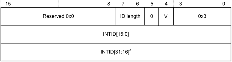
15 8 7 6 5 4 3 0
Reserved 0x0 ID length 0 V 0x3
INTID[15:0]
INTID[31:16] [a]
- a. If the command includes this field, bits[31:24] are 0.
Figure A-14 Release
In Figure A-14:
-
ID length indicates the number of INTID bits the Release response includes. See Supported INTID sizesA-869 for more information.
-
V indicates the original command to which the Release response corresponds:
- 0 The Release corresponds to a Set command. 1 The Release corresponds to a VSet command.
-
INTID is the value that the CPU interface returns after a valid read of ICC_IAR0_EL1 or ICC_IAR1_EL1. A-885
Appendix A GIC Stream Protocol interface A.4 Alphabetic list of command and response packet formats
Note
-
During legacy operation, the INTID that is returned for SGIs includes the source PE in the GICC_IAR.Source_CPU_ID field.
-
If the INTID corresponds to an interrupt that uses the 1 of N model, the Redistributor might forward the interrupt to a different PE or it might send the interrupt to the same PE again. See Priority-based routingA-874 for information about how the PMHE field might affect the 1 of N selection.
If the CPU interface issues a Release response as a result of disabling an interrupt group, Arm recommends that it sends the Upstream Control command that contains the revised interrupt group enable information before issuing the Release response.
A.4.14 Set (IRI)
The Set command sets the highest priority pending interrupt for a PE. The PE has control of the interrupt and might respond to a read of ICC_IAR0_EL1 or ICC_IAR1_EL1 with the INTID. Figure A-15 shows the Set command format.
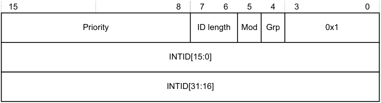
15 8 7 6 5 4 3 0
Priority ID length Mod Grp 0x1
INTID[15:0]
INTID[31:16]
Figure A-15 Set
In Figure A-15:
-
Priority indicates the actual priority of the interrupt, that is, the Secure, unshifted view. Bits corresponding to unimplemented priority bits in the CPU interface are RES0.
-
ID length indicates the number of INTID bits the Set command includes. See Supported INTID sizesA-869 for more information.
-
Mod represents the value of the GICD_IGRPMODR
.Group status bit for the interrupt. -
Grp represents the interrupt group, as indicated by the corresponding GICD_IGROUPR
.Group status bit. -
INTID is the value that the CPU interface returns after a valid read of an ICC_IAR0_EL1 or ICC_IAR1_EL1.
- **Note**- During legacy operation, the INTID that is returned for SGIs includes the source PE in the GICC_IAR.Source_CPU_ID field.
If the Redistributor sends a Set command, the interrupt specified in the command replaces any outstanding highest pending interrupt, that is, the command sets a new highest priority pending interrupt. Where a pending interrupt is replaced, the CPU interface must Release it back to the Redistributor.
The Redistributor must:
-
Ensure that no more than two Set commands that are waiting for a response are outstanding per PE at any time.
-
Send a Set command only if it can accept an Activate command where V == 0.
- Note
An implementation can guarantee this by treating the Set command as outstanding until either a Release command is received for the Set command, or an Activate Acknowledge response is sent for the corresponding Activate. A-886
Appendix A GIC Stream Protocol interface A.4 Alphabetic list of command and response packet formats
-
Never send a Set command when any of the following conditions apply:
-
The INTID is a special interrupt number, that is, 1020-1023.
-
Affinity routing is enabled for an interrupt group and the INTID value is invalid.
-
-
Affinity routing is not enabled for an interrupt group, 1023 < INTID < 8192, and bits[9:4] are non-zero. That is, the Redistributor is permitted to send Set commands for SGIs where bits[12:10] of ICC_IAR0_EL1 or ICC_IAR1_EL1 specify the CPUID of the source PE.
-
Affinity routing is not enabled for an interrupt group, and INTID > 8191
-
The Set command has the same INTID as a previous Set command, unless the Redistributor has received an Activate command or Release response.
The Redistributor must not send a SET command for an interrupt until all of the following are true:
-
All previous outstanding SET commands for that interrupt have been returned through a Release or Activate command.
-
The interrupt is in the pending state, see Interrupt handling state machine .
If the interrupt group is disabled, the CPU interface cannot handle the interrupt, and must Release the interrupt.
A.4.15 Upstream Control (ICC)
This command communicates data to the Redistributor. Figure A-16 shows the Upstream Control command format.
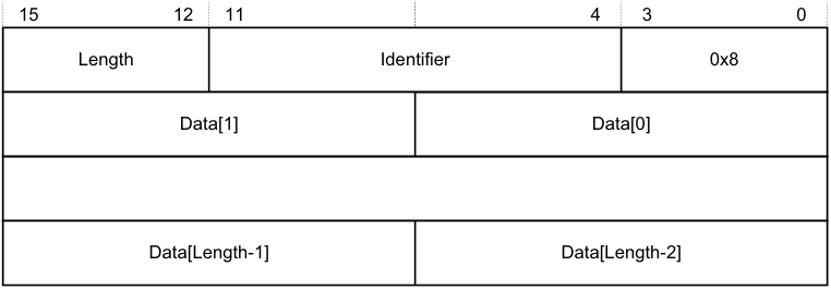
15 12 11 4 3 0
Length Identifier 0x8
Data[1] Data[0]
Data[Length-1] Data[Length-2]
Figure A-16 Upstream Control
In Figure A-16:
-
Length indicates the number of bytes of valid data.
- If this field specifies a number of bytes that is not exactly divisible by the interface width, as Signals and the GIC Stream ProtocolA-867 describes, any surplus bytes beyond this specified length in the last transfer must be zero. The Redistributor must ignore such bytes.
-
Identifier is a value that specifies the format of the data provided. A-887
Appendix A GIC Stream Protocol interface A.4 Alphabetic list of command and response packet formats
Table A-8 shows the possible Identifier values.
| Table A-8 Upstream Control Identifier values | |
|---|---|
| Data value Identifier Length | Contents of Data[0] field |
| Physical interface enables 0x00 0x1 | This value contains the physical CPU interface enable bit values that must be communicated to the Redistributor. Bits [2:0] of Data[0] have the following meanings: [2] EnableGrp1, secure. The value of the Secure copy of ICC_IGRPEN1_EL1.Enable. [1] EnableGrp1, Non-secure. The value of the Non-secure copy of ICC_IGRPEN1_EL1.Enable. [0] EnableGrp0, Secure. The value ofICC_IGRPEN0_EL1.Enable. When GICD_CTLR.DS==1: • EnableGrp1, Secureis always reported as disabled. When GICD_CTLR.DS==0 and the PE supports a single Security state: • PE is always Secure: — EnableGrp1, Non-secureis always reported as disabled. • PE is always Non-secure: — EnableGrp0, Secureis always reported as disabled. — EnableGrp1, Secureis always reported as disabled. To ensure the state of the enable bits can be communicated easily to the Redistributor after powerup, this command must be generated by any write to a physical enable bit. If multiple writes to a physical enable bit occur before the CPU interface issues the command, the GIC can combine these writes into a single command. |
| Virtual interface enables 0x01 0x1 | This value contains the virtual CPU interface enable bit values that must be communicated to the Redistributor. Bits [1:0] of Data[0] have the following meanings: [1] EnableGrp1. The value ofICH_VMCR_EL2.VENG1. [0] EnableGrp0. The value ofICH_VMCR_EL2.VENG0. To ensure the state of the enable bits can be communicated easily to the Redistributor after powerup, this command must be generated by any write to a virtual enable bit. If multiple writes to a virtual enable bit occur before the CPU interface issues the command, the GIC can combine these writes into a single command. Only a CPU interface that supports GICv4 can generate this identifier. Note If EL2 accesses memory-mapped registers, and usesGICH_VMCR, the VM must access GICV_* registers. If the GIC shares state between the GICH_* registers and the ICH_* System registers, it might communicate any change to the virtual enable bits. |
| A-888 |
Appendix A GIC Stream Protocol interface A.4 Alphabetic list of command and response packet formats
Table A-8 Upstream Control Identifier values (continued)
| Data value Identifier Length | Contents of Data[0] field |
|---|---|
| Physical priority 0x02 0x1 | This value contains the current value of the Priority Mask Register (PMR): [7:0] The value written toICC_PMR_EL1. The CPU interface must issue this command when the PE successfully writes to ICC_PMR_EL1andICC_CTLR_EL3.PMHE bit is set to 1. The command must be generated by any successful write that changes the value of ICC_PMR_EL1. If multiple writes toICC_PMR_EL1occur before the CPU interface issues the command, the GIC can combine these writes into a single command. Note • In GIC implementations that use this value, the Redistributor copy of the value must reset to the idle priority, that is,0xF8in cases where only 5 bits of priority are implemented. • If the CPU interface receives aSetcommand with a priority lower than the current value inICC_PMR_EL1before theUpstream Control Acknowledgeis received, the GIC mightReleasethatSetcommand. |
| - 0x03 - 0x07 - | Reserved. |
| - 0x80 - 0xFF - | IMPLEMENTATION DEFINED |
If a Redistributor receives an IMPLEMENTATION DEFINED value that it cannot interpret, this constitutes a protocol error. See Software generation of protocol errors and packet errorsA-869 .
A.4.16 Upstream Control Acknowledge (IRI)
The Redistributor sends an Upstream Control Acknowledge response to confirm receipt of an Upstream Control command, and to confirm that the effects of the write operation are visible to the Distributor. Figure A-17 shows the Upstream Control Acknowledge response format.
| 15 | 4 | 3 0 |
|---|---|---|
| Reserved 0x0 | 0xB |
Figure A-17 Upstream Control Acknowledge
A-889
Appendix A GIC Stream Protocol interface A.4 Alphabetic list of command and response packet formats
A.4.17 VClear (IRI)
The VClear command resets the highest priority pending virtual interrupt.
This command is provided in GICv4 only.
Figure A-18 shows the VClear command format.

15 8 7 6 5 4 3 0
Reserved 0x0 ID length 0 0 0x7
vINTID[15:0]
vINTID[31:16] [a]
- a. If the command includes this field, bits[31:24] are 0.
Figure A-18 VClear
In Figure A-18:
-
ID length indicates the number of vINTID bits the VClear command includes. See Supported INTID sizesA-869 for more information.
-
vINTID identifies the virtual interrupt to be cleared.
The CPU interface must always respond to a VClear command by sending a Clear Acknowledge response where V==1.
If the interrupt is pending in the CPU interface, the CPU interface must issue a Release response, or an Activate response that remains outstanding for the interrupt before it issues a Clear Acknowledge command.
If the interrupt is not pending or present on the CPU interface, the VClear command has no effect. However, the CPU interface must still issue a Clear Acknowledge response.
Note This command does not affect LPIs in the List registers.
A.4.18 VSet (IRI)
The Redistributor sends a VSet command to set a virtual interrupt pending for a VM. The PE has control of the interrupt and can respond to a read of ICC_IAR0_EL1 or ICC_IAR1_EL1 with the vINTID.
This command is provided in GICv4 only.
Figure A-19A-891 shows the VSet command format. A-890
Appendix A GIC Stream Protocol interface A.4 Alphabetic list of command and response packet formats
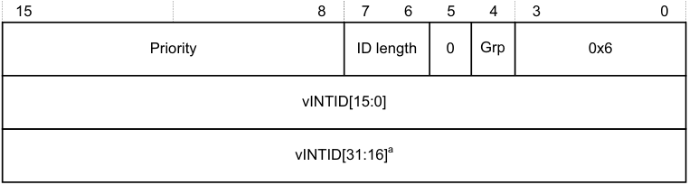
15 8 7 6 5 4 3 0
Priority ID length 0 Grp 0x6
vINTID[15:0]
vINTID[31:16] [a]
- a. If the command includes this field, bits[31:24] are 0.
Figure A-19 VSet
In Figure A-19:
-
Priority indicates the actual priority of the interrupt, that is, the Secure, unshifted view. Bits corresponding to unimplemented priority bits in the CPU interface are RES0.
-
ID length indicates the number of v INTID bits the VSet command includes. See Supported INTID sizesA-869 for more information.
-
Grp represents the interrupt group.
-
vINTID is the value that the CPU interface returns after a valid read of ICC_IAR0_EL1 or ICC_IAR1_EL1. When affinity routing is not enabled for a Security state, the CPUID field in ICC_IAR0_EL1 and ICC_IAR1_EL1 identifies the source PE for SGIs.
The Redistributor sends a VSet command when the virtual interrupt specified by vINTID is set as pending in the resident virtual LPI Pending table. The CPU interface must either activate the virtual interrupt by sending an Activate command where V == 1, or Release the virtual interrupt to the Redistributor.
If the Redistributor sends a VSet command, the interrupt specified in the command always replaces any previous interrupt, that is, the command sets a new highest priority pending interrupt. If the replaced interrupt is still valid and pending, the CPU interface must Release it back to the Redistributor.
The Distributor must:
-
Ensure no more than two VSet commands that are waiting for a response are outstanding per PE at any time.
-
Send a VSet command only if it can accept an Activate command where V == 1.
Note An implementation can guarantee this by treating the VSet command as outstanding until either a Release response is received for the VSet command, or an Activate Acknowledge response is sent for the corresponding Activate command.
-
Never send a VSet command when Virtual INTID < 8192. However, in GICv4.1, VSET and VCLEAR commands can specify an INTID in the SGI ranges as well.
-
Send a VSet command for an interrupt after receipt of either an Activate or a Release command for that particular interrupt.
The CPU interface must Release an interrupt, ensuring that V == 1, if it cannot handle the interrupt for either of the following reasons:
-
The interrupt group is disabled. This includes when the VM interface is disabled, that is, when GICH_HCR.En or ICH_HCR.En, as appropriate, is cleared to 0.
-
The hypervisor is not using the System register interface, that is, when either of the following applies: — During legacy operation, when ICC_SRE_EL2.SRE == 0.
- EL2 is not present.
When the Non-secure copy of ICC_SRE_EL1.SRE == 0, it is UNPREDICTABLE whether the specified virtual interrupt is factored into virtual priority calculations and reads of the GICV_* registers. A-891
Appendix A GIC Stream Protocol interface A.4 Alphabetic list of command and response packet formats A-892
Appendix B Pseudocode Definition
This appendix provides a definition of the pseudocode used in this specification, and lists the helper procedures and support functions used by pseudocode to perform useful architecture-specific jobs. For functions that are referenced in this specification but that are not defined in this appendix, see Arm[®] Architecture Reference Manual, Armv8, for Armv8-A architecture profile .
This appendix contains the following sections:
-
_About Arm pseudocode_B-894.
-
_Data types_B-895.
-
_Expressions_B-899.
-
_Operators and built-in functions_B-901.
-
_Statements and program structure_B-906.
-
_Pseudocode terminology_B-910.
-
_Miscellaneous helper procedures and support functions_B-911. B-893
Appendix B Pseudocode Definition B.1 About Arm pseudocode
B.1 About Arm pseudocode
Arm pseudocode provides precise descriptions of some areas of the architecture. The following sections describe the pseudocode in detail:
-
_Data types_B-895.
-
_Expressions_B-899.
-
_Operators and built-in functions_B-901.
-
_Statements and program structure_B-906.
_Miscellaneous helper procedures and support functions_B-911 describes some pseudocode helper functions that are used by the pseudocode functions that are described elsewhere in this document.
B.1.1 General limitations of Arm pseudocode
The pseudocode statements IMPLEMENTATION_DEFINED, SEE, UNDEFINED, and UNPREDICTABLE indicate behavior that differs from that indicated by the pseudocode being executed. If one of these statements is encountered:
-
Earlier behavior indicated by the pseudocode is only specified as occurring to the extent required to determine that the statement is executed.
-
No subsequent behavior indicated by the pseudocode occurs. This means that these statements terminate pseudocode execution.
For more information, see _Simple statements_B-906. B-894
Appendix B Pseudocode Definition B.2 Data types
B.2 Data types
This section describes:
-
General data type rules .
-
Bitstrings .
-
_Integers_B-896.
-
_Reals_B-896.
-
_Booleans_B-896.
-
_Enumerations_B-896.
-
_Lists_B-897.
-
_Arrays_B-898.
B.2.1 General data type rules
Arm architecture pseudocode is a strongly-typed language. Every constant and variable is of one of the following types:
-
Bitstring.
-
Integer.
-
Boolean.
-
Real.
-
Enumeration.
-
List.
-
Array.
The type of a constant is determined by its syntax. The type of a variable is normally determined by assignment to the variable, with the variable being implicitly declared to be of the same type as whatever is assigned to it. For example, the assignments x = 1, y = ‘1’, and z = TRUE implicitly declare the variables x, y, and z to have types integer, bitstring of length 1, and Boolean, respectively.
Variables can also have their types declared explicitly by preceding the variable name with the name of the type. This is most often done in function definitions for the arguments and the result of the function.
The remaining subsections describe each data type in more detail.
B.2.2 Bitstrings
A bitstring is a finite-length string of 0s and 1s. Each length of bitstring is a different type. The minimum permitted length of a bitstring is 1.
The type name for bitstrings of length N is bits(N). A synonym of bits(1) is bit.
Bitstring constants are written as a single quotation mark, followed by the string of 0s and 1s, followed by another single quotation mark. For example, the two constants of type bit are ‘0’ and ‘1’. Spaces can be included in bitstrings for clarity.
A special form of bitstring constant with ‘x’ bits is permitted in bitstring comparisons. See _Equality and non-equality testing_B-901.
Every bitstring value has a left-to-right order, with the bits being numbered in standard little-endian order. That is, the leftmost bit of a bitstring of length N is bit ( N –1) and its right-most bit is bit 0. This order is used as the most-significant-to-least-significant bit order in conversions to and from integers. For bitstring constants and bitstrings derived from encoding diagrams, this order matches the way they are printed.
Bitstrings are the only concrete data type in pseudocode, in the sense that they correspond directly to the contents of registers, memory locations, and instructions. All of the remaining data types are abstract. B-895
Appendix B Pseudocode Definition B.2 Data types
B.2.3 Integers
Pseudocode integers are unbounded in size and can be either positive or negative. That is, they are mathematical integers rather than what computer languages and architectures commonly call integers. Computer integers are represented in pseudocode as bitstrings of the appropriate length, associated with suitable functions to interpret those bitstrings as integers.
The type name for integers is integer.
Integer constants are normally written in decimal, such as 0, 15, –1234. They can also be written in C-style hexadecimal, such as 0x55 or 0x80000000. Hexadecimal integer constants are treated as positive unless they have a preceding minus sign. For example, 0x80000000 is the integer +2[31] . If –2[31] must be written in hexadecimal, it must be written as –0x80000000.
B.2.4 Reals
Pseudocode reals are unbounded in size and precision. That is, they are mathematical real numbers, not computer floating-point numbers. Computer floating-point numbers are represented in pseudocode as bitstrings of the appropriate length, associated with suitable functions to interpret those bitstrings as reals.
The type name for reals is real.
Real constants are written in decimal with a decimal point. This means 0 is an integer constant but 0.0 is a real constant.
B.2.5 Booleans
A Boolean is a logical TRUE or FALSE value.
The type name for Booleans is boolean. This is not the same type as bit, which is a length–1 bitstring. Boolean constants are TRUE and FALSE.
B.2.6 Enumerations
An enumeration is a defined set of symbolic constants, such as:
enumeration InstrSet {InstrSet_A32, InstrSet_T32, InstrSet_A64};
An enumeration always contains at least one symbolic constant, and a symbolic constant must not be shared between enumerations.
Enumerations must be declared explicitly, although a variable of an enumeration type can be declared implicitly by assigning one of the symbolic constants to it. By convention, each of the symbolic constants starts with the name of the enumeration followed by an underscore. The name of the enumeration is its type name , or type , and the symbolic constants are its possible constants .
Note A Boolean is a pre-declared enumeration that does not follow the normal naming convention and it has a special role in some pseudocode constructs, such as if statements. This means the enumeration of a boolean is:
enumeration boolean {FALSE, TRUE}; B-896
Appendix B Pseudocode Definition B.2 Data types
B.2.7 Lists
A list is an ordered set of other data items, separated by commas and enclosed in parentheses, for example:
(bits(32) shifter_result, bit shifter_carry_out)
A list always contains at least one data item.
Lists are often used as the return type for a function that returns multiple results. For example, this list at the start of this section is the return type of the function Shift_C() that performs a standard Arm shift or rotation, when its first operand is of type bits(32).
Some specific pseudocode operators use lists surrounded by other forms of bracketing than the (…) parentheses. These are:
-
Bitstring extraction operators, that use lists of bit numbers or ranges of bit numbers surrounded by angle brackets <…>.
-
Array indexing, that uses lists of array indexes surrounded by square brackets […].
-
Array-like function argument passing, that uses lists of function arguments surrounded by square brackets […].
Each combination of data types in a list is a separate type, with type name given by listing the data types. This means that the example list at the start of this section is of type (bits(32), bit). The general principle that types can be declared by assignment extends to the types of the individual list items in a list. For example:
(shift_t, shift_n) = (‘00’, 0);
implicitly declares shift_t, shift_n, and (shift_t, shift_n) to be of types bits(2), integer, and (bits(2), integer), respectively.
A list type can also be explicitly named, with explicitly named elements in the list. For example:
type ShiftSpec is (bits(2) shift, integer amount);
After this definition and the declaration:
ShiftSpec abc;
the elements of the resulting list can then be referred to as abc.shift, and abc.amount. This qualified naming of list elements is only permitted for variables that have been explicitly declared, not for those that have been declared by assignment only.
Explicitly naming a type does not alter what type it is. For example, after the above definition of ShiftSpec, ShiftSpec, and (bits(2), integer) are two different names for the same type, not the names of two different types. To avoid ambiguity in references to list elements, it is an error to declare a list variable multiple times using different names of its type or to qualify it with list element names not associated with the name by which it was declared.
An item in a list that is being assigned to can be written as “-” to indicate that the corresponding item of the assigned list value is discarded. For example:
(shifted, -) = LSL_C(operand, amount);
List constants are written as a list of constants of the appropriate types, for example the (‘00’, 0) in the earlier example. B-897
Appendix B Pseudocode Definition B.2 Data types
B.2.8 Arrays
Pseudocode arrays are indexed by either enumerations or integer ranges. An integer range is represented by the lower inclusive end of the range, then .., then the upper inclusive end of the range.
For example:
// The names of the Banked core registers.
enumeration RName {RName_0usr, RName_1usr, RName_2usr, RName_3usr, RName_4usr, RName_5usr,
RName_6usr, RName_7usr, RName_8usr, RName_8fiq, RName_9usr, RName_9fiq,
RName_10usr, RName_10fiq, RName_11usr, RName_11fiq, RName_12usr, RName_12fiq,
RName_SPusr, RName_SPfiq, RName_SPirq, RName_SPsvc,
RName_SPabt, RName_SPund, RName_SPmon, RName_SPhyp,
RName_LRusr, RName_LRfiq, RName_LRirq, RName_LRsvc,
RName_LRabt, RName_LRund, RName_LRmon,
RName_PC};
array
bits(8) _Memory[0..0xFFFFFFFF];
Arrays are always explicitly declared, and there is no notation
for a
constant array. Arrays always contain at least
one element, because:
• Enumerations always contain at least one symbolic constant.
• Integer ranges always contain at least one integer.
Arrays do not usually appear directly in pseudocode. The items that syntactically look like arrays in pseudocode are
usually array-like functions such as R[i], MemU[address, size] or Elem[vector, i, size]. These functions package
up and abstract additional operations normally performed on accesses to the underlying arrays, such as register
banking, memory protection, endian-dependent byte ordering, exclusive-access housekeeping and Advanced SIMD
element processing.
B.3 Expressions
This section describes:
-
General expression syntax .
-
_Operators and functions - polymorphism and prototypes_B-900.
-
_Precedence rules_B-900.
B.3.1 General expression syntax
An expression is one of the following:
-
A constant.
-
A variable, optionally preceded by a data type name to declare its type.
-
The word UNKNOWN preceded by a data type name to declare its type.
-
The result of applying a language-defined operator to other expressions.
-
The result of applying a function to other expressions.
Variable names normally consist of alphanumeric and underscore characters, starting with an alphabetic or underscore character.
Each register described in the text is to be regarded as declaring a correspondingly named bitstring variable, and that variable has the stated behavior of the register. For example, if a bit of a register is defined as RAZ/WI, then the corresponding bit of its variable reads as 0 and ignore writes.
An expression like bits(32) UNKNOWN indicates that the result of the expression is a value of the given type, but the architecture does not specify what value it is and software must not rely on such values. The value produced must not:
-
Return information that cannot be accessed at the current or a lower level of privilege using instructions that are not UNPREDICTABLE and do not return UNKNOWN values.
-
Be promoted as providing any useful information to software.
Note Some earlier documentation describes this as an UNPREDICTABLE value. UNKNOWN values are similar to the definition of UNPREDICTABLE, but do not indicate that the entire architectural state becomes unspecified.
Only the following expressions are assignable. This means that these are the only expressions that can be placed on the left-hand side of an assignment.
-
Variables.
-
The results of applying some operators to other expressions.
The description of each language-defined operator that can generate an assignable expression specifies the circumstances under which it does so. For example, those circumstances might require that one or more of the expressions the operator operates is an assignable expression.
- The results of applying array-like functions to other expressions. The description of an array-like function specifies the circumstances under which it can generate an assignable expression.
Every expression has a data type:
-
For a constant, this data type is determined by the syntax of the constant.
-
For a variable, there are the following possible sources for the data type:
-
An optional preceding data type name.
-
A data type the variable was given earlier in the pseudocode by recursive application of this rule.
-
A data type the variable is being given by assignment, either by direct assignment to the variable, or by assignment to a list of which the variable is a member. B-899
-
Appendix B Pseudocode Definition B.3 Expressions
It is a pseudocode error if none of these data type sources exists for a variable, or if more than one of them exists and they do not agree about the type.
-
For a language-defined operator, the definition of the operator determines the data type.
-
For a function, the definition of the function determines the data type.
B.3.2 Operators and functions - polymorphism and prototypes
Operators and functions in pseudocode can be polymorphic, producing different functionality when applied to different data types. Each resulting form of an operator or function has a different prototype definition. For example, the operator + has forms that act on various combinations of integers, reals, and bitstrings.
One particularly common form of polymorphism is between bitstrings of different lengths. This is represented by using bits(N), bits(M), or similar, in the prototype definition.
B.3.3 Precedence rules
The precedence rules for expressions are:
-
Constants, variables, and function invocations are evaluated with higher priority than any operators using their results.
-
Expressions on integers follow the normal operator precedence rules of exponentiation before multiply/divide before add/subtract , with sequences of multiply/divides or add/subtracts evaluated left-to-right.
-
Other expressions must be parenthesized to indicate operator precedence if ambiguity is possible, but do not have to be if all permitted precedence orders under the type rules necessarily lead to the same result. For example, if i, j, and k are integer variables, i > 0 && j > 0 && k > 0 is acceptable, but i > 0 && j > 0 || k > 0 is not. B-900
Appendix B Pseudocode Definition B.4 Operators and built-in functions
B.4 Operators and built-in functions
This section describes:
-
Operations on generic types .
-
Operations on Booleans .
-
Bitstring manipulation .
-
_Arithmetic_B-904.
B.4.1 Operations on generic types
The following operations are defined for all types.
Equality and non-equality testing
Any two values x and y of the same type can be tested for equality by the expression x == y and for non-equality by the expression x != y. In both cases, the result is of type boolean.
A special form of comparison is defined with a bitstring constant that includes ‘x’ bits in addition to ‘0’ and ‘1’ bits. The bits corresponding to the ‘x’ bits are ignored in determining the result of the comparison. For example, if opcode is a 4-bit bitstring, opcode == ‘1x0x’ is equivalent to opcode<3> == ‘1’ && opcode<1> == ‘0’.
Note
This special form is permitted in the implied equality comparisons in when parts of case … of … structures.
Conditional selection
If x and y are two values of the same type and t is a value of type boolean, then if t then x else y is an expression of the same type as x and y that produces x if t is TRUE and y if t is FALSE.
B.4.2 Operations on Booleans
If x is a Boolean, then !x is its logical inverse.
If x and y are Booleans, then x && y is the result of ANDing them together. As in the C language, if x is FALSE, the result is determined to be FALSE without evaluating y.
If x and y are Booleans, then x || y is the result of ORing them together. As in the C language, if x is TRUE, the result is determined to be TRUE without evaluating y.
If x and y are Booleans, then x ^ y is the result of exclusive-ORing them together.
B.4.3 Bitstring manipulation
The following bitstring manipulation functions are defined:
Bitstring length and most significant bit
If x is a bitstring:
-
The bitstring length function Len(x) returns the length of x as an integer.
-
TopBit(x) is the leftmost bit of x. Using bitstring extraction, this means: TopBit(x)= x<Len(x)–1>.
Bitstring concatenation and replication
If x and y are bitstrings of lengths N and M respectively, then x:y is the bitstring of length N+M constructed by concatenating x and y in left-to-right order. B-901
Appendix B Pseudocode Definition B.4 Operators and built-in functions
If x is a bitstring and n is an integer with n > 0:
-
Replicate(x, n) is the bitstring of length n*Len(x) consisting of n copies of x concatenated together
-
Zeros(n) = Replicate(‘0’, n), Ones(n) = Replicate(‘1’, n).
Bitstring extraction
The bitstring extraction operator extracts a bitstring from either another bitstring or an integer. Its syntax is x<integer_list>, where x is the integer or bitstring being extracted from, and <integer_list> is a list of integers enclosed in angle brackets rather than the usual parentheses. The length of the resulting bitstring is equal to the number of integers in <integer_list>. In x<integer_list>, each of the integers in <integer_list> must be:
-
= 0
-
< Len(x) if x is a bitstring.
The definition of x<integer_list> depends on whether integer_list contains more than one integer:
-
If integer_list contains more than one integer, x<i, j, k,…, n> is defined to be the concatenation: x : x
: x : … : x . -
If integer_list consists of one integer i, x is defined to be:
- If x is a bitstring, ‘0’ if bit i of x is a zero and ‘1’ if bit i of x is a one.
-
If x is an integer, let y be the unique integer in the range 0 to 2^(i+1)–1 that is congruent to x modulo 2^(i+1). Then x is ‘0’ if y < 2^i and ‘1’ if y >= 2^i.
- Loosely, this definition treats an integer as equivalent to a sufficiently long two’s complement representation of it as a bitstring.
In <integer_list>, the notation i:j with i >= j is shorthand for the integers in order from i down to j, with both end values included. For example, instr<31:28> is shorthand for instr<31, 30, 29, 28>.
The expression x<integer_list> is assignable provided x is an assignable bitstring and no integer appears more than once in <integer_list>. In particular, x is assignable if x is an assignable bitstring and 0 <= i < Len(x).
Encoding diagrams for registers frequently show named bits or multi-bit fields. For example, the encoding diagram for the ICC_SGI1R shows its bit<28> as IS. In such cases, the syntax ICC_SGI1R.IS is used as a more readable synonym for ICC_SGI1R<28>.
Logical operations on bitstrings
If x is a bitstring, NOT(x) is the bitstring of the same length obtained by logically inverting every bit of x.
If x and y are bitstrings of the same length, x AND y, x OR y, and x EOR y are the bitstrings of that same length obtained by logically ANDing, ORing, and exclusive-ORing corresponding bits of x and y together.
Bitstring count
If x is a bitstring, BitCount(x) produces an integer result equal to the number of bits of x that are ones. B-902
Appendix B Pseudocode Definition B.4 Operators and built-in functions
Testing a bitstring for being all zero or all ones
If x is a bitstring:
-
IsZero(x) produces TRUE if all of the bits of x are zeros and FALSE if any of them are ones
-
IsZeroBit(x) produces ‘1’ if all of the bits of x are zeros and ‘0’ if any of them are ones.
IsOnes(x) and IsOnesBit(x) work in the corresponding ways. This means:
IsZero(x) = (BitCount(x) == 0) IsOnes(x) = (BitCount(x) == Len(x)) IsZeroBit(x) =
if IsZero(x)
then '1'
else '0' IsOnesBit(x) =
if IsOnes(x)
then '1'
else '0'
Lowest and highest set bits of a bitstring
If x is a bitstring, and N = Len(x):
-
LowestSetBit(x) is the minimum bit number of any of its bits that are ones. If all of its bits are zeros, LowestSetBit(x) = N.
-
HighestSetBit(x) is the maximum bit number of any of its bits that are ones. If all of its bits are zeros, HighestSetBit(x) = –1.
-
CountLeadingZeroBits(x) is the number of zero bits at the left end of x, in the range 0 to N. This means: CountLeadingZeroBits(x) = N – 1 – HighestSetBit(x).
-
CountLeadingSignBits(x) is the number of copies of the sign bit of x at the left end of x, excluding the sign bit itself, and is in the range 0 to N–1. This means:
CountLeadingSignBits(x) = CountLeadingZeroBits(x<N–1:1> EOR x<N–2:0>).
Zero-extension and sign-extension of bitstrings
If x is a bitstring and i is an integer, then ZeroExtend(x, i) is x extended to a length of i bits, by adding sufficient zero bits to its left. That is, if i == Len(x), then ZeroExtend(x, i) = x, and if i > Len(x), then:
ZeroExtend(x, i) = Replicate('0', i–Len(x)) : x
If x is a bitstring and i is an integer, then SignExtend(x, i) is x extended to a length of i bits, by adding sufficient copies of its leftmost bit to its left. That is, if i == Len(x), then SignExtend(x, i) = x, and if i > Len(x), then:
SignExtend(x, i) = Replicate(TopBit(x), i–Len(x)) : x
It is a pseudocode error to use either ZeroExtend(x, i) or SignExtend(x, i) in a context where it is possible that i < Len(x).
Converting bitstrings to integers
If x is a bitstring, SInt(x) is the integer whose two’s complement representation is x:
// SInt()
// ======
integer SInt(bits(N) x)
result = 0;
for i = 0 to N-1
if x<i> == '1' then result = result + 2^i;
if x<N-1> == '1' then result = result - 2^N;
return result;
UInt(x) is the integer whose unsigned representation is x:
// UInt()
// ======
B.4.4 Arithmetic
Most pseudocode arithmetic is performed on integer or real values, with operands being obtained by conversions from bitstrings and results converted back to bitstrings afterwards. As these data types are the unbounded mathematical types, no issues arise about overflow or similar errors.
Unary plus, minus, and absolute value
If x is an integer or real, then +x is x unchanged, –x is x with its sign reversed, and Abs(x) is the absolute value of x. All three are of the same type as x.
Addition and subtraction
If x and y are integers or reals, x+y and x–y are their sum and difference. Both are of type integer if x and y are both of type integer, and real otherwise.
Addition and subtraction are particularly common arithmetic operations in pseudocode, and so it is also convenient to have definitions of addition and subtraction acting directly on bitstring operands.
If x and y are bitstrings of the same length N, so that N = Len(x) = Len(y), then x+y and x–y are the least significant N bits of the results of converting them to integers and adding or subtracting them. Signed and unsigned conversions produce the same result:
x+y = (SInt(x) + SInt(y))<N–1:0> = (UInt(x) + UInt(y))<N–1:0> x–y = (SInt(x) – SInt(y))<N–1:0> = (UInt(x) – UInt(y))<N–1:0>
If x is a bitstring of length N and y is an integer, x+y and x–y are the bitstrings of length N defined by x+y = x + y<N–1:0> and x–y = x – y<N–1:0>. Similarly, if x is an integer and y is a bitstring of length M, x+y and x–y are the bitstrings of length M defined by x+y = x<M–1:0> + y and x–y = x<M–1:0> – y.
Comparisons
If x and y are integers or reals, then x == y, x != y, x < y, x <= y, x > y, and x >= y are equal, not equal, less than, less than or equal, greater than, and greater than or equal comparisons between them, producing Boolean results. In the case of == and !=, this extends the generic definition applying to any two values of the same type to also act between integers and reals.
Multiplication
If x and y are integers or reals, then x * y is the product of x and y. It is of type integer if x and y are both of type integer, and real otherwise.
Division and modulo
If x and y are integers or reals, then x/y is the result of dividing x by y, and is always of type real. B-904
Appendix B Pseudocode Definition B.4 Operators and built-in functions
If x and y are integers, then x DIV y and x MOD y are defined by:
x DIV y = RoundDown(x/y) x MOD y = x – y * (x DIV y)
It is a pseudocode error to use any of x/y, x MOD y, or x DIV y in any context where y can be zero.
Square root
If x is an integer or a real, Sqrt(x) is its square root, and is always of type real.
Rounding and aligning
If x is a real:
-
RoundDown(x) produces the largest integer n so that n <= x
-
RoundUp(x) produces the smallest integer n so that n >= x
-
RoundTowardsZero(x) produces RoundDown(x) if x > 0.0, 0 if x == 0.0, and RoundUp(x) if x < 0.0.
If x and y are both of type integer, Align(x, y) = y * (x DIV y) is of type integer.
If x is of type bitstring and y is of type integer, Align(x, y) = (Align(UInt(x), y))<Len(x)–1:0> is a bitstring of the same length as x.
It is a pseudocode error to use either form of Align(x, y) in any context where y can be 0. In practice, Align(x, y) is only used with y a constant power of two, and the bitstring form used with y = 2^n has the effect of producing its argument with its n low-order bits forced to zero.
Scaling
If n is an integer, 2^n is the result of raising 2 to the power n and is of type real.
If x and n are of type integer, then:
-
x << n = RoundDown(x * 2^n)
-
x >> n = RoundDown(x * 2^(–n)).
Maximum and minimum
If x and y are integers or reals, then Max(x, y) and Min(x, y) are their maximum and minimum respectively. Both are of type integer if x and y are both of type integer, and real otherwise. B-905
Appendix B Pseudocode Definition B.5 Statements and program structure
B.5 Statements and program structure
The following sections describe the control statements used in the pseudocode:
-
Simple statements .
-
_Compound statements_B-907.
-
_Comments_B-909.
B.5.1 Simple statements
Each of the following simple statements must be terminated with a semicolon, as shown.
Assignments
An assignment statement takes the form:
<assignable_expression> =
Procedure calls
A procedure call takes the form:
<procedure_name>(
Return statements
A procedure return takes the form:
return;
and a function return takes the form:
return <expression>;
where <expression> is of the type declared in the function prototype line.
UNDEFINED
This subsection describes the statement:
UNDEFINED;
This statement indicates a special case that replaces the behavior defined by the current pseudocode, apart from behavior required to determine that the special case applies. The replacement behavior is that the Undefined Instruction exception is taken.
UNPREDICTABLE
This subsection describes the statement:
UNPREDICTABLE;
This statement indicates a special case that replaces the behavior defined by the current pseudocode, apart from behavior required to determine that the special case applies. The replacement behavior is UNPREDICTABLE.
SEE…
This subsection describes the statement:
SEE
Appendix B Pseudocode Definition B.5 Statements and program structure
This statement indicates a special case that replaces the behavior defined by the current pseudocode, apart from behavior required to determine that the special case applies. The replacement behavior is that nothing occurs as a result of the current pseudocode because some other piece of pseudocode defines the required behavior. The
It usually refers to another instruction but can also refer to another encoding or note of the same instruction.
IMPLEMENTATION_DEFINED
This subsection describes the statement:
IMPLEMENTATION_DEFINED {};
This statement indicates a special case that replaces the behavior defined by the current pseudocode, apart from behavior required to determine that the special case applies. The replacement behavior is IMPLEMENTATION DEFINED. An optional
B.5.2 Compound statements
Indentation normally indicates the structure in compound statements. The statements contained in structures such as if … then … else … or procedure and function definitions are indented more deeply than the statement itself, and their end is indicated by returning to the original indentation level or less.
Indentation is normally done by four spaces for each level.
if … then … else …
A multi-line if … then … else … structure takes the form:
if <boolean_expression>
then <statement 1> <statement 2> … <statement n>
elsif <boolean_expression>
then <statement a> <statement b> … <statement z>
else <statement A> <statement B> … <statement Z>
The block of lines consisting of elsif and its indented statements is optional, and multiple such blocks can be used.
The block of lines consisting of else and its indented statements is optional.
Abbreviated one-line forms can be used when there are only simple statements in the then part and in the else part, if it is present, such as:
if <boolean_expression>
then <statement 1>
if <boolean_expression>
then <statement 1>
else <statement A>
if <boolean_expression>
then <statement 1> <statement 2>
else <statement A>
Note
In these forms, <statement 1>, <statement 2> and
repeat … until …
A repeat … until … structure takes the form: B-907
Appendix B Pseudocode Definition B.5 Statements and program structure
repeat <statement 1> <statement 2> …
while … do
A while … do structure takes the form:
while <boolean_expression> do <statement 1> <statement 2> … <statement n>
for …
A for … structure takes the form:
for <assignable_expression> = <integer_expr1> to <integer_expr2> <statement 1> <statement 2> …
case … of …
A case … of … structure takes the form:
case
In this structure,
If
Procedure and function definitions
A procedure definition takes the form:
where
Appendix B Pseudocode Definition B.5 Statements and program structure
Note This first prototype line is not terminated by a semicolon. This helps to distinguish it from a procedure call.
A function definition is similar but also declares the return type of the function:
An array-like function is similar but with square brackets:
…
An array-like function also usually has an assignment prototype:
…
B.5.3 Comments
Two styles of pseudocode comment exist:
-
// starts a comment that is terminated by the end of the line
-
/* starts a comment that is terminated by */. B-909
Appendix B Pseudocode Definition B.6 Pseudocode terminology
B.6 Pseudocode terminology
Table B-1 lists the terms used in the body text and the terms used in pseudocode to denote the same concept, throughout this specification.
| Table B-1 Pseudocode terms | |
|---|---|
| Term used in the body text | Term used in pseudocode |
| vPE | VCPU |
| vPEID | VCPUID |
| pINTID | pID |
| vINTID | vID |
| B-910 |
Appendix B Pseudocode Definition B.7 Miscellaneous helper procedures and support functions
B.7 Miscellaneous helper procedures and support functions
The functions described in this section are not part of the pseudocode specification. They are miscellaneous helper procedures and functions used by pseudocode that are not described elsewhere in this document. Each has a brief description and a pseudocode prototype, except that the prototype is omitted where it is identical to the section title.
Note Some variable names used the pseudocode differ from those used in the body text. For a list of the affected variables, see _Pseudocode terminology_B-910.
B.7.1 Helper functions
The functions listed in the following sections are indicated by the hierarchical path names, for example shared/gic/helper:
-
shared/gic/helper/AcknowledgeInterrupt .
-
shared/gic/helper/AcknowledgeVInterrupt .
-
_shared/gic/helper/AlwaysUsingSysRegs_B-912.
-
_shared/gic/helper/Deactivate_B-912.
-
_shared/gic/helper/GetHighestActiveGroup_B-912.
-
_shared/gic/helper/GetHighestActivePriority_B-912.
-
_shared/gic/helper/GICH_SETR_B-912.
-
_shared/gic/helper/GICH_VLPIR_B-912.
-
_shared/gic/helper/INTID_SIZE_B-913.
-
_shared/gic/helper/IntGroup_B-913.
-
_shared/gic/helper/Interrupt_B-913.
-
_shared/gic/helper/IsEL3OrMon_B-913.
-
_shared/gic/helper/IsGrp0Int_B-913.
-
_shared/gic/helper/IsSecureInt_B-913.
-
_shared/gic/helper/PriorityIsHigher_B-914.
-
_shared/gic/helper/SingleSecurityState_B-914.
-
_shared/gic/helper/Special_B-914.
-
_shared/gic/helper/SystemRegisterTrap_B-914.
shared/gic/helper/AcknowledgeInterrupt
// A virtual LPI is the highest priority
vID = GICH_VLPIR.VirtualID<INTID_SIZE-1:0>;
if GICH_VLPIR.Group != '1' then
vID = INTID_SPURIOUS;
elsif lrIndex >= 0 then // lrIndex is valid, that is, positive
vID = ICH_LR_EL2[lrIndex].VirtualID<INTID_SIZE-1:0>;
if (vID != INTID_SPURIOUS && (ICH_LR_EL2[lrIndex].Group != '1' ||
ICH_LR_EL2[lrIndex].State == IntState_Invalid)) then
vID = INTID_SPURIOUS; // If the highest priority isn't group 1, then no interrupt
else
vID = INTID_SPURIOUS;
return ZeroExtend(vID);
shared/gic/helper/AcknowledgeVInterrupt
// AcknowledgeVInterrupt()
// =======================
// Acknowledges vINTID
AcknowledgeVInterrupt(bits(INTID_SIZE) ID);
shared/gic/helper/AlwaysUsingSysRegs
// AlwaysUsingSysRegs() // ===================
// Returns TRUE if the value supplied has bits above the implemented range or
// if the value supplied exceeds the maximum configured size in the
// appropriate GITS_BASERn
boolean VCPUOutOfRange(bits(16) vcpu);
shared/gic/helper/Deactivate
// Deactivate()
// =================
// Deactivates the INTID
Deactivate(bits(INTID_SIZE) INTID);
shared/gic/helper/GetHighestActiveGroup
// GetHighestActiveGroup()
// =======================
// Returns a value indicating the interrupt group of the highest active priority from three
// registers. Returns IntGroup_None if no active priorities.
// Note: having more than one group active at the same priority is UNPREDICTABLE.
IntGroup GetHighestActiveGroup(bits(128) ap0, bits(128) ap1ns, bits(128) ap1s)
shared/gic/helper/GetHighestActivePriority
// GetHighestActivePriority()
// ==========================
// Returns the priority of the highest active priority from three registers, expressed as an 8-bit
// unsigned binary number. Returns 0xFF if no bits are active.
bits(8) GetHighestActivePriority(bits(128) ap0, bits(128) ap1ns, bits(128) ap1s)
shared/gic/helper/GICH_SETR
// GICC_SETR
// ==================
// Holds physical interrupt received from the Distributor
type InterruptType is (
INTID ID,
bits(2) State,
bits(8) Priority,
IntGroup Group
)
InterruptType GICC_SETR;
shared/gic/helper/GICH_VLPIR
// GICH_VLPIR
// ==================
// Holds virtual interrupts received from the Distributor
LRType GICH_VLPIR;
shared/gic/helper/INTID_SIZE
// INTID_SIZE
// ==========
// The number of interrupt ID bits implemented at the Distributor and Redistributor.
// This value is IMPLEMENTATION DEFINED and discoverable from GICD_TYPER.IDbits.
constant integer INTID_SIZE = integer IMPLEMENTATION_DEFINED "Distributor INTID size";
shared/gic/helper/IntGroup
// Int()
// =====
integer Int(bits(N) x, boolean unsigned)
result = if unsigned then UInt(x) else SInt(x);
return result;
shared/gic/helper/Interrupt
// Interrupt()
// ================
constant bits(2) IntState_Invalid = '00';
constant bits(2) IntState_Pending = '01';
constant bits(2) IntState_Active = '10';
constant bits(2) IntState_ActivePending = '11';
shared/gic/helper/IntNeedsDeactivate
// GICv3.0
if (intid < 1020) then return TRUE;
// GICv3.1 extended PPI and SPI ranges
if (!IsSpecial(intid) && !IsLPI(intid) && (ICC_CTLR_EL1.ExtRange == 1)) then return TRUE;
// Otherwise LPI or reserved
return FALSE;
shared/gic/helper/IsEL3OrMon
// IsEL3OrMon()
// =======================
// Returns true if EL3 is using AArch32 and in Monitor mode or
// if EL3 is using AArch64 and PSTATE.EL = 3
boolean IsEL3OrMon();
shared/gic/helper/IsGrp0Int
// IsGrp0Int()
// =======================
// Returns TRUE if the INTID is in Group 0
boolean IsGrp0Int(bits(INTID_SIZE) ID);
shared/gic/helper/IsSecureInt
// IsSecureInt()
// =============
// Returns true if GICD_CTLR.DS == 0 and ID
// is a Group 0 or Secure Group 1 INTID
shared/gic/helper/IsSGI
// IsSGI()
// =======================
// boolean IsSGI(bits(INTID_SIZE) intID)
return UInt(intID) < 16;
shared/gic/helper/PriorityIsHigher
// PriorityIsHigher()
// ===========================
// Returns true if the first priority is higher than the second priority.
boolean PriorityIsHigher(bits(8) first, bits(8) second);
shared/gic/helper/SingleSecurityState
// SingleSecurityState()
// ==========================
// Returns TRUE if the Distributor supports a single Security state, for example when GICD_CTLR.DS == 1.
boolean SingleSecurityState();
shared/gic/helper/Special
// IsSpecial()
// ==================
boolean IsSpecial(bits(INTID_SIZE) intID)
return UInt(intID) >= 1020 && UInt(intID) <= 1023;
//IsLPI()
// =================
boolean IsLPI(bits(INTID_SIZE) intID)
return UInt(intID) >= 8192;
constant bits(INTID_SIZE) INTID_SECURE = 1020<INTID_SIZE-1:0>;
constant bits(INTID_SIZE) INTID_NONSECURE = 1021<INTID_SIZE-1:0>;
constant bits(INTID_SIZE) INTID_GROUP1 = 1022<INTID_SIZE-1:0>;
constant bits(INTID_SIZE) INTID_SPURIOUS = 1023<INTID_SIZE-1:0>;
type INTID = bits(INTID_SIZE);
shared/gic/helper/SystemRegisterTrap
// SystemRegisterTrap()
// ===================
SystemRegisterTrap(bits(2) target_el);
B.7.2 Support functions
This section lists the support functions that are not listed elsewhere in this specification.The functions listed in the following sections are indicated by the hierarchical path names, for example shared/support:
-
_shared/support/ActivePRIBits_B-915.
-
_shared/support/CanSignalInterrupt_B-915. B-914
Appendix B Pseudocode Definition B.7 Miscellaneous helper procedures and support functions
-
shared/support/CanSignalVirtualInt .
-
_shared/support/CanSignalVirtualInterrupt_B-916.
-
_shared/support/ClearPendingState_B-916.
-
_shared/support/HighestPriorityPendingInterrupt_B-916.
-
_shared/support/HighestPriorityVirtualInterrupt_B-917.
-
_shared/support/PRIBits_B-917.
-
_shared/support/PriorityDrop_B-917.
-
_shared/support/PriorityGroup_B-917.
-
_shared/support/SetPendingState_B-918.
-
_shared/support/SystemRegisterAccessPermitted_B-918.
shared/support/ActivePRIBits
// ActivePRIBits()
// ===============
integer ActivePRIBits()
pri_bits = PRIBits();
return 2^(pri_bits - 1);
shared/support/CanSignalInterrupt
// CanSignalInterrupt()
// ====================
boolean CanSignalInterrupt()
// Get the priority group of the current "Set" using the BPR appropriate to the group
setPriorityGroup = GroupBits(GICC_SETR.Priority, GICC_SETR.Group);
runningPriority = GetHighestActivePriority(ICC_AP0R_EL1, ICC_AP1R_EL1NS, ICC_AP1R_EL1S);
// Get the priority group of highest APR using the BPR appropriate to the SET packet
preemptionLevel = GroupBits(runningPriority<7:1>:'0', GICC_SETR.Group);
if (GICC_SETR.State == IntState_Pending &&
UInt(GICC_SETR.Priority) < UInt(ICC_PMR_EL1.Priority)) then
// The "Set" is higher priority than PMR
if (runningPriority == 0xFF) || (setPriorityGroup<preemptionLevel) then
return TRUE; // The Set can preempt
return FALSE; // Can't preempt so no interrupt
shared/support/CanSignalVirtualInt
// CanSignalVirtualInt() // =====================
boolean CanSignalVirtualInt(bits(64) listReg)
LRType vInt = listReg;
// First check if System Registers are enabled
SystemRegisterAccessPermitted(0, FALSE);
// Check if the access is virtual
if HaveEL(EL2) && EL2Enabled() && PSTATE.EL == EL1 && HCR_EL2.FMO == '1' then
return VirtualReadIAR0(); // Access the Virtual IAR0 register
// Now start handling the interrupt
if !CanSignalInterrupt() then
return ZeroExtend(INTID_SPURIOUS);
// Gets the highest priority pending and enabled interrupt
pendID = HighestPriorityPendingInterrupt();
pendID = CheckGroup0ForSpecialIdentifiers(pendID);
// Check that pendID is not a special interrupt ID
if !IsSpecial(pendID) then
AcknowledgeInterrupt(pendID); // Set active and attempt to clear pending
return ZeroExtend(pendID);
shared/support/CanSignalVirtualInterrupt
// CanSignalVirtualInterrupt() // ===========================
boolean CanSignalVirtualInterrupt() integer lrIndex = HighestPriorityVirtualInterrupt();
if (GICH_VLPIR.State == IntState_Pending && (lrIndex < 0 || PriorityIsHigher(GICH_VLPIR.Priority, ICH_LR_EL2[lrIndex].Priority)) && !IsSecure()) then
// A virtual interrupt received by direct-injection is the highest priority
return CanSignalVirtualInt(GICH_VLPIR);
elsif lrIndex >= 0 then // A list register is the highest priority return CanSignalVirtualInt(ICH_LR_EL2[lrIndex]);
// There are no active priorities
if GenerateLocalSError() then
// Reporting of locally generated SEIs is supported
IMPLEMENTATION_DEFINED "SError EOI0_NO_INTS_ACTIVE";
elsif pGroup == IntGroup_G0 && (!HaveEL(EL3) || SingleSecurityState() || IsSecure()) then
// Highest priority is Group 0
// Drop the priority
boolean dropped = PriorityDrop[ICC_AP0R_EL1];
if !EOImodeSet() then // If EOI mode is set, don't deactivate
// Deactivate if the interrupt is in Group 0
if IsGrp0Int(ID) then
Deactivate(eoiID);
elsif GenerateLocalSError() then // Locally generated SEIs are supported
// Highest priority is Group 1
IMPLEMENTATION_DEFINED "SError EOI0_HIGHEST_IS_G1";
return;
shared/support/ClearPendingState
// ClearPendingState()
// ===================
boolean ClearPendingState(InterruptTableEntry ite)
if ite.Type == physical_interrupt then
CollectionTableEntry cte = ReadCollectionTable(UInt(ite.ICID));
if (!cte.Valid) then
return FALSE;
bits(32) rd_base = cte.RDbase;
ClearPendingStateLocal(GICR_PENDBASER[rd_base], ite.OutputID);
else
VCPUTableEntry vte = ReadVCPUTable(UInt(ite.VCPUID));
if (!vte.Valid) then
return FALSE;
bits(32) rd_base = vte.RDbase;
Address vpt = vte.VPT_base;
ClearPendingStateLocal(vpt, ite.OutputID);
return TRUE;
shared/support/HighestPriorityPendingInterrupt
// Highest priority is Secure Group 1 and we are secure
// Drop the priority
boolean dropped = PriorityDrop[ICC_AP1R_EL1S];
if !EOImodeSet() then // If EOI mode is set, don't deactivate
// Deactivate if the interrupt is Group 1, and not an LPI
if !IsLPI(eoiID) && !IsGrp0Int(ID) then
if !IsSecureInt(ID) || IsSecure() then
Deactivate(eoiID);
elsif GenerateLocalSError() then // Locally generated SEIs are supported
// Highest priority is Group 0 or Secure Group 1 and we are not secure
IMPLEMENTATION_DEFINED "SError EOI1_HIGHEST_NOT_ACCESSIBLE";
return;
shared/support/HighestPriorityVirtualInterrupt
// HighestPriorityVirtualInterrupt() // ================================= // Returns -1 if there are no pending virtual interrupts
// Find the matching List Register
lrIndex = FindActiveVirtualInterrupt(eoiID);
if lrIndex < 0 then
if IsLPI(eoiID) then
// It is a virtual LPI not in the List Registers
// so just priority drop and return without incrementing
// EOI count
return;
else
// No valid list register corresponds to the EOI ID,
// increment EOI count
// GICv4.1: For SGIs, ICH_HCR_EL2 controls whether
// EOICount incremented
if drop && ICH_VMCR_EL2.VEOIM == '0' &&
((ICH_HCR_EL2.vSGIEOICount==0) || !IsSGI(eoiID)) then
ICH_HCR_EL2.EOIcount = ICH_HCR_EL2.EOIcount + 1;
return;
// Start error checks
// When an error is detected return to avoid unpredictable behaviour
if ICH_LR_EL2[lrIndex].Group != '0' then
// The EOI ID is not Group 0
if ICH_VTR_EL2.SEIS == '1' then
// Reporting of locally generated virtual SEIs is supported
IMPLEMENTATION_DEFINED "SError EOI0_HIGHEST_IS_G1";
return;
if VPriorityGroup(ICH_LR_EL2[lrIndex].Priority, 0) != vPriority then
// The EOI ID is not the highest priority
if ICH_VTR_EL2.SEIS == '1' then
// Reporting of locally generated virtual SEIs is supported
IMPLEMENTATION_DEFINED "SError EOI0_NOT_HIGHEST_PRIORITY";
// It is CONSTRAINED UNPREDICTABLE whether deactivation
// is performed in the case of an error
if ConstrainUnpredictableBool() then
return;
// End of error checks
if !dropped then VPriorityDrop[ICH_AP0R_EL2, ICH_AP1R_EL2] = '0';
if ICH_VMCR_EL2.VEOIM == '0' || IsLPI(eoiID) then
setEI = ICH_LR_EL2[lrIndex].EOI == '1';
// EOI mode not set, or it is an LPI and no deactivate is expected
// so clear the active state in the List Register
if ICH_LR_EL2[lrIndex].HW =='1' then
// Deactivate the physical interrupt
pID = ICH_LR_EL2[lrIndex].PhysicalID;
if UInt(pID) < 1020 then Deactivate(ZeroExtend(pID));
// Clear the Active state
if ICH_LR_EL2[lrIndex].State == IntState_ActivePending then
ICH_LR_EL2[lrIndex].State = IntState_Pending;
else
ICH_LR_EL2[lrIndex].State = IntState_Invalid;
return;
shared/support/PRIBits
// PRIBits()
// =========
integer PRIBits()
pri_bits = UInt(if HaveEL(EL3) then ICC_CTLR_EL3.PRIbits else ICC_CTLR_EL1.PRIbits);
return pri_bits + 1;
shared/support/PriorityDrop
// PriorityDrop
// ============
// Clears the highest active priority in the supplied register; returns FALSE if no priorities were
active.
boolean PriorityDrop[bits(128) &ap]
shared/support/PriorityGroup
// PriorityGroup()
// ===============
// Returns the priority group field for the minimum BPR value for the group
bits(8) PriorityGroup(bits(8) priority, IntGroup group)
shared/support/SetPendingState
// SetPendingState()
// =================
boolean SetPendingState(InterruptTableEntry ite)
if ite.Type == physical_interrupt then
CollectionTableEntry cte = ReadCollectionTable(UInt(ite.ICID));
if !cte.Valid then
return FALSE;
bits(32) rd_base = cte.RDbase;
SetPendingStateLocal(GICR_PENDBASER[rd_base], ite.OutputID);
else
VCPUTableEntry vte = ReadVCPUTable(UInt(ite.VCPUID));
if !vte.Valid then
return FALSE;
bits(32) rd_base = vte.RDbase;
Address vpt = vte.VPT_base;
SetVirutalPendingStateLocal(vpt, ite.OutputID);
if (GICR_VPENDBASER[rd_base].Valid == '1' &&
GICR_VPENDBASER[rd_base].PhysicalAddress != vpt<47:16>) then
if ite.DoorbellID != ZeroExtend(INTID_SPURIOUS, 32) then
// Not resident so set the doorbell interrupt pending as well
SetPendingStateLocal(GICR_PENDBASER[rd_base], ite.DoorbellID);
return TRUE;
shared/support/SystemRegisterAccessPermitted
// SystemRegisterAccessPermitted() // ===============================
SystemRegisterAccessPermitted(integer group, boolean dir)
// The "group" parameter indicates which set of registers is being accessed
// 0 FIQ (Group 0) registers
// 1 IRQ (Group 1) registers
// 2 Common registers
// First check
if any System Registers are enabled
if PSTATE.EL == EL0 || (HaveEL(EL3) && ICC_SRE_EL3.SRE == '0') then
// System registers aren't enabled. UndefinedFault();
// Check whether Non-secure EL1 is using system registers or not
if HaveEL(EL2) && (HCR_EL2.FMO == '1' || HCR_EL2.IMO == '1' || HCR_EL2.AMO == '1') then
// EL2 is implemented and at least one interrupt exception is virtualized
sreEL1NS = ((sreEL2 && ICC_SRE_EL1NS.SRE == '1') ||
(sreEL1S && (HCR_EL2.FMO == '0' || HCR_EL2.IMO == '0' || HCR_EL2.AMO == '0')));
elsif HaveEL(EL2) then
sreEL1NS = (ICC_SRE_EL2.SRE == '1' && ICC_SRE_EL1NS.SRE == '1') || sreEL1S;
else
sreEL1NS = ICC_SRE_EL1NS.SRE == '1' || sreEL1S;
// Check if System Registers are enabled for the EL and security state
if ((PSTATE.EL == EL2 && !IsSecure() && !sreEL2) ||
(PSTATE.EL == EL1 && IsSecure() && ICC_SRE_EL1S.SRE == '0') ||
(PSTATE.EL == EL1 && !IsSecure() && !sreEL1NS)) then
UndefinedFault(); // System registers aren't enabled.
// Check if the access should trap to the hypervisor
if HaveEL(EL2) && !IsSecure() && PSTATE.EL == EL1 then
if ((group == 0 && ICH_HCR_EL2.TALL0 == '1') ||
(group == 1 && ICH_HCR_EL2.TALL1 == '1') ||
(group == 2 && ICH_HCR_EL2.TC == '1')) ||
(dir == TRUE && ICH_HCR_EL2.TDIR=='1')) then
SystemRegisterTrap(EL2);
// Check that access is allowed given the routing
if (!HaveEL(EL3) ||
(group IN {0,2} && SCR_EL3.FIQ == '0') ||
(group IN {1,2} && SCR_EL3.IRQ == '0')) then
lowestPhysicalEL = EL1;
else
lowestPhysicalEL = EL3;
if !accessIsVirtual && UInt(PSTATE.EL) < UInt(lowestPhysicalEL) then
if ELUsingAArch32(EL3) then
UndefinedFault();
else
SystemRegisterTrap(EL3);
return;
Glossary
Activate An interrupt is activated when its state changes either: • From pending to active. • From pending to active and pending. For more information see Interrupt handling state machine . Affinity level Provides an indication of relative locality in a multiprocessor system, by defining a particular level within the system hierarchy. The affinity levels that the GIC uses correspond to those defined in the Multiprocessor Affinity Register (MPIDR), an Arm processor system control register. Banked register A register that has multiple instances, with the instance that is in use depending on the PE mode, Security state, or other PE state.
For more information about register banking in the GIC see Register banking .
Big-endian memory
Means that, for example:
-
A byte or halfword at a word-aligned address is the most significant byte or halfword in the word at that address.
-
A byte at a halfword-aligned address is the most significant byte in the halfword at that address.
CONSTRAINED UNPREDICTABLE
Where an instruction can result in UNPREDICTABLE behavior, the Armv8 architecture specifies a narrow range of permitted behaviors. This range is the range of CONSTRAINED UNPREDICTABLE behavior. All implementations that are compliant with the architecture must follow the CONSTRAINED UNPREDICTABLE behavior.
Execution at Non-secure EL1 or EL0 of an instruction that is CONSTRAINED UNPREDICTABLE can be implemented as generating a trap exception that is taken to EL2, provided that at least one instruction that is not UNPREDICTABLE and is not CONSTRAINED UNPREDICTABLE causes a trap exception that is taken to EL2.
In body text, the term CONSTRAINED UNPREDICTABLE is shown in SMALL CAPITALS.
See also UNPREDICTABLE. Glossary-921
Glossary
Context switch The saving and restoring of computational state when switching between different threads or processes. In this manual, the term context switch describes any situation where the context is switched by an operating system and might or might not include changes to the address space. Deactivate An interrupt is deactivated when its state changes either:
• From active to inactive. • From active and pending to pending.
For more information see Interrupt handling state machine .
Deprecated Something that is present in the Arm architecture for backwards compatibility. Whenever possible software must avoid using deprecated features. Features that are deprecated but are not optional are present in current implementations of the Arm architecture, but might not be present, or might be deprecated and OPTIONAL, in future versions of the Arm architecture.
See also OPTIONAL.
Distributor A logical component in the GIC that receives interrupts, and determines the priority and distribution of SPIs and SGIs. The Distributor forwards the interrupt with the highest priority to the corresponding Redistributor and CPU interface, for priority masking and preemption handling. See also Distributor . Doubleword A 64-bit data item. Doublewords are normally at least word-aligned in Arm systems. Endianness An aspect of the system memory mapping. See also Big-endian memory and Little-endian memory. Exception Handles an event. For example, an exception could handle an external interrupt or an undefined instruction. GIC Stream Protocol interface A optional interface between the IRI and the PE, specifically between the Redistributor and the associated CPU interface, that conforms to the AMBA AXI4-Stream protocol. The protocol defines a set of packets that can be sent between the CPU and the Distributor, together with ordering and flow control rules. See also Appendix A GIC Stream Protocol interface . Halfword A 16-bit data item. Halfwords are normally halfword-aligned in Arm systems.
IMPLEMENTATION DEFINED
Means that the behavior is not architecturally defined, but must be defined and documented by individual implementations.
In body text, the term IMPLEMENTATION DEFINED is shown in SMALL CAPITALS.
Implementation specific
Behavior that is not architecturally defined, and might not be documented by an individual implementations. Used when there are a number of implementation options available, and the option chosen does not affect software compatibility.
Interrupt grouping
This is a mechanism to align interrupt handling with the Armv8 Exception model and Security model. Interrupts are configured as belonging to either Group 0 or Group 1. In a system with two Security states interrupts are configured as being in Group 0, Non-secure Group 1, or Secure Group 1.
See also Interrupt grouping .
Interrupt Translation Service (ITS)
An optional hardware mechanism that routes LPIs to the appropriate Redistributor. Software uses a command queue to configure an ITS.
See also The Interrupt Translation Service .
Glossary-922 Glossary
Little-endian memory
Means that:
-
A byte or halfword at a word-aligned address is the least significant byte or halfword in the word at that address.
-
A byte at a halfword-aligned address is the least significant byte in the halfword at that address.
List registers
The List registers are a subset of the GIC virtual interface control registers that define the active and pending virtual interrupts for the virtual CPU interface. List registers indicate whether an interrupt is in Group 0 or Group 1, and therefore whether it is assigned to a virtual IRQ signal or virtual FIQ signal. The scheduled virtual machine accesses these interrupts indirectly, using the virtual CPU interface.
See also List register usage resulting in UNPREDICTABLE behavior .
Locality-specific Peripheral interrupt (LPI)
LPIs are optional message-based interrupts that target a specific PE. They can be routed using an optional ITS. LPIs are always Non-secure Group 1 interrupts, and have edge-triggered behavior.
See also LPIs .
Memory Partitioning and Monitoring (MPAM)
A mechanism to measure memory system performance.
See also Arm[®] Architecture Reference Manual Supplement, Memory System Resource Partitioning and Monitoring (MPAM), for Armv8-A (ARM DDI 0598).
MPAM See Memory Partitioning and Monitoring (MPAM) .
OPTIONAL When applied to a feature of the architecture, OPTIONAL indicates a feature that is not required in an implementation of the Arm architecture:
-
If a feature is OPTIONAL and deprecated, this indicates that the feature is being phased out of the architecture. Arm expects such a feature to be included in a new implementation only if there is a known backwards-compatibility reason for the inclusion of the feature. A feature that is OPTIONAL and deprecated might not be present in future versions of the architecture.
-
• A feature that is OPTIONAL but not deprecated is, typically, a feature added to a version of the Arm architecture after the initial release of that version of the architecture. Arm recommends that such features are included in all new implementations of the architecture.
In body text, these meanings of the term OPTIONAL are shown in SMALL CAPITALS.
See also Deprecated.
PE See Processing element (PE).
Peripheral interrupt
An interrupt generated by the assertion of an interrupt request signal input to the GIC. The GIC architecture defines the following types of peripheral interrupt:
Private Peripheral Interrupt (PPI)
A peripheral interrupt that targets a single, specific PE. PPIs can be either Group 0 or Group 1 interrupts, and they have edge-triggered or level-sensitive behavior.
Shared Peripheral Interrupt (SPI)
A peripheral interrupt that the Distributor can route to a specified PE or to combination of PEs. SPIs can be either Group 0 or Group 1 interrupts, and they have edge-triggered or level-sensitive behavior.
See also Shared Peripheral Interrupts .
PPI
See Peripheral interrupt . Glossary-923
Glossary
Preemption level
| | A preemption level is a supported group priority. | |—|— See alsoPreemption. | | Priority drop | A priority drop occurs when the PE signals to the GIC that the highest priority active interrupt has been handled to the point where the priority can be dropped to the priority that the interrupt had prior to being handled. See alsoInterrupt lifecycle. | | Processing element (PE) | The abstract machine defined in the Arm architecture, as documented in an Arm Architecture Reference Manual. A PE implementation compliant with the Arm architecture must conform with the behaviors described in the corresponding Arm Architecture Reference Manual. See also Arm® Architecture Reference Manual, Armv8, for Armv8-A architecture profile. | | Quadword | A 128-bit data item. Quadwords are normally at least word-aligned in Arm systems. | | RAO | _See_Read-As-One (RAO). | | RAO/WI | Read-As-One, Writes Ignored. Hardware must implement the field as Read-As-One, and must ignore writes to the field. Software can rely on the field reading as all 1s, and on writes being ignored. This description can apply to a single bit that reads as 1, or to a field that reads as all 1s. _See also_Read-As-One (RAO). | | RAZ | _See_Read-As-Zero (RAZ). | | RAZ/WI | Read-As-Zero, Writes Ignored. Hardware must implement the field as Read-As-Zero, and must ignore writes to the field. Software can rely on the field reading as all 0s, and on writes being ignored. This description can apply to a single bit that reads as 0, or to a field that reads as all 0s. _See also_Read-As-Zero (RAZ). | | Read-As-One | (RAO) Hardware must implement the field as reading as all 1s. Software: • Can rely on the field reading as all 1s. • Must use aSBOPpolicy to write to the field. This description can apply to a single bit that reads as 1, or to a field that reads as all 1s. | | Read-As-Zero | (RAZ) Hardware must implement the field as reading as all 0s. Software: • Can rely on the field reading as all 0s • Must use aSBZPpolicy to write to the field. This description can apply to a single bit that reads as 0, or to a field that reads as all 0s. | | Redistributor | A logical component in the GIC at affinity level 0 that is part of theInterrupt Routing Infrastructure(IRI). It connects the IRI to the CPU interface. Each PE in the system has a connected Redistributor that routes interrupts to the appropriate PEs. Every PE in the system has a corresponding Redistributor. See alsoRedistributor. | | RES0 | A reserved bit or field with_Should-Be-Zero-or-Preserved (SBZP)_behavior. |
Glossary-924 Glossary
Note The following definition is consistent with that provided in the Arm[®] Architecture Reference Manual, Armv8, for Armv8-A architecture profile, and therefore has a broad scope.
This term is used for fields in register descriptions, and for fields in architecturally-defined data structures that are held in memory, for example in translation table descriptors.
Note
RES0 is not used in descriptions of instruction encodings.
Within the architecture, there are some cases where a register bit or bitfield:
-
Is RES0 in some defined architectural context.
-
Has different defined behavior in a different architectural context.
This means the definition of RES0 for register fields is:
If a bit is RES0 in all contexts
It is IMPLEMENTATION DEFINED whether:
-
The bit is hardwired to 0. In this case:
-
Reads of the bit always return 0.
-
Writes to the bit are ignored.
-
-
The bit can be written. In this case:
-
An indirect write to the register sets the bit to 0.
-
A read of the bit returns the last value successfully written, by either a direct or an indirect write, to the bit.
- If the bit has not been successfully written since reset, then the read of the bit returns the reset value if there is one, or otherwise returns an UNKNOWN value.
-
A direct write to the bit must update a storage location associated with the bit.
-
The value of the bit must have no effect on the operation of the PE, other than determining the value read back from the bit, unless the Arm[®] Architecture Reference Manual, Armv8, for Armv8-A architecture profile explicitly defines additional properties for the bit.
-
Whether RES0 bits or fields follow behavior 1 or behavior 2 is IMPLEMENTATION DEFINED on a field-by-field basis.
If a bit is RES0 only in some contexts
When the bit is described as RES0:
-
An indirect write to the register sets the bit to 0.
-
A read of the bit must return the value last successfully written to the bit, by either a direct or an indirect write, regardless of the use of the register when the bit was written. If the bit has not been successfully written since reset, then the read of the bit returns the reset value if there is one, or otherwise returns an UNKNOWN value.
-
A direct write to the bit must update a storage location associated with the bit.
-
While the use of the register is such that the bit is described as RES0, the value of the bit must have no effect on the operation of the PE, other than determining the value read back from that bit, unless the Arm[®] Architecture Reference Manual, Armv8, for Armv8-A architecture profile explicitly defines additional properties for the bit.
A bit that is RES0 in a context is reserved for possible future use in that context. To preserve forward compatibility, software:
-
Must not rely on the bit reading as 0.
-
Must use an SBZP policy to write to the bit. Glossary-925
Glossary
The RES0 description can apply to bits or bitfields that are read-only, or are write-only:
-
For a read-only bit, RES0 indicates that the bit reads as 0, but software must treat the bit as UNKNOWN.
-
For a write-only bit, RES0 indicates that software must treat the bit as SBZ.
This RES0 description can apply to a single bit that should be written as its preserved value or as 0, or to a field that should be written as its preserved value or as all 0s.
In body text, the term RES0 is shown in SMALL CAPITALS.
See also Read-As-Zero (RAZ), Should-Be-Zero-or-Preserved (SBZP), UNKNOWN.
RES1
A reserved bit or field with Should-Be-One-or-Preserved (SBOP) behavior.
Note The following definition is consistent with that provided in the Arm[®] Architecture Reference Manual, Armv8, for Armv8-A architecture profile, and therefore has a broad scope.
This term is used for fields in register descriptions, and for fields in architecturally-defined data structures that are held in memory, for example in translation table descriptors.
Note
RES1 is not used in descriptions of instruction encodings.
Within the architecture, there are some cases where a register bit or bitfield:
-
Is RES1 in some defined architectural context.
-
Has different defined behavior in a different architectural context.
This means the definition of RES1 for register fields is:
If a bit is RES1 in all contexts
It is IMPLEMENTATION DEFINED whether:
-
The bit is hardwired to 1. In this case:
-
Reads of the bit always return 1.
-
Writes to the bit are ignored.
-
-
The bit can be written. In this case:
-
An indirect write to the register sets the bit to 1.
-
A read of the bit returns the last value successfully written, by either a direct or an indirect write, to the bit.
- If the bit has not been successfully written since reset, then the read of the bit returns the reset value if there is one, or otherwise returns an UNKNOWN value.
-
A direct write to the bit must update a storage location associated with the bit.
-
The value of the bit must have no effect on the operation of the PE, other than determining the value read back from the bit, unless the Arm[®] Architecture Reference Manual, Armv8, for Armv8-A architecture profile explicitly defines additional properties for the bit.
-
Whether RES1 bits or fields follow behavior 1 or behavior 2 is IMPLEMENTATION DEFINED on a field-by-field basis.
If a bit is RES1 only in some contexts
When the bit is described as RES1:
-
An indirect write to the register sets the bit to 1.
-
A read of the bit must return the value last successfully written to the bit, regardless of the use of the register when the bit was written.
Glossary-926 Glossary
Note As indicated in this list, this value might be written by an indirect write to the register.
If the bit has not been successfully written since reset, then the read of the bit returns the reset value if there is one, or otherwise returns an UNKNOWN value.
-
A direct write to the bit must update a storage location associated with the bit.
-
While the use of the register is such that the bit is described as RES1, the value of the bit must have no effect on the operation of the PE, other than determining the value read back from that bit, unless the Arm[®] Architecture Reference Manual, Armv8, for Armv8-A architecture profile explicitly defines additional properties for the bit.
A bit that is RES1 in a context is reserved for possible future use in that context. To preserve forward compatibility, software:
-
Must not rely on the bit reading as 1.
-
Must use an SBOP policy to write to the bit.
The RES1 description can apply to bits or bitfields that are read-only, or are write-only:
-
For a read-only bit, RES1 indicates that the bit reads as 1, but software must treat the bit as UNKNOWN.
-
For a write-only bit, RES1 indicates that software must treat the bit as SBO.
This RES1 description can apply to a single bit that should be written as its preserved value or as 1, or to a field that should be written as its preserved value or as all 1s.
In body text, the term RES1 is shown in SMALL CAPITALS.
See also Read-As-One (RAO), Should-Be-One-or-Preserved (SBOP), UNKNOWN.
Reserved Unless otherwise stated:
-
Instructions that are reserved or that access reserved registers have UNPREDICTABLE behavior.
-
Bit positions described as reserved are:
-
In an RW register, RES0.
-
In an RO register, UNK.
-
In a WO register, RES0.
-
SBO See Should-Be-One (SBO). SBOP See Should-Be-One-or-Preserved (SBOP).
SBZ See Should-Be-Zero (SBZ). SBZP See Should-Be-Zero-or-Preserved (SBZP).
Scheduled vPE A virtual PE that is currently running on a physical PE. In GICv4, the scheduled vPE is specified by GICR_VPENDBASER.
Should-Be-One (SBO)
Hardware must ignore writes to the field.
Arm strongly recommends that software writes the field as all 1s. If software writes a value that is not all 1s, it must expect an UNPREDICTABLE result.
This description can apply to a single bit that should be written as 1, or to a field that should be written as all 1s.
Should-Be-One-or-Preserved (SBOP)
From the introduction of the Armv8 architecture, the description of Should-Be-One-or-Preserved (SBOP) is superseded by RES1 .
Hardware must ignore writes to the field.
If software has read the field since the PE implementing the field was last reset and initialized, it must preserve the value of the field by writing the value that it previously read from the field. Otherwise, it must write the field as all 1s. Glossary-927
Glossary
If software writes a value to the field that is not a value previously read for the field and is not all 1s, it must expect an UNPREDICTABLE result.
This description can apply to a single bit that should be written as its preserved value or as 1, or to a field that should be written as its preserved value or as all 1s.
Should-Be-Zero (SBZ)
Hardware must ignore writes to the field.
Arm strongly recommends that software write the field as all 0s. If software writes a value that is not all 0s, it must expect an UNPREDICTABLE result.
This description can apply to a single bit that should be written as 0, or to a field that should be written as all 0s.
Should-Be-Zero-or-Preserved (SBZP)
From the introduction of the Armv8 architecture, the description Should-Be-Zero-or-Preserved (SBZP) is superseded by RES0 .
Hardware must ignore writes to the field.
If software has read the field since the PE implementing the field was last reset and initialized, it must preserve the value of the field by writing the value that it previously read from the field. Otherwise, it must write the field as all 0s.
If software writes a value to the field that is not a value previously read for the field and is not all 0s, it must expect an UNPREDICTABLE result.
This description can apply to a single bit that should be written as its preserved value or as 0, or to a field that should be written as its preserved value or as all 0s.
SGI See Software-generated interrupt (SGI).
Software-generated interrupt (SGI)
An interrupt generated by the GIC in response to software writing to an SGI register in the GIC. SGIs are typically used for inter-processor communication. SGIs can be either Group 0 or Group 1 interrupts, and have edge-triggered behavior.
See also Software Generated Interrupts .
SPI See Peripheral interrupt
Spurious interrupt
An interrupt that does not require servicing. Usually, refers to an INTID returned by a GIC to a request from a connected PE. Returning a spurious INTID indicates that there is no pending interrupt on the CPU interface that the requesting PE can service.
See also Special INTIDs .
UNDEFINED Indicates an instruction that is not architecturally defined and generates an Undefined Instruction exception. See the Arm[®] Architecture Reference Manual, Armv7-A and Armv7-R edition or the Arm[®] Architecture Reference Manual, Armv8, for Armv8-A architecture profile for more information.
UNK An abbreviation indicating that software must treat a field as containing an UNKNOWN value.
Hardware must implement the bit as read as 0, or all 0s for a multi-bit field. Software must not rely on the field reading as zero.
See also UNKNOWN.
UNK/SBOP Hardware must implement the field as Read-As-One, and must ignore writes to the field.
Software must not rely on the field reading as all 1s, and except for writing back to the register it must treat the value as if it is UNKNOWN. Software must use an SBOP policy to write to the field.
This description can apply to a single bit that should be written as its preserved value or as 1, or to a field that should be written as its preserved value or as all 1s.
See also Read-As-One (RAO), Should-Be-One-or-Preserved (SBOP), UNKNOWN.
Glossary-928 Glossary
UNK/SBZP Hardware must implement the bit as Read-As-Zero, and must ignore writes to the field. Software must not rely on the field reading as all 0s, and except for writing back to the register must treat the value as if it is UNKNOWN. Software must use an SBZP policy to write to the field.
This description can apply to a single bit that should be written as its preserved value or as 0, or to a field that should be written as its preserved value or as all 0s.
See also Read-As-Zero (RAZ), Should-Be-Zero-or-Preserved (SBZP), UNKNOWN.
UNKNOWN An UNKNOWN value does not contain valid data, and can vary from moment to moment, instruction to instruction, and implementation to implementation. An UNKNOWN value must not return information that cannot be accessed at the current or a lower level of privilege using instructions that are not UNPREDICTABLE, are not CONSTRAINED UNPREDICTABLE, and do not return UNKNOWN values.
An UNKNOWN value must not be documented or promoted as having a defined value or effect.
In body text, the term UNKNOWN is shown in SMALL CAPITALS.
See also CONSTRAINED UNPREDICTABLE, UNDEFINED, UNK, UNPREDICTABLE.
UNPREDICTABLE
Means the behavior cannot be relied on. UNPREDICTABLE behavior must not perform any function that cannot be performed at the current or a lower level of privilege using instructions that are not UNPREDICTABLE.
UNPREDICTABLE behavior must not be documented or promoted as having a defined effect.
An instruction that is UNPREDICTABLE can be implemented as UNDEFINED.
In body text, the term UNPREDICTABLE is shown in SMALL CAPITALS.
Valid interrupt ID
An interrupt ID, as returned by a read of ICC_IAR0_EL1 or ICC_IAR1_EL1, that is not a spurious interrupt ID.
See also Interrupt lifecycle .
WI Writes Ignored. In a register that software can write to, a WI attribute applied to a bit or field indicates that the bit or field ignores the value written by software and retains the value it had before that write.
See also RAO/WI, RAZ/WI, RES0, RES1.
Word A 32-bit data item. Words are normally word-aligned in Arm systems. Glossary-929
Glossary
Glossary-930